

3 V/5 V Low Power, Synchronous Voltage-to ... - Analog Devices
3 V/5 V Low Power, Synchronous Voltage-to ... - Analog Devices
3 V/5 V Low Power, Synchronous Voltage-to ... - Analog Devices

You also want an ePaper? Increase the reach of your titles
YUMPU automatically turns print PDFs into web optimized ePapers that Google loves.
a AD7740*<br />
FEATURES<br />
<strong>Synchronous</strong> Operation<br />
Full-Scale Frequency Set by External System Clock<br />
8-Lead SOT-23 and 8-Lead microSOIC Packages<br />
3 V or 5 V Operation<br />
<strong>Low</strong> <strong>Power</strong>: 3 mW (Typ)<br />
Nominal Input Range: 0 <strong>to</strong> V REF<br />
True –150 mV Capability Without Charge Pump<br />
V REF Range: 2.5 V <strong>to</strong> VDD<br />
Internal 2.5 V Reference<br />
1 MHz Max Input Frequency<br />
Selectable High Impedance Buffered Input<br />
Minimal External Components Required<br />
APPLICATIONS<br />
Isolation of High Common-Mode <strong>Voltage</strong>s<br />
<strong>Low</strong>-Cost <strong>Analog</strong>-<strong>to</strong>-Digital Conversion<br />
Battery Moni<strong>to</strong>ring<br />
Au<strong>to</strong>motive Sensing<br />
GENERAL DESCRIPTION<br />
The AD7740 is a low-cost, ultrasmall synchronous <strong>Voltage</strong>-<strong>to</strong>-<br />
Frequency Converter (VFC). It works from a single 3.0 V <strong>to</strong><br />
3.6 V or 4.75 V <strong>to</strong> 5.25 V supply consuming 0.9 mA. The AD7740<br />
is available in an 8-lead SOT-23 and also in an 8-lead microSOIC<br />
package. Small package, low cost and ease of use were major<br />
design goals for this product. The part contains an on-chip 2.5 V<br />
bandgap reference but the user may overdrive this using an<br />
external reference. This external reference range includes VDD.<br />
The full-scale output frequency is synchronous with the clock<br />
signal on the CLKIN pin. This clock can be generated with the<br />
addition of an external crystal (or resona<strong>to</strong>r) or supplied from a<br />
CMOS-compatible clock source. The part has a maximum<br />
input frequency of 1 MHz.<br />
For an analog input signal that goes from 0 V <strong>to</strong> VREF, the output<br />
frequency goes from 10% <strong>to</strong> 90% of fCLKIN. In buffered mode,<br />
the part provides a very high input impedance and accepts a<br />
range of 0.1 V <strong>to</strong> VDD – 0.2 V on the VIN pin. There is also<br />
an unbuffered mode of operation that allows VIN <strong>to</strong> go from<br />
–0.15 V <strong>to</strong> VDD + 0.15 V. The modes are interchangeable using<br />
the BUF pin.<br />
The AD7740 (Y Grade) is guaranteed over the au<strong>to</strong>motive<br />
temperature range of –40°C <strong>to</strong> +105°C. The AD7740 (K Grade)<br />
is guaranteed from 0°C <strong>to</strong> 85°C.<br />
*Protected under U.S. Patent # 6,147,528.<br />
REV. A<br />
Information furnished by <strong>Analog</strong> <strong>Devices</strong> is believed <strong>to</strong> be accurate and<br />
reliable. However, no responsibility is assumed by <strong>Analog</strong> <strong>Devices</strong> for its<br />
use, nor for any infringements of patents or other rights of third parties<br />
which may result from its use. No license is granted by implication or<br />
otherwise under any patent or patent rights of <strong>Analog</strong> <strong>Devices</strong>.<br />
3 V/5 V <strong>Low</strong> <strong>Power</strong>, <strong>Synchronous</strong><br />
<strong>Voltage</strong>-<strong>to</strong>-Frequency Converter<br />
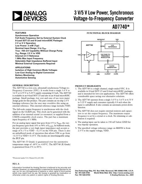
VIN<br />
FUNCTIONAL BLOCK DIAGRAM<br />
AD7740<br />
X1<br />
BUF<br />
REFIN/OUT<br />
GND<br />
VOLTAGE-TO-<br />
FREQUENCY<br />
MODULATOR<br />
CLKOUT<br />
VDD<br />
2.5V<br />
REFERENCE<br />
CLOCK<br />
GENERATION<br />
CLKIN<br />
FOUT<br />
PRODUCT HIGHLIGHTS<br />
1. The AD7740 is a single channel, single-ended VFC. It is<br />
available in 8-lead SOT-23 and 8-lead microSOIC packages,<br />
and is intended for low-cost applications. The AD7740 offers<br />
considerable space saving over alternative solutions.<br />
2. The AD7740 operates from a single 3.0 V <strong>to</strong> 3.6 V or 4.75 V<br />
<strong>to</strong> 5.25 V supply and consumes typically 0.9 mA when the<br />
input is unbuffered. It also contains an au<strong>to</strong>matic power-down<br />
function.<br />
3. The AD7740 does not require external resis<strong>to</strong>rs and capaci<strong>to</strong>rs<br />
<strong>to</strong> set the output frequency. The maximum output<br />
frequency is set by a crystal or a clock. No trimming or calibration<br />
is required.<br />
4. The analog input can be taken <strong>to</strong> 150 mV below GND for<br />
true bipolar operation.<br />
5. The specified voltage reference range on REFIN is from<br />
2.5 V <strong>to</strong> the supply voltage, VDD.<br />
One Technology Way, P.O. Box 9106, Norwood, MA 02062-9106, U.S.A.<br />
Tel: 781/329-4700 World Wide Web Site: http://www.analog.com<br />
Fax: 781/326-8703 © <strong>Analog</strong> <strong>Devices</strong>, Inc., 2001
AD7740 SPECIFICATIONS<br />
(VDD = 3.0 V <strong>to</strong> 3.6 V, 4.75 V <strong>to</strong> 5.25 V, GND = 0 V, REFIN = 2.5 V; CLKIN = 1 MHz; All<br />
specifications T MIN <strong>to</strong> T MAX unless otherwise noted.)<br />
K, Y Versions1 Parameter2 DC PERFORMANCE<br />
Integral Nonlinearity<br />
Min Typ Max Unit Test Conditions/Comments<br />
CLKIN = 32 kHz3 ± 0.012 % of Span4 Unbuffered Mode, External Clock at CLKIN<br />
CLKIN = 1 MHz ± 0.012 % of Span Unbuffered Mode, Crystal at CLKIN<br />
CLKIN = 32 kHz3 ± 0.018 % of Span Buffered Mode, External Clock at CLKIN<br />
CLKIN = 1 MHz ± 0.018 % of Span Buffered Mode, Crystal at CLKIN<br />
Offset Error ± 7 ± 35 mV Unbuffered Mode, VIN = 0 V<br />
± 7 ± 35 mV Buffered Mode, VIN = 0.1 V<br />
Gain Error ± 0.1 ± 0.7 % of Span<br />
Offset Error Drift3 ± 20 µV/°C<br />
Gain Error Drift3 ± 4 ppm of Span/°C<br />
<strong>Power</strong> Supply Rejection Ratio3 –55 dB ∆VDD = ± 5% (5 V)<br />
ANALOG INPUT, VIN<br />
–65 dB ∆VDD = ± 10% (3.3 V)<br />
Nominal Input Span<br />
0.1<br />
0 – VREF VDD – 0.2<br />
V<br />
V<br />
± 150 mV Overrange Available<br />
Buffered Mode<br />
Input Current 8 10 µA Unbuffered Mode, VIN = 5.4 V, REFIN = 5.25 V<br />
REFERENCE VOLTAGE<br />
REFIN<br />
5 100 nA Buffered Mode, VIN = 0.1 V, REFIN = 2.5 V<br />
5<br />
Nominal Input <strong>Voltage</strong><br />
REFOUT<br />
2.5 VDD V<br />
Output <strong>Voltage</strong> 2.3 2.5 2.7 V<br />
Output Impedance3 1 kΩSee Pin Function Description<br />
Reference Drift3 ± 50 ppm/°C<br />
Line Rejection3 –75 dB ∆VDD = ± 5% (5 V)<br />
Line Rejection3 –60 dB ∆VDD = ± 10% (3.3 V)<br />
Reference Noise (0.1 Hz <strong>to</strong> 10 Hz) 3 FOUT OUTPUT<br />
100 µV p–p<br />
Nominal Frequency Span<br />
LOGIC INPUTS (CLKIN, BUF)<br />
0.1 fCLKIN <strong>to</strong> 0.9 fCLKIN Hz VIN = 0 V <strong>to</strong> VREF. See Figure 2<br />
3<br />
CLKIN<br />
Input Frequency 32 1000 kHz For Specified Performance<br />
Input High <strong>Voltage</strong>, VIH 3.5 V VDD = 5 V ± 5%<br />
Input High <strong>Voltage</strong>, VIH 2.5 V VDD = 3.3 V ± 10%<br />
Input <strong>Low</strong> <strong>Voltage</strong>, VIL 0.8 V VDD = 5 V ± 5%<br />
Input <strong>Low</strong> <strong>Voltage</strong>, VIL 0.4 V VDD = 3.3 V ± 10%<br />
Input Current<br />
Pin Capacitance<br />
BUF<br />
3<br />
± 2<br />
10<br />
µA<br />
pF<br />
VIN = 0 V <strong>to</strong> VDD Input High <strong>Voltage</strong>, VIH 2.4 V VDD = 5 V ± 5%<br />
Input High <strong>Voltage</strong>, VIH 2.1 V VDD = 3.3 V ± 10%<br />
Input <strong>Low</strong> <strong>Voltage</strong>, VIL 0.8 V VDD = 5 V ± 5%<br />
Input <strong>Low</strong> <strong>Voltage</strong>, VIL 0.4 V VDD = 3.3 V ± 10%<br />
Input Current ± 100 nA<br />
Pin Capacitance<br />
LOGIC OUTPUTS (FOUT, CLKOUT)<br />
3 10 pF<br />
3<br />
Output High <strong>Voltage</strong>, VOH 4.0 V Output Sourcing 200 µA6 . VDD = 5 V ± 5%<br />
Output High <strong>Voltage</strong>, VOH 2.1 V Output Sourcing 200 µA6 . VDD = 3.3 V ± 10%<br />
Output <strong>Low</strong> <strong>Voltage</strong>, VOL 0.1 0.4 V Output Sinking 1.6 mA6 POWER REQUIREMENTS<br />
V DD 7 3.0 5.25 V<br />
I DD (Normal Mode) 8 0.9 1.25 mA V IH = VDD, V IL= GND. Unbuffered Mode<br />
I DD (Normal Mode) 8 1.1 1.5 mA V IH = VDD, V IL= GND. Buffered Mode<br />
I DD (<strong>Power</strong>-Down) 30 100 µA<br />
<strong>Power</strong>-Up Time 3 30 µs Exiting <strong>Power</strong>-Down (Ext. Clock at CLKIN)<br />
NOTES<br />
1Temperature range: K Version, 0°C <strong>to</strong> +85°C; Y Version, –40°C <strong>to</strong> +105°C; typical specifications are at 25°C.<br />
2See Terminology.<br />
3Guaranteed by design and characterization, not production tested.<br />
4Span = Max output frequency–Min output frequency.<br />
5Because this pin is bidirectional, any external reference must be capable of sinking/sourcing 400 µA in order <strong>to</strong> overdrive the internal reference.<br />
6These logic levels apply <strong>to</strong> CLKOUT only when it is loaded with one CMOS load.<br />
7Operation at VDD = 2.7 V is also possible with degraded specifications.<br />
8Outputs unloaded. IDD increases by CL × VOUT × fFOUT when FOUT is loaded. If using a crystal/resona<strong>to</strong>r as the clock source, IDD will vary depending on the crystal/resona<strong>to</strong>r<br />
type (see Clock Generation section).<br />
Specifications subject <strong>to</strong> change without notice.<br />
–2–<br />
REV. A
TIMING CHARACTERISTICS<br />
REV. A –3–<br />
(VDD = 3.0 V <strong>to</strong> 3.6 V, 4.75 V <strong>to</strong> 5.25 V, GND = O V, REFIN = 2.5 V)<br />
AD7740<br />
Parameter<br />
Limit at TMIN, TMAX<br />
VDD = 3.0 V <strong>to</strong> 3.6 V<br />
Limit at TMIN, TMAX<br />
VDD = 4.75 V <strong>to</strong> 5.25 V Unit Conditions/Comments<br />
fCLKIN 32 32 kHz min Clock Frequency<br />
1 1 MHz max<br />
tHIGH:tLOW 40:60 40:60 min Clock Mark/Space Ratio<br />
60:40 60:40 max<br />
t1 50 35 ns typ CLKIN Edge <strong>to</strong> FOUT Edge Delay<br />
t2 2.3 1.8 ns typ FOUT Rise Time<br />
t3 1.6 1.4 ns typ FOUT Fall Time<br />
t4 tHIGH ± 20 tHIGH ± 8 ns typ FOUT Pulsewidth<br />
NOTES<br />
1 Guaranteed by design and characterization, not production tested.<br />
2 All input signals are specified with tr = tf = 5 ns (10% <strong>to</strong> 90% of VDD) and timed from a voltage level of (V IL + V IH)/2.<br />
3See Figure 1.<br />
Specifications subject <strong>to</strong> change without notice.<br />
CLKIN<br />
FOUT<br />
ABSOLUTE MAXIMUM RATINGS*<br />
(T A = 25°C unless otherwise noted)<br />
t 1<br />
t 4<br />
1, 2, 3<br />
t HIGH<br />
t LOW<br />
VDD <strong>to</strong> GND . . . . . . . . . . . . . . . . . . . . . . . . . –0.3 V <strong>to</strong> +7 V<br />
<strong>Analog</strong> Input <strong>Voltage</strong> <strong>to</strong> GND . . . . . . . . –0.3 V <strong>to</strong> VDD + 0.3 V<br />
Reference Input <strong>Voltage</strong> <strong>to</strong> GND . . . . . –0.3 V <strong>to</strong> V DD + 0.3 V<br />
Logic Input <strong>Voltage</strong> <strong>to</strong> GND . . . . . . . . –0.3 V <strong>to</strong> VDD + 0.3 V<br />
FOUT <strong>Voltage</strong> <strong>to</strong> GND . . . . . . . . . . . –0.3 V <strong>to</strong> VDD + 0.3 V<br />
Operating Temperature Range<br />
Commercial (K Version) . . . . . . . . . . . . . . . . 0°C <strong>to</strong> +85°C<br />
Au<strong>to</strong>motive (Y Version) . . . . . . . . . . . . . . –40°C <strong>to</strong> +105°C<br />
S<strong>to</strong>rage Temperature Range . . . . . . . . . . . . –65°C <strong>to</strong> +150°C<br />
Junction Temperature (TJ Max) . . . . . . . . . . . . . . . . . . 150°C<br />
SOT-23 Package<br />
<strong>Power</strong> Dissipation . . . . . . . . . . . . . . . . . . (T J Max – T A)/θ JA<br />
θJA Thermal Impedance . . . . . . . . . . . . . . . . . . . . . 240°C/W<br />
Lead Temperature (10 secs) . . . . . . . . . . . . . . . . . . 300°C<br />
Reflow Soldering<br />
Peak Temperature . . . . . . . . . . . . . . . . . . . . 220 + 5/0°C<br />
Time at Peak Temperature . . . . . . . . . . . . 10 sec <strong>to</strong> 40 sec<br />
Figure 1. Timing Diagram<br />
CAUTION<br />
ESD (electrostatic discharge) sensitive device. Electrostatic charges as high as 4000 V readily<br />
accumulate on the human body and test equipment and can discharge without detection. Although<br />
the AD7740 features proprietary ESD protection circuitry, permanent damage may occur on<br />
devices subjected <strong>to</strong> high-energy electrostatic discharges. Therefore, proper ESD precautions are<br />
recommended <strong>to</strong> avoid performance degradation or loss of functionality.<br />
t 2<br />
t 3<br />
microSOIC Package<br />
<strong>Power</strong> Dissipation . . . . . . . . . . . . . . . . . (TJ Max – TA)/θJA<br />
θJA Thermal Impedance . . . . . . . . . . . . . . . . . . . . . 206°C/W<br />
θJC Thermal Impedance . . . . . . . . . . . . . . . . . . . . . . 44°C/W<br />
Lead Temperature (10 secs) . . . . . . . . . . . . . . . . . . . 300°C<br />
Reflow Soldering<br />
Peak Temperature . . . . . . . . . . . . . . . . . . . . . . 220 +5/0°C<br />
Time at Peak Temperature . . . . . . . . . . . . . 10 sec <strong>to</strong> 40 sec<br />
*Stresses above those listed under Absolute Maximum Ratings may cause permanent<br />
damage <strong>to</strong> the device. This is a stress rating only; functional operation of the<br />
device at these or any other conditions above those listed in the operational<br />
sections of this specification is not implied. Exposure <strong>to</strong> absolute maximum rating<br />
conditions for extended periods may affect device reliability.<br />
WARNING!<br />
ESD SENSITIVE DEVICE
AD7740<br />
8-LEAD microSOIC PIN NUMBERS*<br />
8-Lead microSOIC<br />
CLKOUT 1<br />
8 BUF<br />
CLKIN 2 AD7740<br />
microSOIC<br />
7 FOUT<br />
GND 3 TOP VIEW 6 VDD<br />
REFIN/OUT 4<br />
(Not <strong>to</strong> Scale)<br />
5 VIN<br />
PIN FUNCTION DESCRIPTIONS<br />
Pin<br />
No. Mnemonic Function<br />
1 CLKOUT The crystal/resona<strong>to</strong>r is tied between this pin and CLKIN. In the case of an external clock driving CLKIN, an<br />
inverted clock signal appears on this pin and can be used <strong>to</strong> drive other circuitry provided it is buffered first.<br />
2 CLKIN The master clock for the device may be in the form of a crystal/resona<strong>to</strong>r tied between this pin and CLKOUT.<br />
An external CMOS-compatible clock may also be applied <strong>to</strong> this input as the clock for the device. If CLKIN<br />
is inactive low for 1 ms (typ), the AD7740 au<strong>to</strong>matically enters power-down.<br />
3 GND Ground reference for all the circuitry on-chip.<br />
4 REFIN/OUT <strong>Voltage</strong> Reference Input. This is the reference input <strong>to</strong> the core of the VFC and defines the span of the VFC.<br />
If this pin is left unconnected, the internal 2.5 V reference is the default reference. Alternatively, a precision<br />
external reference may be used <strong>to</strong> overdrive the internal reference. The internal reference has high output<br />
impedance in order <strong>to</strong> allow it <strong>to</strong> be overdriven.<br />
5 VIN The analog input <strong>to</strong> the VFC. It has a nominal input range from 0 V <strong>to</strong> VREF which corresponds <strong>to</strong> an output<br />
frequency of 10% fCLKIN <strong>to</strong> 90% fCLKIN. It has a ±150 mV overrange. If buffered, it draws virtually no current<br />
from whatever source is driving it.<br />
6 VDD <strong>Power</strong> Supply Input. These parts can be operated at 3.3 V ± 10% or 5 V ± 5%. The supply should be<br />
adequately decoupled with a 10 µF and a 0.1 µF capaci<strong>to</strong>r <strong>to</strong> GND.<br />
7 FOUT Frequency Output. FOUT goes from 10% <strong>to</strong> 90% of fCLKIN, depending on VIN.<br />
8 BUF Buffered Mode Select Pin. When BUF is tied low, the VIN input is unbuffered and the range on the VIN<br />
pin is –0.15 V <strong>to</strong> VDD + 0.15 V. When it is tied high, VIN is buffered and the range on the VIN pin<br />
is restricted <strong>to</strong> 0.1 V <strong>to</strong> VDD – 0.2 V.<br />
*Note that the SOT-23 and microSOIC packages have different pinouts.<br />
PIN CONFIGURATIONS<br />
ORDERING GUIDE<br />
Package Branding<br />
Model Temperature Range Package Description Option Information<br />
AD7740KRM 0°C <strong>to</strong> 85°C microSOIC Package RM-8 VOK<br />
AD7740YRT –40°C <strong>to</strong> +105°C SOT-23 Package RT-8 VOY<br />
AD7740YRM –40°C <strong>to</strong> +105°C microSOIC Package RM-8 VOY<br />
–4–<br />
8-Lead SOT-23<br />
BUF 1<br />
8 CLKOUT<br />
FOUT 2 AD7740<br />
SOT-23<br />
7 CLKIN<br />
VDD 3 TOP VIEW 6 GND<br />
VIN 4<br />
(Not <strong>to</strong> Scale)<br />
5 REFIN/OUT<br />
REV. A
TERMINOLOGY<br />
INTEGRAL NONLINEARITY<br />
For the VFC, Integral Nonlinearity (INL) is a measure of the maximum<br />
deviation from a straight line passing through the actual<br />
endpoints of the VFC transfer function. The error is expressed in<br />
% of the actual frequency span:<br />
Frequency Span = FOUT(max) – FOUT(min)<br />
OFFSET ERROR<br />
Ideally, the output frequency for 0 V input voltage is 10% of<br />
f CLKIN in unbuffered mode. The deviation from this value referred<br />
<strong>to</strong> the input is the offset error at BUF = 0. In buffered mode the<br />
minimum output frequency (corresponding <strong>to</strong> 0.10 V minimum<br />
input voltage) is 13.2% of f CLKIN at V REF = 2.5 V. The deviation<br />
from this value referred <strong>to</strong> the input is the offset error at BUF = 1.<br />
Offset error is expressed in mV.<br />
GAIN ERROR<br />
This is a measure of the span error of the VFC. The gain is the<br />
scale fac<strong>to</strong>r that relates the input VIN <strong>to</strong> the output FOUT.<br />
The gain error is the deviation in slope of the actual VFC transfer<br />
characteristic from the ideal expressed as a percentage of the fullscale<br />
span. See Figure 2.<br />
OFFSET ERROR DRIFT<br />
This is a measure of the change in Offset Error with changes in<br />
temperature. It is expressed in µV/°C.<br />
GAIN ERROR DRIFT<br />
This is a measure of the change in Gain Error with changes in<br />
temperature. It is expressed in (ppm of span)/°C.<br />
REV. A –5–<br />
AD7740<br />
POWER SUPPLY REJECTION RATIO (PSRR)<br />
This indicates how the apparent input voltage of the VFC is<br />
affected by changes in the supply voltage. The input voltage is<br />
kept constant at 2 V, V REF is 2.5 V and the VDD supply is varied<br />
10% at 3.3 V and ±5% at 5 V. The ratio of the apparent change<br />
in input voltage <strong>to</strong> the change in VDD is measured in dBs.<br />
OUTPUT<br />
FREQUENCY<br />
FOUT<br />
0.9 fCLKIN 0.1<br />
f CLKIN<br />
0 OFFSET<br />
REFIN<br />
ERROR<br />
Figure 2. Offset and Gain<br />
GAIN ERROR<br />
IDEAL<br />
WITH OFFSET<br />
ERROR ONLY<br />
WITH OFFSET<br />
ERROR AND<br />
GAIN ERROR<br />
INPUT<br />
VOLTAGE<br />
VIN
AD7740–Typical Performance Characteristics<br />
INL ERROR – % of Span<br />
0.015<br />
0.01<br />
0.005<br />
0<br />
–0.005<br />
–0.01<br />
BUFFER OFF<br />
VDD = 5V<br />
REFIN = 2.5V<br />
CLKIN = 1MHz<br />
T A = 25C<br />
BUFFER ON<br />
–0.015<br />
–0.5 0 0.5 1<br />
VIN – V<br />
1.5 2 2.5<br />
TPC 1. INL vs. VIN (Buffered and<br />
Unbuffered)<br />
OFFSET ERROR – mV<br />
12<br />
8<br />
4<br />
0<br />
–4<br />
REFIN = 2.5V<br />
CLKIN = 1MHz<br />
TA = 25C<br />
BUF = 0<br />
GAIN ERROR<br />
GAIN ERROR<br />
OFFSET ERROR<br />
0.08<br />
0.04<br />
–8<br />
0 3 4<br />
VDD – V<br />
5<br />
–0.12<br />
6<br />
TPC 4. Offset and Gain Error vs. VDD<br />
REFOUT – V<br />
2.520<br />
2.515<br />
2.510<br />
2.505<br />
T A = 25C<br />
2.500<br />
2.5 3.0 3.5 4.0<br />
VDD – V<br />
4.5 5.0 5.5<br />
TPC 7. REFOUT vs. VDD<br />
0<br />
–0.04<br />
–0.08<br />
OFFSET ERROR – mV<br />
–60<br />
GAIN ERROR – % Span<br />
PSRR – dB<br />
–4<br />
–5<br />
–6<br />
–7<br />
V DD = 5V<br />
REFIN = 2.5V<br />
T A = 25C<br />
BUFFER ON<br />
BUFFER OFF<br />
–8<br />
0 200 400 600 800 1000<br />
–50<br />
–70<br />
CLKIN FREQUENCY – kHz<br />
TPC 2. Offset Error vs. CLKIN<br />
(Buffered and Unbuffered)<br />
VDD = 5V<br />
REFIN = 4.75V<br />
CLKIN = 1MHz<br />
T A = 25C<br />
BUFFER ON<br />
–80<br />
–1 0 1 2<br />
VIN – V<br />
3 4 5<br />
–6–<br />
BUFFER OFF<br />
TPC 5. PSRR vs. VIN (Buffered and<br />
Unbuffered)<br />
FOUT<br />
1<br />
CLKIN<br />
2<br />
CH1 2.00V CH2 2.00V M 2.00s<br />
TPC 8. Typical FOUT Pulse Train<br />
(VIN = VREF/4)<br />
GAIN ERROR – % Span<br />
I DD – mA<br />
0.1<br />
0.05<br />
0<br />
–0.05<br />
VDD = 5V<br />
REFIN = 5V<br />
T A = 25C<br />
CLKIN 1 MHz<br />
BUFFER<br />
OFF<br />
BUFFER ON<br />
VDD = 5V<br />
REFIN = 2.5V<br />
TA = 25C<br />
–0.1<br />
0 200 400 600 800 1000<br />
CLKIN FREQUENCY – kHz<br />
1.25<br />
1<br />
0.75<br />
0.5<br />
0.25<br />
TPC 3. Gain Error vs. CLKIN<br />
(Buffered and Unbuffered)<br />
BUFFER ON<br />
BUFFER OFF<br />
VDD = 5V<br />
REFIN = 5V<br />
T A = 25C<br />
C FOUT = 43pF<br />
C CLKOUT = 22pF<br />
0<br />
0 200 400 600 800 1000<br />
CLKIN FREQUENCY – kHz<br />
TPC 6. I DD vs. CLKIN (Buffered and<br />
Unbuffered)<br />
REV. A
GENERAL DESCRIPTION<br />
The AD7740 is a CMOS synchronous <strong>Voltage</strong>-<strong>to</strong>-Frequency<br />
Converter (VFC) which uses a charge-balance conversion<br />
technique. The input voltage signal is applied <strong>to</strong> a proprietary<br />
front-end based around an analog modula<strong>to</strong>r which converts the<br />
input voltage in<strong>to</strong> an output pulse train.<br />
The part also contains an on-chip 2.5 V bandgap reference and<br />
operates from a single 3.3 V or 5 V supply. A block diagram of<br />
the AD7740 is shown in Figure 3.<br />
VIN<br />
BUF<br />
GND<br />
SWITCHED<br />
CAPS<br />
SWITCHED<br />
CAPS<br />
INTEGRATOR<br />
COMPARATOR<br />
AD7740<br />
FOUT<br />
Figure 3. Block Diagram<br />
Input Amplifier Buffering and <strong>Voltage</strong> Range<br />
The analog input VIN can be buffered by setting BUF = 1. This<br />
presents a high impedance, typically 100 MΩ, which allows<br />
significant external source impedances <strong>to</strong> be <strong>to</strong>lerated. The VIN<br />
voltage range is now 0.1 V <strong>to</strong> VDD – 0.2 V. By setting BUF = 0<br />
the AD7740 input circuit accepts an analog input below GND<br />
and the analog input VIN has a voltage range from –0.15 V <strong>to</strong><br />
VDD + 0.15 V. In this case the input impedance is typically<br />
650 kΩ.<br />
The transfer function for the AD7740 is represented by:<br />
FOUT = 0.1 fCLKIN + 0.8 (VIN/VREF) fCLKIN<br />
It is shown in Figure 4 for unbuffered mode.<br />
FOUT MAX<br />
0.90 f CLKIN<br />
0.10 f CLKIN<br />
FOUT MIN<br />
–0.15V 0<br />
OUTPUT<br />
FREQUENCY<br />
FOUT<br />
AD7740<br />
VREF VREF + 0.15V<br />
Figure 4. Transfer Function<br />
Sample Calculation:<br />
VREF = 2.5 V, BUF = 0<br />
FOUT (min) = 0.1 fCLKIN + 0.8(–0.15/2.5) fCLKIN = 0.052 fCLKIN<br />
FOUT (max) = 0.1 fCLKIN + 0.8(2.65/2.5) fCLKIN<br />
= 0.948 fCLKIN<br />
INPUT<br />
VOLTAGE<br />
VIN<br />
REV. A –7–<br />
AD7740<br />
VFC Modula<strong>to</strong>r<br />
The analog input signal <strong>to</strong> the AD7740 is continuously sampled<br />
by a switched capaci<strong>to</strong>r modula<strong>to</strong>r whose sampling rate is set<br />
by a master clock. The input signal may be buffered on-chip<br />
(BUF = 1) before being applied <strong>to</strong> the sampling capaci<strong>to</strong>r of the<br />
modula<strong>to</strong>r. This isolates the sampling capaci<strong>to</strong>r charging currents<br />
from the analog input pin.<br />
This system is a negative feedback loop that acts <strong>to</strong> keep the net<br />
charge on the integra<strong>to</strong>r capaci<strong>to</strong>r at zero, by balancing charge<br />
injected by the input voltage with charge injected by VREF. The<br />
output of the compara<strong>to</strong>r provides the digital input for the 1-bit<br />
DAC, so that the system functions as a negative feedback loop<br />
that acts <strong>to</strong> minimize the difference signal. See Figure 5.<br />
INPUT<br />
INTEGRATOR<br />
–V REF<br />
COMPARATOR<br />
+V REF<br />
CLK<br />
AD7740<br />
Figure 5. Modula<strong>to</strong>r Loop<br />
1-BIT<br />
BITSTREAM<br />
The digital data that represents the analog input voltage is contained<br />
in the duty cycle of the pulse train appearing at the output<br />
of the compara<strong>to</strong>r. The output is a pulse train whose frequency<br />
depends on the analog input signal. A full-scale input gives an<br />
output frequency of 0.9 f CLKIN and zero-scale input gives an<br />
output frequency of 0.1 fCLKIN. The output allows simple interfacing<br />
<strong>to</strong> either standard logic families or op<strong>to</strong>-couplers. The<br />
pulsewidth of FOUT is fixed and is determined by the high period<br />
of CLKIN. The pulse is synchronized <strong>to</strong> the rising edge of the<br />
clock signal. The delay time between the edge of CLKIN and the<br />
edge of FOUT is typically 35 ns. Figure 6 shows the waveform<br />
of this frequency output. (See TPC 8.)<br />
f CLKIN<br />
FOUT = f CLKIN /2<br />
VIN = V REF /2<br />
FOUT = f CLKIN /5<br />
VIN = V REF /8<br />
FOUT = f CLKIN 3/10<br />
VIN = V REF /4<br />
3tCLKIN 4tCLKIN AVERAGE FOUT IS fCLKIN 3/10 BUT THE ACTUAL PULSE STREAM VARIES<br />
BETWEEN fCLKIN /3 and fCLKIN /4<br />
Figure 6. Frequency Output Waveforms<br />
If there is a step change in input voltage, there is a settling time<br />
that must elapse before valid data is obtained. This is typically<br />
two CLKIN cycles.
AD7740<br />
Clock Generation<br />
As distinct from the asynchronous VFCs that rely on the<br />
stability of an external capaci<strong>to</strong>r <strong>to</strong> set their full-scale frequency,<br />
the AD7740 uses an external clock <strong>to</strong> define the full-scale output<br />
frequency. The result is a more stable transfer function, which<br />
allows the designer <strong>to</strong> determine the system stability and drift<br />
based upon the selected external clock.<br />
The AD7740 requires a master clock input, which may be an<br />
external CMOS-compatible clock signal applied <strong>to</strong> the CLKIN<br />
pin (CLKOUT not used). For a frequency of 1 MHz, a crystal<br />
or resona<strong>to</strong>r can be connected between CLKIN and CLKOUT<br />
so that the clock circuit functions as a crystal controlled oscilla<strong>to</strong>r.<br />
Figure 7 shows a simple model of this.<br />
5M<br />
CLKIN CLKOUT<br />
C1 C2<br />
ON-CHIP<br />
CIRCUITRY<br />
OFF-CHIP<br />
CIRCUITRY<br />
Figure 7. On-Chip Oscilla<strong>to</strong>r<br />
Using the part with a crystal or ceramic resona<strong>to</strong>r between the<br />
CLKIN and CLKOUT pins generally causes more current <strong>to</strong><br />
be drawn from VDD than when the part is clocked from a driven<br />
clock signal at the CLKIN pin. This is because the on-chip<br />
oscilla<strong>to</strong>r is active in the case of the crystal or resona<strong>to</strong>r. The<br />
amount of additional current depends on a number of fac<strong>to</strong>rs.<br />
First, the larger the value of the capaci<strong>to</strong>r on CLKIN and<br />
CLKOUT pins, the larger the current consumption. Typical<br />
values recommended by the crystal and resona<strong>to</strong>r manufacturers<br />
are in the range of 30 pF <strong>to</strong> 50 pF. Another fac<strong>to</strong>r that influences<br />
IDD is Effective Series Resistance of the crystal (ESR).<br />
The lower the ESR value, the lower the current taken by the<br />
oscilla<strong>to</strong>r circuit.<br />
The on-chip oscilla<strong>to</strong>r also has a start-up time associated with it<br />
before it oscillates at its correct frequency and voltage levels. The<br />
typical start-up time is 10 ms with a VDD of 5 V and 15 ms with<br />
a VDD of 3.3 V (both with a 1 MHz crystal).<br />
The AD7740 master clock appears inverted on the CLKOUT<br />
pin of the device. The maximum recommended load on this pin is<br />
one CMOS load. When using a crystal <strong>to</strong> generate the AD7740’s<br />
clock it may be desirable <strong>to</strong> then use this clock as the clock<br />
source for the entire system. In this case, it is recommended that<br />
the CLKOUT signal be buffered with a CMOS buffer before<br />
being applied <strong>to</strong> the rest of the circuit (as shown in Figure 7).<br />
–8–<br />
Reference Input<br />
The AD7740 performs conversions relative <strong>to</strong> the applied reference<br />
voltage. This reference may be taken from the internal 2.5 V<br />
bandgap reference by leaving REFIN/OUT unconnected. Alternatively<br />
an external precision reference may be used. This is<br />
connected <strong>to</strong> the REFIN/OUT pin, overdriving the internal<br />
reference. Drive capability, initial error, noise, and drift characteristics<br />
should be considered when selecting an external reference.<br />
The AD780 and REF192 are suitable choices for external<br />
references.<br />
The internal reference is most suited <strong>to</strong> applications where<br />
ratiometric operation of the signal source is possible. Using the<br />
internal reference in systems where the signal source varies with<br />
time, temperature, loading, etc., tends <strong>to</strong> cancel out errors.<br />
<strong>Power</strong>-Down Mode<br />
When CLKIN is inactive low for 1 ms (typ), the AD7740 au<strong>to</strong>matically<br />
enters a power-down mode. In this mode most of the<br />
digital and analog circuitry is shut down and REFOUT floats.<br />
FOUT goes high. This reduces the power consumption <strong>to</strong> 525 µW<br />
max (5 V) and 360 µW (3.3 V).<br />
APPLICATIONS<br />
The basic connection diagram for the part is shown in Figure 8.<br />
In the connection diagram shown, the AD7740 is configured in<br />
unbuffered mode. The 5 V power supply is used as a reference <strong>to</strong><br />
the AD7740. A quartz crystal provides the master clock source<br />
for the part. It may be necessary <strong>to</strong> connect capaci<strong>to</strong>rs (C1 and<br />
C2 in the diagram) <strong>to</strong> the crystal <strong>to</strong> ensure that it does not oscillate<br />
at over<strong>to</strong>nes of its fundamental operating frequency. The<br />
values of capaci<strong>to</strong>rs will vary depending on the manufacturer’s<br />
specifications.<br />
VIN<br />
5V<br />
VDD<br />
AD7740<br />
REFIN<br />
FOUT<br />
GND<br />
BUF<br />
CLKIN CLKOUT<br />
C1 C2<br />
0.1F 10F<br />
Figure 8. Basic Connection Diagram<br />
REV. A
A/D Conversion Techniques Using the AD7740<br />
One method of using a VFC in an A/D system is <strong>to</strong> count the<br />
output pulses of FOUT for a fixed gate interval (see Figure 9).<br />
This fixed gate interval should be generated by dividing down<br />
the clock input frequency. This ensures that any errors due <strong>to</strong><br />
clock jitter or clock frequency drift are eliminated. The ratio of<br />
the FOUT frequency <strong>to</strong> the clock frequency is what is important<br />
here, not the absolute value of FOUT. The frequency division<br />
can be done by a binary counter where CLKIN is the<br />
counter input.<br />
VIN<br />
AD7740<br />
CLKIN<br />
CLOCK<br />
GENERATOR<br />
FOUT<br />
FREQUENCY<br />
DIVIDER<br />
COUNTER<br />
GATE<br />
SIGNAL<br />
TO P<br />
Figure 9. A/D Conversion Using the AD7740 VFC<br />
Figure 10 shows the waveforms of CLKIN, FOUT, and the<br />
Gate signal. A counter counts the rising edges of FOUT while the<br />
Gate signal is high. Since the gate interval is not synchronized with<br />
FOUT, there is a possibility of a counting inaccuracy. Depending<br />
on FOUT, an error of one count may occur.<br />
CLKIN<br />
FOUT<br />
GATE t GATE<br />
Figure 10. Waveforms in an A/D Converter Using a VFC<br />
The clock frequency and the gate time determine the resolution<br />
of such an ADC. If 12-bit resolution is required and CLKIN is<br />
1 MHz (therefore, FOUTMAX is 0.9 MHz), the minimum gate<br />
time required is calculated as follows:<br />
N counts at Full Scale (0.9 MHz) will take<br />
(N/0.9 × 106 ) seconds = minimum gate time<br />
N is the <strong>to</strong>tal number of codes for a given resolution; 4096 for<br />
12 bits.<br />
minimum gate time = (4096/0.9 × 106 ) seconds = 4.551 ms<br />
REV. A –9–<br />
AD7740<br />
Since TGATE × FOUTMAX = number of counts at full scale, the<br />
fastest conversion for a given resolution can be performed with<br />
the highest CLKIN frequency.<br />
If the output frequency is measured by counting pulses gated <strong>to</strong><br />
a signal derived from the clock, the clock stability is unimportant<br />
and the device simply performs as a voltage-controlled frequency<br />
divider, producing a high-resolution ADC. The inherent mono<strong>to</strong>nicity<br />
of the transfer function and wide range of input clock<br />
frequencies allows the conversion time and resolution <strong>to</strong> be<br />
optimized for specific applications.<br />
Another parameter is taken in<strong>to</strong> account when choosing the<br />
length of the gate interval. Because the integration period of the<br />
VFC is equal <strong>to</strong> the gate interval, any interfering signal can be<br />
rejected by counting for an integer number of periods of the<br />
interfering signal. For example, a gate interval of 100 ms will<br />
give normal-mode rejection of 50 Hz and 60 Hz signals.<br />
Isolation Applications<br />
The AD7740 can also be used in isolated analog signal transmission<br />
applications. Due <strong>to</strong> noise, safety requirements or distance,<br />
it may be necessary <strong>to</strong> isolate the AD7740 from any controlling<br />
circuitry. This can easily be achieved by using op<strong>to</strong>-isola<strong>to</strong>rs.<br />
This is extremely useful in overcoming ground loops between<br />
equipment.<br />
The analog voltage <strong>to</strong> be transmitted is converted <strong>to</strong> a pulse<br />
train using the VFC. An op<strong>to</strong>-isola<strong>to</strong>r circuit is used <strong>to</strong> couple<br />
this pulse train across an isolation barrier using light as the<br />
connecting medium. The input LED of the isola<strong>to</strong>r is driven<br />
from the output of the AD7740. At the receiver side, the output<br />
transis<strong>to</strong>r is operated in the pho<strong>to</strong>-transis<strong>to</strong>r mode. The pulse<br />
train can be reconverted <strong>to</strong> an analog voltage using a frequency<strong>to</strong>-voltage<br />
converter; alternatively, the pulse train can be fed in<strong>to</strong><br />
a counter <strong>to</strong> generate a digital signal.<br />
The analog and digital sections of the AD7740 have been designed<br />
<strong>to</strong> allow operation from a single-ended power source, simplifying<br />
its use with isolated power supplies.<br />
Figure 11 shows a general purpose VFC circuit using a low cost<br />
op<strong>to</strong>-isola<strong>to</strong>r. A 5 V power supply is assumed for both the isolated<br />
(VDD) and local (VCC) supplies.<br />
VIN<br />
V DD<br />
AD7740<br />
GND1<br />
0.1F 10F<br />
FOUT<br />
R<br />
ISOLATION<br />
BARRIER<br />
V CC<br />
OPTOCOUPLER<br />
GND2<br />
Figure 11. Op<strong>to</strong>-Isolated Application
AD7740<br />
Temperature Sensor Application<br />
The AD7740 can be used with an AD22100S temperature<br />
sensor <strong>to</strong> give a digital measure of ambient temperature. The<br />
output voltage of the AD22100S is proportional <strong>to</strong> the temperature<br />
times the supply voltage. It uses a single 5 V supply, and its<br />
output swings from 0.25 V at –50°C <strong>to</strong> 4.75 V at +150°C. By<br />
feeding its output through the AD7740, the value of ambient<br />
temperature is converted in<strong>to</strong> a digital pulse train. See Figure 12.<br />
V+<br />
AD22100S<br />
0.1F 10F 0.1F<br />
VIN<br />
5V<br />
VDD<br />
AD7740<br />
REFIN<br />
FOUT<br />
BUF<br />
GND<br />
CLKIN CLKOUT<br />
C1 C2<br />
10F<br />
Figure 12. Using the AD7740 with a Temperature Sensor<br />
Due <strong>to</strong> its ratiometric nature this application provides an<br />
extremely cost-effective solution. The need for an external precision<br />
reference is eliminated since the 5 V power-supply is used<br />
as a reference <strong>to</strong> both the VFC and the AD22100S.<br />
32 kHz Operation<br />
The AD7740 oscilla<strong>to</strong>r circuit will not operate at 32 kHz. If<br />
the user wishes <strong>to</strong> use a 32 kHz watch crystal, some additional<br />
external circuitry is required. The circuit in Figure 13 is for a<br />
crystal with a required drive of 1 µW. Resis<strong>to</strong>rs R1 and R2<br />
reduce the power <strong>to</strong> this level.<br />
32kHz<br />
R3<br />
1M<br />
40106 40106<br />
R2<br />
100k<br />
R1<br />
220k<br />
CLKIN<br />
Figure 13. 32 kHz Watch Crystal Circuit<br />
–10–<br />
<strong>Power</strong> Supply Bypassing and Grounding<br />
In any circuit where accuracy is important, careful consideration<br />
of the power supply and ground return layout helps <strong>to</strong> ensure<br />
the rated performance. The printed circuit board housing the<br />
AD7740 should be designed such that the analog and digital<br />
sections are separated and confined <strong>to</strong> certain areas of the board.<br />
To minimize capacitive coupling between them, digital and<br />
analog ground planes should only be joined in one place, close<br />
<strong>to</strong> the AD7740, and should not overlap.<br />
Avoid running digital lines under the device, as these will couple<br />
noise on<strong>to</strong> the die. The analog ground plane should be allowed<br />
<strong>to</strong> run under the AD7740 <strong>to</strong> avoid noise coupling. The power<br />
supply lines <strong>to</strong> the AD7740 should use as large a trace as possible<br />
<strong>to</strong> provide low impedance paths and reduce the effects of<br />
glitches on the power supply line. Fast switching signals like<br />
clocks should be shielded with digital ground <strong>to</strong> avoid radiating<br />
noise <strong>to</strong> other parts of the board, and clock signals should never<br />
be run near analog inputs. Avoid crossover of digital and analog<br />
signals. Traces on opposite sides of the board should run at right<br />
angles <strong>to</strong> each other. This reduces the effect of feedthrough<br />
through the board. A microstrip technique is by far the best but<br />
is not always possible with a double-sided board. In this technique,<br />
the component side of the board is dedicated <strong>to</strong> the ground plane<br />
while the signal traces are placed on the solder side.<br />
Good decoupling is also important. All analog supplies should<br />
be decoupled <strong>to</strong> GND with surface mount capaci<strong>to</strong>rs, 10 µF in<br />
parallel with 0.1 µF located as close <strong>to</strong> the package as possible,<br />
ideally right up against the device. The lead lengths on the bypass<br />
capaci<strong>to</strong>r should be as short as possible. It is essential that<br />
these capaci<strong>to</strong>rs be placed physically close <strong>to</strong> the AD7740 <strong>to</strong><br />
minimize the inductance of the PCB trace between the capaci<strong>to</strong>r<br />
and the supply pin. The 10 µF are the tantalum bead type and<br />
are located in the vicinity of the VFC <strong>to</strong> reduce low-frequency<br />
ripple. The 0.1 µF capaci<strong>to</strong>rs should have low Effective Series<br />
Resistance (ESR) and Effective Series Inductance (ESI), such<br />
as the common ceramic types, which provide a low impedance<br />
path <strong>to</strong> ground at high frequencies <strong>to</strong> handle transient<br />
currents due <strong>to</strong> internal logic switching. Additionally, it is beneficial<br />
<strong>to</strong> have large capaci<strong>to</strong>rs (> 47 µF) located at the point<br />
where the power connects <strong>to</strong> the PCB.<br />
REV. A
0.122 (3.10)<br />
0.114 (2.90)<br />
0.006 (0.15)<br />
0.002 (0.05)<br />
0.071 (1.80)<br />
0.059 (1.50)<br />
PIN 1<br />
0.051 (1.30)<br />
0.035 (0.90)<br />
OUTLINE DIMENSIONS<br />
Dimensions shown in inches and (mm).<br />
0.122 (3.10)<br />
0.114 (2.90)<br />
8 5<br />
8-Lead microSOIC<br />
(RM-8)<br />
REV. A –11–<br />
1<br />
PIN 1<br />
0.0256 (0.65) BSC<br />
SEATING<br />
PLANE<br />
0.006 (0.15)<br />
0.000 (0.00)<br />
4<br />
0.120 (3.05)<br />
0.112 (2.84)<br />
0.018 (0.46)<br />
0.008 (0.20)<br />
0.122 (3.10)<br />
0.110 (2.80)<br />
8 7 6 5<br />
1 2 3 4<br />
0.077 (1.95)<br />
BSC<br />
0.199 (5.05)<br />
0.187 (4.75)<br />
0.043 (1.09)<br />
0.037 (0.94)<br />
0.011 (0.28)<br />
0.003 (0.08)<br />
8-Lead SOT-23<br />
(RT-8)<br />
0.015 (0.38)<br />
0.009 (0.22)<br />
0.026 (0.65) BSC<br />
0.057 (1.45)<br />
0.035 (0.90)<br />
SEATING<br />
PLANE<br />
0.120 (3.05)<br />
0.112 (2.84)<br />
33<br />
27<br />
0.009 (0.23)<br />
0.003 (0.08)<br />
0.028 (0.71)<br />
0.016 (0.41)<br />
10<br />
0<br />
0.022 (0.55)<br />
0.014 (0.35)<br />
AD7740<br />
C01030a–2.5–2/01 (rev. A)<br />
PRINTED IN U.S.A.


