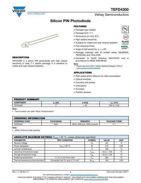
TEFD4300 Silicon PIN Photodiode - datasheets
TEFD4300 Silicon PIN Photodiode - datasheets
TEFD4300 Silicon PIN Photodiode - datasheets

Create successful ePaper yourself
Turn your PDF publications into a flip-book with our unique Google optimized e-Paper software.
DESCRIPTION<br />
www.vishay.com<br />
<strong>TEFD4300</strong> is a silicon <strong>PIN</strong> photodiode with high radiant<br />
sensitivity in clear, T-1 plastic package. It is sensitive to<br />
visible and near infrared radiation.<br />
PRODUCT SUMMARY<br />
Note<br />
• Test condition see table “Basic Characteristics”<br />
Note<br />
• MOQ: minimum order quantity<br />
<strong>Silicon</strong> <strong>PIN</strong> <strong>Photodiode</strong><br />
<strong>TEFD4300</strong><br />
Vishay Semiconductors<br />
FEATURES<br />
• Package type: leaded<br />
• Package form: T-1<br />
• Dimensions (in mm): Ø 3<br />
• High radiant sensitivity<br />
• Suitable for visible and near infrared radiation<br />
• Fast response times<br />
• Angle of half sensitivity: ϕ = ± 20°<br />
• Package matched with IR emitter series VSLB3940,<br />
TSUS4300, and TSAL4400<br />
• Compliant to RoHS Directive 2002/95/EC and in<br />
accordance to WEEE 2002/96/EC<br />
Note<br />
** Please see document “Vishay Material Category Policy”:<br />
www.vishay.com/doc?99902<br />
APPLICATIONS<br />
• High speed photo detector for data transmission<br />
• Optical switches<br />
• Counters and sorters<br />
• Interrupters<br />
•Encoders<br />
• Position sensors<br />
COMPONENT Ira (μA) ϕ (deg) λ0.1 (nm)<br />
<strong>TEFD4300</strong> 17 ± 20 350 to 1120<br />
ORDERING INFORMATION<br />
ORDERING CODE PACKAGING REMARKS PACKAGE FORM<br />
<strong>TEFD4300</strong> Bulk MOQ: 5000 pcs, 5000 pcs/bulk T-1<br />
ABSOLUTE MAXIMUM RATINGS (Tamb = 25 °C, unless otherwise specified)<br />
PARAMETER TEST CONDITION SYMBOL VALUE UNIT<br />
Reverse voltage VR 60 V<br />
Power dissipation Tamb ≤ 25 °C PV 215 mW<br />
Junction temperature Tj 100 °C<br />
Operating temperature range Tamb - 40 to + 100 °C<br />
Storage temperature range Tstg - 40 to + 100 °C<br />
Soldering temperature t ≤ 3 s, 2 mm from case Tsd 260 °C<br />
Thermal resistance junction/ambient Connected with Cu wire, 0.14 mm2 RthJA 450 K/W<br />
Rev. 1.1, 29-Nov-11 1<br />
For technical questions, contact: detectortechsupport@vishay.com<br />
Document Number: 83471<br />
THIS DOCUMENT IS SUBJECT TO CHANGE WITHOUT NOTICE. THE PRODUCTS DESCRIBED HEREIN AND THIS DOCUMENT<br />
ARE SUBJECT TO SPECIFIC DISCLAIMERS, SET FORTH AT www.vishay.com/doc?91000
www.vishay.com<br />
BASIC CHARACTERISTICS (Tamb = 25 °C, unless otherwise specified)<br />
BASIC CHARACTERISTICS (Tamb = 25 °C, unless otherwise specified)<br />
<strong>TEFD4300</strong><br />
Vishay Semiconductors<br />
PARAMETER TEST CONDITION SYMBOL MIN. TYP. MAX. UNIT<br />
Forward voltage IF = 50 mA VF 1 V<br />
Breakdown voltage IR = 100 μA, E = 0 V(BR) 60 V<br />
Reverse dark current VR = 10 V, E = 0 Iro 0.15 3 nA<br />
Diode capacitance<br />
VR = 0 V, f = 1 MHz, E = 0<br />
VR = 5 V, f = 1 MHz, E = 0<br />
CD<br />
CD<br />
3.3<br />
1.2<br />
pF<br />
pF<br />
Open circuit voltage Ee = 1 mW/cm2 , λ = 950 nm VOC 350 mV<br />
Temperature coefficient of VO Ee = 1 mW/cm2 , λ = 950 nm TKVo - 2.6 mV/K<br />
Short circuit current Ee = 1 mW/cm2 , λ = 950 nm Ik 15 μA<br />
Temperature coefficient of Ik Ee = 1 mW/cm2 , λ = 950 nm TKIk 0.1 %/K<br />
Reverse light current Ee = 1 mW/cm2 , λ = 950 nm, VR = 5 V Ira 9 17 27 μA<br />
Angle of half sensitivity ϕ ± 20 deg<br />
Wavelength of peak sensitivity λp 950 nm<br />
Range of spectral bandwidth λ0.1 350 1120 nm<br />
Rise time VR = 10 V, RL = 1 kΩ, λ = 820 nm tr 100 ns<br />
Fall time VR = 10 V, RL = 1 kΩ, λ = 820 nm tf 100 ns<br />
I r0 - Reverse Dark Current (A)<br />
10 -6<br />
10 -7<br />
10 -8<br />
10 -9<br />
10 -10<br />
10 -11<br />
10 -12<br />
V R = 10 V<br />
0 20 40 60 80 100<br />
T amb - Ambient Temperature (°C)<br />
0.6<br />
0 20<br />
40 60 80 100<br />
Fig. 1 - Reverse Dark Current vs. Ambient Temperature Fig. 2 - Relative Reverse Light Current vs. Ambient Temperature<br />
Rev. 1.1, 29-Nov-11 2<br />
For technical questions, contact: detectortechsupport@vishay.com<br />
Document Number: 83471<br />
THIS DOCUMENT IS SUBJECT TO CHANGE WITHOUT NOTICE. THE PRODUCTS DESCRIBED HEREIN AND THIS DOCUMENT<br />
ARE SUBJECT TO SPECIFIC DISCLAIMERS, SET FORTH AT www.vishay.com/doc?91000<br />
I ra, rel - Relative Reverse Light Current<br />
94 8416<br />
1.4<br />
1.2<br />
1.0<br />
0.8<br />
V R = 5 V<br />
λ = 950 nm<br />
T amb - Ambient Temperature (°C)
I ra - Reverse Light Current (μA)<br />
C p - Capacitance (pF)<br />
S(λ) rel - Relative Spectral Sensitivity<br />
100<br />
10<br />
1<br />
0.1<br />
0.01<br />
www.vishay.com<br />
t p = 100 μs, V R = 5 V, λ = 950 nm<br />
1 10 100 1000 10 000<br />
E e - Irradiance (μW/cm 2 )<br />
Fig. 3 - Reverse Light Current vs. Irradiance<br />
3.5<br />
3.0<br />
2.5<br />
2.0<br />
1.5<br />
1.0<br />
0.5<br />
f = 1 MHz, E = 0<br />
0<br />
0.01 0.1 1 10 100<br />
VR - Reverse Voltage (V)<br />
Fig. 4 - Diode Capacitance vs. Reverse Voltage<br />
1.0<br />
0.9<br />
0.8<br />
0.7<br />
0.6<br />
0.5<br />
0.4<br />
0.3<br />
0.2<br />
0.1<br />
0<br />
400 500 600 700 800 900 1000 1100<br />
λ - Wavelength (nm)<br />
Fig. 5 - Relative Spectral Sensitivity vs. Wavelength<br />
<strong>TEFD4300</strong><br />
Vishay Semiconductors<br />
0<br />
- 90 - 60 - 30 0 30 60 90<br />
ϕ - Angular Displacement (°)<br />
Fig. 6 - Relative Radiant Intensity vs. Angular Displacement<br />
Fig. 7 - Dark Current vs. Reverse Voltage<br />
Rev. 1.1, 29-Nov-11 3<br />
For technical questions, contact: detectortechsupport@vishay.com<br />
Document Number: 83471<br />
THIS DOCUMENT IS SUBJECT TO CHANGE WITHOUT NOTICE. THE PRODUCTS DESCRIBED HEREIN AND THIS DOCUMENT<br />
ARE SUBJECT TO SPECIFIC DISCLAIMERS, SET FORTH AT www.vishay.com/doc?91000<br />
S rel - Relative Sensitivity<br />
I r0 - Reverse Dark Current (A)<br />
1.0<br />
0.9<br />
0.8<br />
0.7<br />
0.6<br />
0.5<br />
0.4<br />
0.3<br />
0.2<br />
0.1<br />
10 -6<br />
10 -7<br />
10 -8<br />
10 -9<br />
10 -10<br />
10 -11<br />
10 -12<br />
100 °C<br />
75 °C<br />
50 °C<br />
25 °C<br />
0 °C<br />
0 5 10 15 20<br />
V R - Reverse Voltage (V)
www.vishay.com<br />
PACKAGE DIMENSIONS in millimeters<br />
30.6 ± 0.5<br />
6.1 ± 0.3<br />
4.5 ± 0.3<br />
0.6 ± 0.15<br />
2.54 nom.<br />
3.5 ± 0.1<br />
Drawing-No.: 6.544-5411.01-4<br />
Issue: 1; 25.05.11<br />
22618<br />
A<br />
3.2 ± 0.1<br />
C<br />
(2.5)<br />
3.9 ± 0.15<br />
< 0.6<br />
1.5 ± 0.25<br />
SENSITIVE AREA<br />
Ø 3 ± 0.1<br />
+ 0.15<br />
0.4 - 0.05<br />
<strong>TEFD4300</strong><br />
Vishay Semiconductors<br />
AREA NOT PLANE<br />
technical drawings<br />
according to DIN<br />
specifications<br />
Rev. 1.1, 29-Nov-11 4<br />
For technical questions, contact: detectortechsupport@vishay.com<br />
Document Number: 83471<br />
THIS DOCUMENT IS SUBJECT TO CHANGE WITHOUT NOTICE. THE PRODUCTS DESCRIBED HEREIN AND THIS DOCUMENT<br />
ARE SUBJECT TO SPECIFIC DISCLAIMERS, SET FORTH AT www.vishay.com/doc?91000
www.vishay.com<br />
Disclaimer<br />
Legal Disclaimer Notice<br />
Vishay<br />
ALL PRODUCT, PRODUCT SPECIFICATIONS AND DATA ARE SUBJECT TO CHANGE WITHOUT NOTICE TO IMPROVE<br />
RELIABILITY, FUNCTION OR DESIGN OR OTHERWISE.<br />
Vishay Intertechnology, Inc., its affiliates, agents, and employees, and all persons acting on its or their behalf (collectively,<br />
“Vishay”), disclaim any and all liability for any errors, inaccuracies or incompleteness contained in any datasheet or in any other<br />
disclosure relating to any product.<br />
Vishay makes no warranty, representation or guarantee regarding the suitability of the products for any particular purpose or<br />
the continuing production of any product. To the maximum extent permitted by applicable law, Vishay disclaims (i) any and all<br />
liability arising out of the application or use of any product, (ii) any and all liability, including without limitation special,<br />
consequential or incidental damages, and (iii) any and all implied warranties, including warranties of fitness for particular<br />
purpose, non-infringement and merchantability.<br />
Statements regarding the suitability of products for certain types of applications are based on Vishay’s knowledge of typical<br />
requirements that are often placed on Vishay products in generic applications. Such statements are not binding statements<br />
about the suitability of products for a particular application. It is the customer’s responsibility to validate that a particular<br />
product with the properties described in the product specification is suitable for use in a particular application. Parameters<br />
provided in <strong>datasheets</strong> and/or specifications may vary in different applications and performance may vary over time. All<br />
operating parameters, including typical parameters, must be validated for each customer application by the customer’s<br />
technical experts. Product specifications do not expand or otherwise modify Vishay’s terms and conditions of purchase,<br />
including but not limited to the warranty expressed therein.<br />
Except as expressly indicated in writing, Vishay products are not designed for use in medical, life-saving, or life-sustaining<br />
applications or for any other application in which the failure of the Vishay product could result in personal injury or death.<br />
Customers using or selling Vishay products not expressly indicated for use in such applications do so at their own risk. Please<br />
contact authorized Vishay personnel to obtain written terms and conditions regarding products designed for such applications.<br />
No license, express or implied, by estoppel or otherwise, to any intellectual property rights is granted by this document or by<br />
any conduct of Vishay. Product names and markings noted herein may be trademarks of their respective owners.<br />
Material Category Policy<br />
Vishay Intertechnology, Inc. hereby certifies that all its products that are identified as RoHS-Compliant fulfill the<br />
definitions and restrictions defined under Directive 2011/65/EU of The European Parliament and of the Council<br />
of June 8, 2011 on the restriction of the use of certain hazardous substances in electrical and electronic equipment<br />
(EEE) - recast, unless otherwise specified as non-compliant.<br />
Please note that some Vishay documentation may still make reference to RoHS Directive 2002/95/EC. We confirm that<br />
all the products identified as being compliant to Directive 2002/95/EC conform to Directive 2011/65/EU.<br />
Vishay Intertechnology, Inc. hereby certifies that all its products that are identified as Halogen-Free follow Halogen-Free<br />
requirements as per JEDEC JS709A standards. Please note that some Vishay documentation may still make reference<br />
to the IEC 61249-2-21 definition. We confirm that all the products identified as being compliant to IEC 61249-2-21<br />
conform to JEDEC JS709A standards.<br />
Revision: 02-Oct-12 1 Document Number: 91000