DIODE / THYRISTOR MODULE - Datasheets.pl
DIODE / THYRISTOR MODULE - Datasheets.pl
DIODE / THYRISTOR MODULE - Datasheets.pl

You also want an ePaper? Increase the reach of your titles
YUMPU automatically turns print PDFs into web optimized ePapers that Google loves.
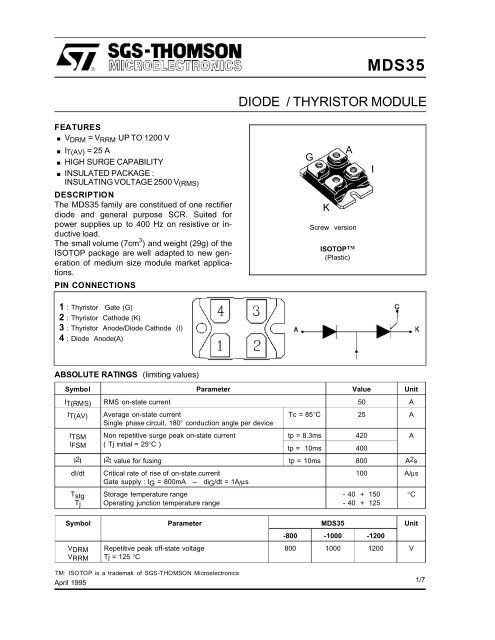
MDS35<strong>DIODE</strong> / <strong>THYRISTOR</strong> <strong>MODULE</strong>. V DRM =V RRM UP TO 1200 VFEATURES. I T(AV) =25A..HIGH SURGE CAPABILITYINSULATED PACKAGE :INSULATING VOLTAGE 2500 V (RMS)DESCRIPTIONThe MDS35 family are constitued of one rectifierdiode and general purpose SCR. Suited forpower sup<strong>pl</strong>ies up to 400 Hz on resistive or inductiveload.The small volume (7cm 3 ) and weight (29g) of theISOTOP package are well adapted to new generationof medium size module market ap<strong>pl</strong>ications.PIN CONNECTIONSGKAScrew versionISOTOP TM(Plastic)I1 : Thyristor Gate (G)2 : Thyristor Cathode (K)3 : Thyristor Anode/Diode Cathode (I)4 : Diode Anode(A)ABSOLUTE RATINGS (limiting values)Symbol Parameter Value UnitIT(RMS) RMS on-state current 50 AIT(AV) Average on-state currentSingle phase circuit, 180° conduction angle per deviceTc = 85°C 25 AITSM Non repetitive surge peak on-state currenttp = 8.3ms 420 AIFSM ( Tj initial = 25°C )tp = 10ms 400I2t I2t value for fusing tp = 10ms 800 A2sdI/dt Critical rate of rise of on-state current100 A/µsGate sup<strong>pl</strong>y : IG = 800mA – diG/dt = 1A/µsT stgTjStorage temperature rangeOperating junction temperature range- 40 + 150- 40 + 125°CSymbol Parameter MDS35 Unit-800 -1000 -1200VDRMVRRMRepetitive peak off-state voltageTj = 125 °C800 1000 1200 VTM: ISOTOP is a trademak of SGS-THOMSON MicroelectronicsApril 19951/7
MDS35THERMAL RESISTANCESSymbol Parameter Value UnitRth (j-c) DC Junction to case for DC 1 °C/WRth (c-h) Contact (case to heatsink) (4) 0.05 °C/W(4) With contact grease utilisationGATE CHARACTERISTICS (maximum values)PGM =50W(tp=20µs) PG (AV)= 1W IFGM = 4 A (tp = 20 µs) VRGM = 5V.ELECTRICAL CHARACTERISTICS (SCR)Symbol Test Conditions Value UnitIGT VD=12V (DC) RL=33Ω Tj=25°C MAX 50 mAVGT VD=12V (DC) RL=33Ω Tj=25°C MAX 1.5 VVGD VD=VDRM RL=3.3kΩ Tj=125°C MIN 0.2 Vtgt VD=VDRM IG = 500mAdI G /dt = 3A/µsTj=25°C TYP 2 µsI L I G =1.2 I GT Tj=25°C TYP 60 mAMAX 120I H I T = 0.5A gate open Tj=25°C TYP 40 mAMAX 80V TM I TM = 80A tp= 380µs Tj=25°C MAX 1.7 VI DRMIRRMV DRMVRRMRatedRatedTj=25°C MAX 0.05 mATj=125°C MAX 10tq I T = 80A V R =75V V D =67%V DRMdI/dt=30A/µs dV/dt=20V/µs Gate openTj=125°C TYP 100 µsdV/dt *Linear slope up to VD=67%VDRMgate openTj=125°C MIN 500 V/µs* For higher guaranteed values, <strong>pl</strong>ease consult us.ELECTRICAL CHARACTERISTICS (<strong>DIODE</strong>)Symbol Test Conditions Value UnitVF IF=80A Tj=25°C 1.7 VIR VR=VRRM Tj=125°C 10 mATj=25°C 50 µA2/7
Fig. 1 : Maximun Average Power dissipation versusaverage on-state current.(Sinusoidal waveform : Thyristor or Diode)MDS35Fig. 2 : Correlation between maximum average powerdissipation and maximum allowable temperature (Tamb)for different thermal resistances heatsink + contact.(Sinusoidal waveform : Thyristor or Diode)P(av)(W)P(av)(W)=180 o=30 o =60 o =90 o =180 o=120 oRth(c- a)=1.00oC/MRth(c-a)=1.25oC/WoRth(c-a)=0.75 C/WoRth(c-a)=O.50 C/WRth(c.a)=0oC/WIT,IF(av)(A)oTamb( C)Fig. 3 : Maximum average power dissipation versusaverage on-state current.(Rectangular waveform : Thyristor or Diode)Fig.4 : Correlation between maximum average powerdissipation and maximum allowable temperature (Tamb)for different thermal resistances heatsink + contact.(Rectangular waveform : Thyristor or Diode)P(av)(W)=60o =90 o =120o o=180o=30DCI T,IF(av)(A)Fig.5 : Maximum total power dissipation versus outputcurrent on resistive or inductive load.(Single phase bridge rectifier : 2 packages MDS35)Fig. 6 : Correlation between maximum total averagepower dissipation and maximum ambiant allowabletemperature for different thermal resistances heatsink +contact.(Single phase bridge rectifier : 2 packages : MDS35)Ptot.(W)160o=180RESISTIVELOADINDU CTIVELOAD14012010080oRth(c.a)=0 C/WRth(c-a)=O.25oC/WRth(c-a)=0.5 oC/WRth(c-a)=1.0oC/W60Ioutput(A)40 Rth(c-a)=O.75oC/W20Tamb( oC)00 10 30 50 70 90 110 1303/7
MDS35Fig. 7 : Maximun total power dissipation versus outputcurrent .(Three phase bridge rectifier : 3 packages : MDS35)Ptot.(W)300Fig.8 : Correlation between maximum average powerdissipation and maximum allowable temperature (Tamb)for different thermal resistances heatsink + contact .(Three phase bridge rectifier : 3 packages : MDS35)Ptot.(W)250200150100o=120Rth(c.a)=0 OC/WORth(c-a)=O.25 C/WRth(c-a)=0.5 OC/WORth(c-a)=1.0 C/WORth(c-a)=0.75 C/W50Ioutput(A)00 10 20 30 40 50 60 70 80Fig. 9 : Average on-state current versus casetemperature .(Sinusoidal waveform : Thyristor or Diode)I T,IF(av)(A)Fig. 10 : Average on-state current versus casetemperature .(Rectangular waveform : Thyristor or Diode)IT,IF(av)(A)Tamb( oC)=180 o=120 oD.C.=90 o=60 o=180o=120o=30 oTcase(oC)o=90=60oo=30oTcase( c)Fig. 11: Relative variation of thermal transientimpedance junction to case versus pulse duration.Fig.12 : Relative variation of gate trigger and holdingcurrent versus junction temperature.Igt;Ih [Tj] / Igt;Ih [Tj=25 C]oIgtIhtp(s)oTj( C)4/7
Fig.13 : Non repetitive surge peak on-state current for asinusoidal pulse with width : tp ≤ 10 ms andcorresponding value of I 2 t.(Thyristor or diode)I TSM;IFSM(A);I2t(A2s)oTj initial = 25 CITSM;IFSM(A)Tj initial = 25 o CMDS35Fig. 14 : Non repetitive surge peak on-state currentversus number of cycles.(Thyristor or Diode)2I tITSM;IFSMtp(ms)Number of cycles2 5Fig. 15 : On-state characteristics .(Maximum values)(Thyristor or Diode)VTM,VFM(V)Tj=125oC:Vto=0.85VRt=11mTj initial = 25 o CoTj initial = 125 CITM,IFM(A)5/7
MDS35PACKAGE MECHANICAL DATAISOTOP <strong>pl</strong>astic : SCREW VERSIONMAGOJ /OBOI /OI /HDEFCKLPscrew H M4REF.DIMENSIONSMillimeters InchesMin. Max. Min. Max.A 11.80 12.20 0.465 0.480B 8.90 9.10 0.350 0.358C 1.95 2.05 0.077 0.081D 0.75 0.85 0.029 0.034E 12.60 12.80 0.496 0.504F 25.10 25.50 0.988 1.004G 31.50 31.70 1.240 1.248H 4.00 0.157I 4.10 4.30 0.161 0.169J 4.10 4.30 0.161 0.169K 14.90 15.10 0.586 0.595L 30.10 30.30 1.185 1.193M 37.80 38.20 1.488 1.504O 7.80 8.20 0.307 0.323P 5.50 0.216Cooling method : CMarking : Type numberWeight : 28 g. (without screws)Electrical isolation : 2500V(RMS)Capacitance : < 45 pFInductance : < 5 nH- Recommended torque value : 1.3 N.m (Max 1.5 N.m) for the 6 x M4 screws. (2 x M4 screws recommended formounting the package on the heatsink and the 4 screws given with the screw version).- The screws sup<strong>pl</strong>ied with the package are adapted for mounting on a board (or others types of terminals) with athickness of 0.6 mm min and 2.2 mm max.6/7
MDS35Information furnished is believed to be accurate and reliable. However, SGS-THOMSON Microelectronics assumes no responsability forthe consequences of use of such information nor for any infringement of patents or other rights of third parties which may result from itsuse. No license is granted by im<strong>pl</strong>ication or otherwise under any patent or patent rights of SGS-THOMSON Microelectronics. Specificationsmentioned in this publication are subject to change without notice. This publication supersedes and re<strong>pl</strong>aces all information previouslysup<strong>pl</strong>ied.SGS-THOMSON Microelectronics products are not authorized for use as critical components in life support devices or systems withoutexpress written approval of SGS-THOMSON Microelectronics.© 1995 SGS-THOMSON Microelectronics - Printed in Italy - All rights reserved.SGS-THOMSON Microelectronics GROUP OF COMPANIESAustralia - Brazil - France - Germany - Hong Kong - Italy - Japan - Korea - Malaysia - Malta - Morocco - The Netherlands -Singapore - Spain - Sweden - Switzerland - Taiwan - Thailand - United Kingdom - U.S.A.7/7