


You also want an ePaper? Increase the reach of your titles
YUMPU automatically turns print PDFs into web optimized ePapers that Google loves.
Features<br />
2 channel integrated analog input Class D audio<br />
amplifier in a small 7 x 7 mm PQFN44 package<br />
No mechanical heatsink required<br />
High peak music power output<br />
Split or single power supply<br />
Differential or single-ended input<br />
Over-current, over-temperature and under<br />
voltage protections with self-reset feature<br />
Start/stop click noise reduction<br />
Clip and Fault reporting outputs<br />
High noise immunity<br />
RoHS compliant<br />
Typical Applications<br />
Home theatre systems<br />
Docking station audio systems<br />
PC audio systems<br />
Musical instruments<br />
Karaoke amplifiers<br />
Game consoles<br />
Powered speaker systems<br />
General purpose audio power amplifiers<br />
Typical Connection<br />
Product Summary<br />
<strong>IR43x2</strong><br />
Topology<br />
Half-Bridge,<br />
Full-Bridge<br />
IR4302 Output power<br />
130 W/ 4 Ω<br />
(Typical, THD+N=10%)<br />
100 W/ 3 Ω<br />
IR4322 Output power<br />
(Typical, THD+N=10%)<br />
IR4312 Output power<br />
(Typical, THD+N=10%)<br />
*Residual noise<br />
(AES-17, IHF-A, typical)<br />
*THD+N<br />
(1kHz, 1W, 4 Ω, typical)<br />
* In typical application example<br />
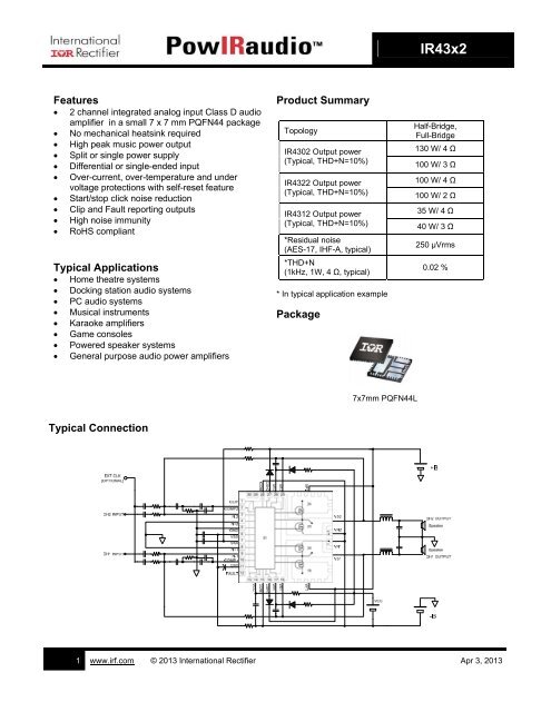
Package<br />
7x7mm PQFN44L<br />
100 W/ 4 Ω<br />
100 W/ 2 Ω<br />
35 W/ 4 Ω<br />
40 W/ 3 Ω<br />
250 μVrms<br />
0.02 %<br />
1 www.irf.com © 2013 <strong>International</strong> <strong>Rectifier</strong> Apr 3, 2013
<strong>IR43x2</strong><br />
Table of Contents Page<br />
Typical Connection Diagram 1<br />
Qualification Information 4<br />
Absolute Maximum Ratings 5<br />
Recommended Operating Conditions 7<br />
Electrical Characteristics 8<br />
Functional Block Diagram 11<br />
Input/Output Pin Equivalent Circuit Diagram 12<br />
Lead Definitions 14<br />
Lead Assignments 15<br />
Package Details 16<br />
Part Marking Information 17<br />
Ordering Information 17<br />
2 www.irf.com © 2013 <strong>International</strong> <strong>Rectifier</strong> Apr 3, 2013
Description<br />
<strong>IR43x2</strong><br />
The <strong>IR43x2</strong> integrates 2 channel PWM controller and digital audio MOSFETs forming a high performance Class D<br />
audio amplifier. As a result of fully optimized MOSFETs co-packed with a dedicated controller IC, the IR43X2<br />
operates without mechanical heatsink attached in a typical music playback usage. High voltage ratings and noise<br />
immunity in the controller IC ensures reliable operation over various environmental conditions. A small 7x7 mm<br />
PQFN package enhances the benefit of smaller size of Class D topology. The IR43X2 series is a lead-free, ROHS<br />
compliant.<br />
Typical Connection Diagram<br />
1. Inverting Amplifier<br />
2. Differential Amplifier<br />
3 www.irf.com © 2013 <strong>International</strong> <strong>Rectifier</strong> Apr 3, 2013
3. Single Power Supply (Inverting Amplifier)<br />
Qualification Information †<br />
Industrial ††<br />
<strong>IR43x2</strong><br />
Qualification Level<br />
Comments: This family of ICs has passed JEDEC’s Industrial<br />
qualification. IR’s Consumer qualification level is granted by<br />
extension of the higher Industrial level.<br />
Moisture Sensitivity Level<br />
MSL2<br />
(per IPC/JEDEC J-STD-020C)<br />
Machine Model<br />
Class A<br />
(per JEDEC standard EIA/JESD22-A115)<br />
IR4302M<br />
Class 1B<br />
ESD Human Body Model<br />
IR4322M<br />
IR4312M<br />
(per EIA/JEDEC standard JESD22-A114)<br />
Class 1A<br />
(per EIA/JEDEC standard JESD22-A114)<br />
IC Latch-Up Test<br />
Class I, Level A<br />
(per JESD78)<br />
RoHS Compliant Yes<br />
† Qualification standards can be found at <strong>International</strong> <strong>Rectifier</strong>’s web site http://www.irf.com/<br />
†† Higher qualification ratings may be available should the user have such requirements. Please contact your<br />
<strong>International</strong> <strong>Rectifier</strong> sales representative for further information.<br />
††† Higher MSL ratings may be available for the specific package types listed here. Please contact your <strong>International</strong><br />
<strong>Rectifier</strong> sales representative for further information.<br />
4 www.irf.com © 2013 <strong>International</strong> <strong>Rectifier</strong> Apr 3, 2013
<strong>IR43x2</strong><br />
Absolute Maximum Ratings<br />
Absolute Maximum Ratings indicate sustained limits beyond which damage to the device may occur. All voltage<br />
parameters are absolute voltages referenced to COM=VN1=VN2; all currents are defined positive into any lead.<br />
The Thermal Resistance and Power Dissipation ratings are measured under board mounted and still air<br />
conditions.<br />
Symbol Definition Min Max Units<br />
IR4302 - 80<br />
VPn Positive power supply rail voltage, n=1-2<br />
IR4322 - 60<br />
IR4312 - 40<br />
IR4302 -0.3 95<br />
VBn High side floating supply voltage<br />
IR4322 -0.3 75<br />
VSn High side floating supply voltage<br />
IR4312 -0.3 55<br />
†† , n=1-2 VBn -15 VBn +0.3<br />
VCSHn<br />
VCC<br />
CSH pin input voltage, n=1-2<br />
Low side supply voltage<br />
VSn -0.3 VBn +0.3<br />
†† -0.3 15<br />
IR4302 -0.3 100<br />
VAA Floating input positive supply voltage IR4322 -0.3 70<br />
††<br />
IR4312 -0.3 50<br />
VSS Floating input negative supply voltage ††<br />
V<br />
-1<br />
(See ISSZ)<br />
GND +0.3<br />
VIN+n Floating input supply ground voltage , n=1-2 VSS -0.3 VAA +0.3<br />
IINn Input current between IN- and IN+ pins † , n=1-2 - ±3 mA<br />
VCSD CSD pin input voltage VSS -0.3 VAA +0.3<br />
VCOMPn COMP pin input voltage, n=1-2 VSS -0.3 VAA +0.3 V<br />
VCLIP CLIP pin input voltage GND -0.3 VAA +0.3<br />
ICLIP CLIP pin sinking current - 5 mA<br />
VFAULT FAULT pin input voltage GND -0.3 VAA +0.3 V<br />
IFAULT FAULT pin sinking current - 5<br />
IAAZ Floating input supply zener clamp current †† - 20<br />
ISSZ Floating input negative supply zener clamp current †† - 20<br />
ICCZ Low side supply zener clamp current ††† - 20<br />
IBSZn Floating supply zener clamp current ††† mA<br />
, n=1-2 - 20<br />
dVSn/dt Allowable Vs voltage slew rate, n=1-2 - 50 V/ns<br />
dVSS/dt Allowable Vss voltage slew rate ††† - 50 V/ms<br />
Id@ 25ºC<br />
Id@ 100ºC<br />
IDM<br />
Continuous output current, from VPn to VSn, VSn<br />
to VNn, VCC=10V, VBn-VSn=10V<br />
Continuous output current, from VPn to VSn, VSn<br />
to VNn, VCC=10V, VBn-VSn=10V<br />
Pulsed output current, from VPn to VSn, VSn to<br />
VNn, VCC=10V, VBn-VSn=10V †††††<br />
IR4302 6.5<br />
IR4322 -<br />
7.0<br />
IR4312<br />
3.6<br />
IR4302 5.4<br />
IR4322 -<br />
5.8<br />
IR4312<br />
2.9<br />
IR4302 26<br />
IR4322 -<br />
28<br />
IR4312<br />
15<br />
5 www.irf.com © 2013 <strong>International</strong> <strong>Rectifier</strong> Apr 3, 2013<br />
A
<strong>IR43x2</strong><br />
IR4302 25<br />
Pd Power dissipation IR4322 25<br />
†††† @ TC = 25C<br />
-<br />
IR4312<br />
8<br />
RthJC Thermal resistance, junction to ambient<br />
IR4302<br />
IR4322<br />
5<br />
5<br />
††††<br />
IR4312<br />
-<br />
-<br />
14<br />
TJIC Control IC junction temperature - 150<br />
TJFET FET junction temperature - 150<br />
TS Storage Temperature -55 150<br />
TL Lead temperature (Soldering, 10 seconds) - 300<br />
† IN- and IN+ contain clamping diodes between the two pins.<br />
†† VAA -VSS, Vcc-COM and VBn-VSn contain internal shunt zener diodes. Note that the voltage<br />
ratings of these can be limited by the clamping current.<br />
††† For the rising and falling edges of step signal of 10V. Vss=15V to 200V.<br />
†††† Per MOSFET<br />
††††† Repetitive rating, pulse width limited by max. junction temperature<br />
6 www.irf.com © 2013 <strong>International</strong> <strong>Rectifier</strong> Apr 3, 2013<br />
W<br />
C/W<br />
C
<strong>IR43x2</strong><br />
Recommended Operating Conditions<br />
For proper operation, the device should be used within the recommended conditions below. The Vss and Vsn<br />
offset ratings are tested with supplies biased at COM=VN1=VN2, VAA-VSS=9.6V, VCC=12V and VBn-VSn=12V. All<br />
voltage parameters are absolute voltages referenced to COM; all currents are defined positive into any lead.<br />
Symbol Definition Min Max Units<br />
Positive power supply voltage, n=1-2, without<br />
heatsink<br />
IR4302<br />
IR4322<br />
-<br />
-<br />
46<br />
46<br />
VPn<br />
Positive power supply voltage, n=1-2, with<br />
heatsink<br />
IR4312<br />
IR4302<br />
IR4322<br />
-<br />
-<br />
-<br />
32<br />
62<br />
50<br />
IR4312 - 32<br />
VBn High side floating supply absolute voltage, n=1-2 VSn +10 VSn +14<br />
IR4302 † 80<br />
VSn High side floating supply offset voltage, n=1-2 IR4322 † 60<br />
IR4312 † 40<br />
VAA Floating input positive supply voltage †† VSS + 4.5 VSS + 15<br />
VSS<br />
Floating input negative supply voltage ††<br />
IR4302 0 80<br />
IR4322 0 60<br />
IR4312 0 40<br />
IAAZ Floating input supply zener clamp current †† 1 15<br />
ISSZ Floating input negative supply zener clamp current †† 1 15<br />
VCC Low side fixed supply voltage 10 15<br />
VIC IN- and IN+ pins common mode input voltage VSS + 2 VAA - 2<br />
VIN-n Inverting input voltage, n=1-2 VIN+ -0.5 VIN+ +0.5<br />
VCSD CSD pin input voltage VSS VAA<br />
VCOMPn COMP pin input voltage, n=1-2 VSS VAA<br />
CCOMPn COMP pin phase compensation capacitor to GND , n=1-2 1 - nF<br />
VCSHn CSH pin input voltage, n=1-2 VSn VBn V<br />
dVss/dt Allowable Vss voltage slew rate upon power-up ††† - 50 V/ms<br />
fSW Switching Frequency - 500 kHz<br />
TA Ambient Temperature -40 100 C<br />
†<br />
Logic operational for Vs equal to –5V to +80V. Logic state held for Vs equal to –5V to –VBS.<br />
††<br />
†††<br />
GND input voltage is limited by IAAZ and ISSZ.<br />
Vss ramps up from 0V to 70V.<br />
7 www.irf.com © 2013 <strong>International</strong> <strong>Rectifier</strong> Apr 3, 2013<br />
V<br />
mA<br />
V
<strong>IR43x2</strong><br />
Electrical Characteristics<br />
VCC,VBS= 12 V, VSS=VS1=VS2=VN1=VN2=COM=0V, VAA=9.6V and TA=25C unless otherwise specified.<br />
Symbol Definition<br />
Low Side Supply<br />
UVCC+<br />
Vcc supply UVLO positive<br />
threshold<br />
UVCC-<br />
Vcc supply UVLO negative<br />
threshold<br />
Min<br />
Typ<br />
8 www.irf.com © 2013 <strong>International</strong> <strong>Rectifier</strong> Apr 3, 2013<br />
Max<br />
Units<br />
8.4 8.9 9.4 V<br />
8.2 8.7 9.2 V<br />
Test Conditions<br />
UVCCHYS UVCC hysteresis - 0.2 - V<br />
IQCC Low side quiescent current - - 3 mA<br />
ICC Low side supply current - 10 - mA f=400kHz<br />
VCLAMPLn<br />
Low side zener diode clamp<br />
voltage, n=1-2<br />
14.7 15.3 16.2 V ICC=5mA<br />
High Side Floating Supply<br />
UVBS+n<br />
High side well UVLO<br />
positive threshold, n=1-2<br />
8.0 8.5 9.0 V<br />
UVBS-n<br />
High side well UVLO<br />
negative threshold, n=1-2<br />
7.8 8.3 8.8 V<br />
UVBSHYSn UVBS hysteresis, n=1-2 - 0.2 - V<br />
IQBSn<br />
High side quiescent current,<br />
n=1-2<br />
- - 2.4 mA<br />
VCLAMPHn<br />
High side zener diode clamp<br />
voltage, n=1-2<br />
14.7 15.3 16.2 V IBS=5mA<br />
Floating Input Supply<br />
UVAA+<br />
UVAA-<br />
VA+, VA- floating supply<br />
UVLO positive threshold<br />
from VSS<br />
VA+, VA- floating supply<br />
UVLO negative threshold<br />
from VSS<br />
8.2 8.7 9.2 V<br />
7.7 8.2 8.7 V<br />
UVAAHYS UVAA hysteresis - 0.5 - V<br />
IQAA0<br />
IQAA1<br />
IQAA2<br />
ILKM<br />
VCLAMPM+<br />
VCLAMPM-<br />
Floating Input positive<br />
quiescent supply current<br />
Floating Input positive<br />
quiescent supply current<br />
Floating Input positive<br />
quiescent supply current<br />
Floating input side to Low<br />
side leakage current<br />
VAA floating supply zener<br />
diode clamp voltage,<br />
positive, with respect to<br />
GND<br />
VSS floating supply zener diode<br />
clamp voltage, negative, with<br />
respect to GND<br />
- 1.5 3 mA<br />
- 4 6 mA<br />
- 5 7.5 mA<br />
- - 50 µA<br />
4.9 5.1 5.4 V<br />
-5.4 -5.1 -4.9 V<br />
VSS =0V, GND<br />
pin floating<br />
VSS =0V, GND<br />
pin floating<br />
VSS =0V, GND<br />
pin floating<br />
VAA=9.6V, VSS<br />
=0V,<br />
VCSD =VSS<br />
VAA=9.6V, VSS<br />
=0V,<br />
VCSD =VAA<br />
VAA=9.6V, VSS<br />
=0V,<br />
VCSD =GND<br />
VAA=VSS=VGND=<br />
100V<br />
IAA=5mA,<br />
ISS=5mA,<br />
VGND=0V,<br />
VCSD =VSS<br />
IAA=5mA,<br />
ISS=5mA,<br />
VGND=0V,<br />
VCSD =VSS
<strong>IR43x2</strong><br />
Electrical Characteristics (cont’d)<br />
VCC,VBS= 12 V, VSS=VS1=VS2=VN1=VN2=COM=0V, VAA=9.6V and TA=25C unless otherwise specified.<br />
Symbol Definition<br />
Min Typ Max Units Test Conditions<br />
Audio Input (VGND=0, VAA=4.8V, VSS=-4.8V)<br />
VOSn Input offset voltage, n=1-2 -18 0 18 mV<br />
IBINn Input bias current, n=1-2 - - 40 nA<br />
GBWn<br />
Small signal bandwidth in<br />
OTA, n=1-2<br />
- 9 - MHz<br />
CCOMP=1nF,<br />
Rf=0<br />
gmn OTA transconductance, n=1-2 - 10 - mS<br />
VIN+=0V, VIN-<br />
=10mV<br />
GVn<br />
PWM<br />
OTA gain, n=1-2 50 - - dB<br />
VthPWM<br />
PWM comparator threshold in<br />
COMP<br />
-<br />
(VAA -<br />
VSS)/2<br />
- V<br />
fOTAn<br />
COMP pin star-up local<br />
oscillation frequency, n=1-2<br />
0.7 1.0 1.5 MHz VCSD =GND<br />
Ton_n<br />
COMP to VS rising edge<br />
propagation delay, n=1-2<br />
- 370 - ns<br />
Toff_n<br />
COMP to VS trailing edge<br />
propagation delay, n=1-2<br />
- 320 - ns<br />
DTn<br />
Deadtime: Low-side turn-off to<br />
High-side turn-on (DTLO-HO) &<br />
High-side turn-off to Low-side<br />
turn-on (DTHO-LO) , n=1-2<br />
- 50 - ns<br />
VP=30V,<br />
VN=-30V,<br />
Power MOSFET (FET1, FET2, FET3, FET4) (IR4302)<br />
V(BR)DSS<br />
Drain-to-Source breakdown<br />
voltage<br />
80 - - V<br />
VGS=0V,<br />
ID=250uA<br />
RDS(ON) FET on resistance - 39 50 mΩ<br />
VGS=10V,<br />
ID=3.3A<br />
Qg Total gate charge - 7.3 - nC<br />
ILK0<br />
ILK1<br />
VP leakage current, VS=VN<br />
VP leakage current, VS=VP<br />
-<br />
-<br />
-<br />
-<br />
20<br />
50<br />
µA<br />
µA<br />
VP=80V, VCSD<br />
=VSS<br />
Power MOSFET (FET1, FET2, FET3, FET4) (IR4322)<br />
V(BR)DSS<br />
Drain-to-Source breakdown<br />
voltage<br />
60 - - V<br />
VGS=0V,<br />
ID=250uA<br />
RDS(ON) FET on resistance - 30 40 mΩ<br />
VGS=10V,<br />
ID=3.3A<br />
Qg Total gate charge - 8.3 - nC<br />
ILK0<br />
ILK1<br />
VP leakage current, VS=VN<br />
VP leakage current, VS=VP<br />
-<br />
-<br />
-<br />
-<br />
20<br />
50<br />
µA<br />
µA<br />
VP=60V, VCSD<br />
=VSS<br />
Power MOSFET (FET1, FET2, FET3, FET4) (IR4312)<br />
V(BR)DSS<br />
Drain-to-Source breakdown<br />
voltage<br />
40 - - V<br />
VGS=0V,<br />
ID=250uA<br />
RDS(ON) FET on resistance - 44 56 mΩ ID=3.6A<br />
Qg Total gate charge - 4.5 - nC VGS=10V<br />
ILK0 VP leakage current, VS=VN - - 20 µA<br />
VP=40V, VCSD<br />
=VSS<br />
ILK1 VP leakage current, VS=VP - - 50 µA<br />
9 www.irf.com © 2013 <strong>International</strong> <strong>Rectifier</strong> Apr 3, 2013
<strong>IR43x2</strong><br />
Electrical Characteristics (cont’d)<br />
VCC,VBS= 12 V, VSS=VS1=VS2=VN1=VN2=COM=0V, VAA=9.6V and TA=25C unless otherwise specified.<br />
Symbol Definition<br />
Min Typ Max Units<br />
Protection<br />
IOCPn<br />
Over current detection<br />
Positive threshold, n=1-2<br />
- 16 - A<br />
IOCNn<br />
Over current detection<br />
Negatitive threshold, n=1-2<br />
- -16 - A<br />
Vth1<br />
CSD pin shutdown release<br />
threshold<br />
0.62xVAA 0.70xVAA 0.78xVAA V<br />
Vth2 CSD pin self reset threshold 0.26xVAA 0.30xVAA 0.34xVAA V<br />
ICSD+ CSD pin discharge current 70 100 130 µA<br />
ICSD- CSD pin charge current 70 100 130 µA<br />
tSDn<br />
tOCPn<br />
tOCNn<br />
Vth+CLIP<br />
Vth-CLIP<br />
tCLIP<br />
tCLIPmin<br />
TSD<br />
TSDHYS<br />
Shutdown propagation delay<br />
from VS < Vth1 to Shutdown,<br />
n=1-2<br />
CHn propagation delay time<br />
from IOn > IOCPn to Shutdown,<br />
n=1-2<br />
CHn propagation delay time<br />
from IOn < IOCNn to Shutdown,<br />
n=1-2<br />
Clip detection positive<br />
threshold in COMP<br />
Clip detection negative<br />
threshold in COMP<br />
Clipping detection<br />
propagation delay<br />
Clipping detection minimum<br />
output duration<br />
Over temperature shutdown<br />
threshold in controller IC<br />
Over temperature shutdown<br />
threshold hysteresis<br />
Test Conditions<br />
VCSD = VSS<br />
+4.8V<br />
VCSD = VSS<br />
+4.8V<br />
- - 250 ns COMP = VSS<br />
- - 500 ns COMP = VSS<br />
- - 500 ns COMP = VSS<br />
0.85xVAA 0.90xVAA 0.95xVAA V<br />
0.05xVAA 0.10xVAA 0.15xVAA V<br />
- 40 - ns<br />
- 3 - us<br />
- 105 - ºC<br />
- 7 - ºC<br />
10 www.irf.com © 2013 <strong>International</strong> <strong>Rectifier</strong> Apr 3, 2013
Functional Bock Diagram<br />
<strong>IR43x2</strong><br />
11 www.irf.com © 2013 <strong>International</strong> <strong>Rectifier</strong> Apr 3, 2013
Input/Output Pin Equivalent Circuit Diagrams<br />
200 V<br />
<strong>IR43x2</strong><br />
12 www.irf.com © 2013 <strong>International</strong> <strong>Rectifier</strong> Apr 3, 2013<br />
10k<br />
15 V<br />
Clamp<br />
15 V<br />
Clamp<br />
V CC<br />
ESD<br />
Diode<br />
ESD<br />
Diode<br />
ESD<br />
Diode<br />
ESD<br />
Diode<br />
CSHn<br />
VBn<br />
HOn<br />
VSn<br />
VCC<br />
LOn<br />
COM<br />
COM2<br />
G<br />
G<br />
VPn<br />
D<br />
S<br />
D<br />
S<br />
VNn
Input/Output Pin Equivalent Circuit Diagrams (Cont’d)<br />
VAA<br />
CSD<br />
VSS<br />
ESD<br />
Diode<br />
ESD<br />
Diode<br />
CHARGE<br />
DISCHARGE<br />
<strong>IR43x2</strong><br />
13 www.irf.com © 2013 <strong>International</strong> <strong>Rectifier</strong> Apr 3, 2013
Lead Definitions<br />
Pin #<br />
Symbol Description<br />
<strong>IR43x2</strong><br />
1 CLIP Clipping detection output, open drain, referenced to GND<br />
2 COMP2 CH2 PWM comparator input<br />
3 IN-2 CH2 Analog inverting input<br />
4 IN+2 CH2 Analog non-inverting input<br />
5 GND GND for internal shunt zener diodes to VAA and VSS<br />
6 VSS Floating input negative supply<br />
7 VAA Floating input positive supply<br />
8 IN+1 CH1 Analog non-inverting input<br />
9 IN-1 CH1 Analog inverting input<br />
10 COMP1 CH1 PWM comparator input<br />
11 CSD Shutdown timing capacitor / shutdown input<br />
12 FAULT Fault reporting output, open drain, referenced to GND<br />
13 NC<br />
14 VCC Low side supply<br />
15 COM Low side supply return, internally connected to pin 31<br />
16 CSH1 CH1 High side over current sensing input, referenced to VS1<br />
17 VB1 CH1 High side floating supply<br />
18 VS1 CH1 PWM output, internally connected to pin 20<br />
19 VP1 CH1 Positive power supply<br />
20 VS1 CH1 PWM output<br />
21 VN1 CH1 Negative power supply, connect to COM externally<br />
22 VN2 CH2 Negative power supply, connect to COM externally<br />
23 VS2 CH2 PWM output, internally connected to pin 25<br />
24 VP2 CH2 Positive power supply<br />
25 VS2 CH2 PWM output<br />
26 VB2 CH2 High side floating supply<br />
27 CSH2 CH2 High side over current sensing input, referenced to VS2<br />
28 COM Low side supply return, internally connected to pin 31<br />
29 NC<br />
30 NC<br />
31 COM Low side supply return<br />
14 www.irf.com © 2013 <strong>International</strong> <strong>Rectifier</strong> Apr 3, 2013
Lead Assignments (Top View)<br />
<strong>IR43x2</strong><br />
15 www.irf.com © 2013 <strong>International</strong> <strong>Rectifier</strong> Apr 3, 2013
Package Details<br />
<strong>IR43x2</strong><br />
16 www.irf.com © 2013 <strong>International</strong> <strong>Rectifier</strong> Apr 3, 2013
<strong>IR43x2</strong><br />
Board Mounting Information<br />
Refer to Application Note AN-1170 Audio Power Quad Flat No-Lead (PQFN) Board Mounting Application Note.<br />
Part Marking Information<br />
Ordering Information<br />
Standard Pack<br />
Base Part Number Package Type<br />
Complete Part Number<br />
Form Quantity<br />
IR4302M<br />
PQFN44<br />
7x7mm Tape and Reel 3000 IR4302MTRPBF<br />
IR4322M<br />
PQFN44<br />
7x7mm Tape and Reel 3000 IR4322MTRPBF<br />
IR4312M<br />
PQFN44<br />
7x7mm Tape and Reel 3000 IR4312MTRPBF<br />
The information provided in this document is believed to be accurate and reliable. However, <strong>International</strong><br />
<strong>Rectifier</strong> assumes no responsibility for the consequences of the use of this information. <strong>International</strong><br />
<strong>Rectifier</strong> assumes no responsibility for any infringement of patents or of other rights of third parties which<br />
may result from the use of this information. No license is granted by implication or otherwise under any<br />
patent or patent rights of <strong>International</strong> <strong>Rectifier</strong>. The specifications mentioned in this document are<br />
subject to change without notice. This document supersedes and replaces all information previously<br />
supplied.<br />
For technical support, please contact IR’s Technical Assistance Center<br />
http://www.irf.com/technical-info/<br />
WORLD HEADQUARTERS:<br />
101 N. Sepulveda Blvd., El Segundo, California 90245<br />
Tel: (310) 252-7105<br />
17 www.irf.com © 2013 <strong>International</strong> <strong>Rectifier</strong> Apr 3, 2013


