

New Materials and Technologies Solve Hermetic SMD Integration
New Materials and Technologies Solve Hermetic SMD Integration
New Materials and Technologies Solve Hermetic SMD Integration

You also want an ePaper? Increase the reach of your titles
YUMPU automatically turns print PDFs into web optimized ePapers that Google loves.
<strong>New</strong> <strong>Materials</strong> <strong>and</strong> <strong>Technologies</strong> <strong>Solve</strong> <strong>Hermetic</strong> <strong>SMD</strong> <strong>Integration</strong><br />
by Tiva Bussarakons, International Rectifier, Inc., El Segundo, California<br />
as appeared in PCIM Power Electronic Systems Magazine, December 1999<br />
<strong>Hermetic</strong> semiconductor<br />
<strong>SMD</strong>s (surface-mount devices)<br />
can now be successfully <strong>and</strong> economically<br />
integrated in most system<br />
designs because of the:<br />
- Availability of low temperature<br />
coefficient of expansion<br />
(TCE) board materials<br />
-<br />
Advances in materials<br />
- Innovative <strong>SMD</strong> carrier designs<br />
- Maturity of power module<br />
technology<br />
Prior to these advancements,<br />
popularity of hermetic <strong>SMD</strong><br />
semiconductors was hindered by the TCE incompatibility<br />
between the package <strong>and</strong> board materials <strong>and</strong><br />
significantly wider operating temperature dem<strong>and</strong>s. The<br />
soldered interface of the assembly could crack when<br />
subjected to temperature extremes, i.e., after a soldering<br />
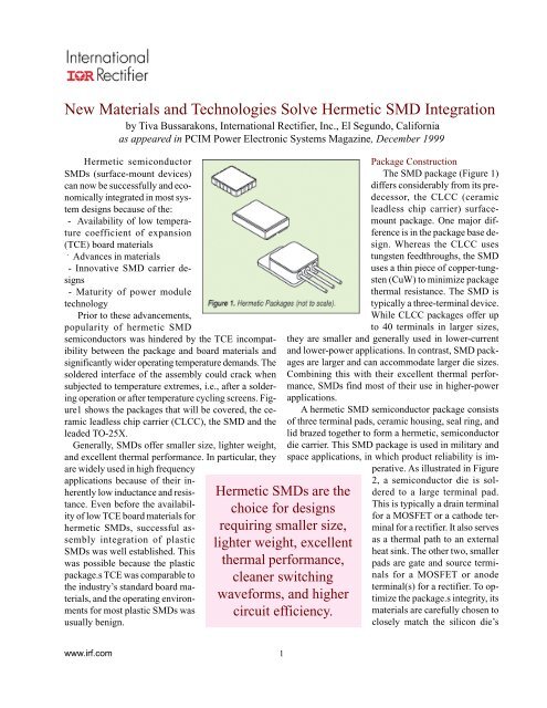
operation or after temperature cycling screens. Figure1<br />
shows the packages that will be covered, the ceramic<br />
leadless chip carrier (CLCC), the <strong>SMD</strong> <strong>and</strong> the<br />
leaded TO-25X.<br />
Generally, <strong>SMD</strong>s offer smaller size, lighter weight,<br />
<strong>and</strong> excellent thermal performance. In particular, they<br />
are widely used in high frequency<br />
applications because of their inherently<br />
low inductance <strong>and</strong> resistance.<br />
Even before the availability<br />
of low TCE board materials for<br />
hermetic <strong>SMD</strong>s, successful assembly<br />
integration of plastic<br />
<strong>SMD</strong>s was well established. This<br />
was possible because the plastic<br />
package.s TCE was comparable to<br />
the industry’s st<strong>and</strong>ard board materials,<br />
<strong>and</strong> the operating environments<br />
for most plastic <strong>SMD</strong>s was<br />
usually benign.<br />
<strong>Hermetic</strong> <strong>SMD</strong>s are the<br />
choice for designs<br />
requiring smaller size,<br />
lighter weight, excellent<br />
thermal performance,<br />
cleaner switching<br />
waveforms, <strong>and</strong> higher<br />
circuit efficiency.<br />
Package Construction<br />
The <strong>SMD</strong> package (Figure 1)<br />
differs considerably from its predecessor,<br />
the CLCC (ceramic<br />
leadless chip carrier) surfacemount<br />
package. One major difference<br />
is in the package base design.<br />
Whereas the CLCC uses<br />
tungsten feedthroughs, the <strong>SMD</strong><br />
uses a thin piece of copper-tungsten<br />
(CuW) to minimize package<br />
thermal resistance. The <strong>SMD</strong> is<br />
typically a three-terminal device.<br />
While CLCC packages offer up<br />
to 40 terminals in larger sizes,<br />
they are smaller <strong>and</strong> generally used in lower-current<br />
<strong>and</strong> lower-power applications. In contrast, <strong>SMD</strong> packages<br />
are larger <strong>and</strong> can accommodate larger die sizes.<br />
Combining this with their excellent thermal performance,<br />
<strong>SMD</strong>s find most of their use in higher-power<br />
applications.<br />
A hermetic <strong>SMD</strong> semiconductor package consists<br />
of three terminal pads, ceramic housing, seal ring, <strong>and</strong><br />
lid brazed together to form a hermetic, semiconductor<br />
die carrier. This <strong>SMD</strong> package is used in military <strong>and</strong><br />
space applications, in which product reliability is imperative.<br />
As illustrated in Figure<br />
2, a semiconductor die is soldered<br />
to a large terminal pad.<br />
This is typically a drain terminal<br />
for a MOSFET or a cathode terminal<br />
for a rectifier. It also serves<br />
as a thermal path to an external<br />
heat sink. The other two, smaller<br />
pads are gate <strong>and</strong> source terminals<br />
for a MOSFET or anode<br />
terminal(s) for a rectifier. To optimize<br />
the package.s integrity, its<br />
materials are carefully chosen to<br />
closely match the silicon die’s<br />
www.irf.com<br />
1
TCE, which is 4.2 ppm/°C. Table 1 lists<br />
the TCEs of these materials.<br />
Package Comparison<br />
Each <strong>SMD</strong> package is designed to<br />
accommodate a specific die size. Package<br />
piece parts are shaped to eliminate<br />
excess material without compromising<br />
mechanical integrity. This<br />
results in the smallest, lightest package<br />
possible. Terminal pads are solid<br />
CuW. The thin structure of the drain<br />
pad (in case of a FET) represents a<br />
very short thermal path from the heat<br />
source (die) to an external heat sink.<br />
Combined with the outst<strong>and</strong>ing thermal<br />
conductivity property of CuW, the<br />
package produces a very low thermal<br />
resistance path, thus a very low package<br />
junction-to-case thermal resistance<br />
(θ JC<br />
). Performance of various<br />
<strong>SMD</strong> <strong>and</strong> leaded (TO-254, TO-257<br />
<strong>and</strong> TO-258) devices are tabulated in<br />
Table 2.<br />
The following analyses are based<br />
on the same die size for each of the<br />
package comparisons. The die sizes<br />
are noted in Table 2. <strong>SMD</strong> 0.5 is the<br />
smallest <strong>SMD</strong> package in production<br />
today <strong>and</strong> is normally used in place of<br />
the TO-257. <strong>SMD</strong> 1 is about twice<br />
the size of the <strong>SMD</strong> 0.5 <strong>and</strong> is comparable<br />
to the TO-254. <strong>SMD</strong> 2 <strong>and</strong><br />
<strong>SMD</strong> 3 are the largest packages of the<br />
series <strong>and</strong> are usually used in place of<br />
the TO-258. In all instances, the<br />
<strong>SMD</strong> devices are superior to their<br />
leaded counterparts with respect to<br />
weight reduction <strong>and</strong> footprint<br />
requirements. The packages’ thermal<br />
resistances are comparable in all cases.<br />
When integrating <strong>SMD</strong> devices to<br />
an assembly, TCE of the board/substrate<br />
material must be closely<br />
matched to <strong>SMD</strong>’s TCE, typically<br />
within 2-3 ppm/°C to minimize<br />
mechanical stress <strong>and</strong> insure mechanical<br />
integrity. In addition, proper cooling<br />
must be provided to insure that<br />
the devices’ operating junction temperatures<br />
are maintained below the<br />
desired level under the worst case<br />
condition. A device’s thermal characteristics,<br />
θ JC<br />
<strong>and</strong> θ JA<br />
(junction-to-<br />
Figure 2. <strong>SMD</strong> package, cross-section view (not to scale).<br />
<strong>SMD</strong> Elements Material TCE ppm/°C<br />
Die Silicon 4.2<br />
Terminal Pads CuW 6.0<br />
Housing Al 2<br />
O 3<br />
6.4<br />
Seal Ring Kovar 5.1<br />
Lid Kovar 5.1<br />
Table 1. TCE property of <strong>SMD</strong> elements.<br />
ambient thermal resistance) are<br />
essential <strong>and</strong> must be considered in<br />
the design process.<br />
Low Power Designs<br />
<strong>SMD</strong> <strong>and</strong> CLCC devices can be<br />
attached directly to the traditional<br />
FR-4 or polyimide p.c. boards. However,<br />
due to considerable TCE mismatch,<br />
this assembly integration is<br />
limited to smaller packages. To circumvent<br />
solder joint fatigue, many<br />
designers empirically limit the package<br />
size to a maximum of 0.5 in. in any<br />
one dimension.<br />
For designs with larger <strong>SMD</strong> packages<br />
<strong>and</strong>/or with wide temperature<br />
extremes, low TCE board materials<br />
are the solution because of the availability<br />
of materials with a TCE of 7-9<br />
ppm/°C. Other TCE control techniques<br />
for p.c. boards include the use<br />
of molybdenum, copper-invar-copper,<br />
or para-aramid fiber reinforcement as<br />
the board stiffener.<br />
<strong>SMD</strong>s can be bonded to a board<br />
with a silver-filled epoxy or a soldering<br />
process. For an attachment using solder,<br />
eutectic alloys should be used.<br />
Preheating of the assembly prior to<br />
Package Typical Footprint θ JC<br />
Weight (gms) Required (in. 2 ) (°C/W)<br />
<strong>SMD</strong> .5 1.1 0.118 1.67 (1)<br />
TO-257 7.0 0.340 (4) 1.67 (1)<br />
<strong>SMD</strong> 1 2.6 0.281 0.83 (2)<br />
TO-254 9.3 0.521 (4) 0.83 (2)<br />
<strong>SMD</strong> 2 3.3 0.362 0.42 (3)<br />
<strong>SMD</strong> 3 3.4 0.387 0.42 (3)<br />
TO-258 10.9 0.693 (4) 0.42 (3)<br />
Notes:<br />
1) With size 3 die (0.116W x 0.181-in.L)<br />
2) With size 5 die (0.257W x 0.257-in.L)<br />
3) With size 6 die (0.260W x 0.360-in.L)<br />
4) Including lead length of 0.150-in.<br />
Table 2. Mechanical <strong>and</strong> thermal performance data of <strong>SMD</strong> <strong>and</strong> leaded packages.
Figure 3. <strong>SMD</strong> with Leads.<br />
soldering <strong>and</strong> allowing the assembly to<br />
cool naturally after a soldering process<br />
are highly recommended. Exposing<br />
<strong>SMD</strong> components to higher than<br />
300°C may cause permanent damage.<br />
Because FR-4 <strong>and</strong> polyimide board<br />
materials are poor thermal conductors,<br />
the p.c. board should not be considered<br />
as a thermal medium or heat<br />
spreader unless its copper traces are<br />
sufficiently large. Otherwise, cooling<br />
the semiconductor relies almost<br />
entirely on the package’s ability to<br />
dissipate thermal losses in the free<br />
convection environment. The package’s<br />
θ JA<br />
then becomes the key design<br />
parameter.<br />
For the aerospace environment<br />
where convection is nonexistent <strong>and</strong><br />
radiation cooling is minimal, conduction<br />
is the only meaningful cooling<br />
method. For cooling, it may be necessary<br />
to attach an <strong>SMD</strong> to an on-board<br />
heat spreader or an enlarged copper<br />
trace.<br />
For a device dissipating 1W with θ JA<br />
of 25°C/W, the junction temperature<br />
equals 100°C for an 75°C ambient.<br />
This is based on:<br />
(<br />
P = T J − T A )<br />
D<br />
θ<br />
JA<br />
(1)<br />
Where:<br />
P D<br />
= Device power dissipation<br />
T J<br />
= Operating junction temperature<br />
T A<br />
= Ambient temperature<br />
θ JA<br />
= Package junction-to-ambient<br />
thermal resistance<br />
High Power Designs<br />
For high-power applications where<br />
<strong>SMD</strong> devices dissipate more than a<br />
few watts <strong>and</strong> must be cooled with a<br />
heat sink, there are three basic assembly<br />
integration techniques. One<br />
Figure 4. St<strong>and</strong>ard <strong>SMD</strong> Carriers.<br />
approach is the <strong>SMD</strong> with leads<br />
assembly technique, where the <strong>SMD</strong><br />
is attached with flat copper leads for<br />
electrical connections. The <strong>SMD</strong><br />
semiconductor is bonded to a heat<br />
sink or a heat spreader via its lid, using<br />
a thermally conductive epoxy or a<br />
thermal pad for cooling. The <strong>SMD</strong><br />
semiconductor is electrically isolated<br />
from the heat sink because the lid is<br />
isolated from the die. The junctionto-lid<br />
thermal resistance for <strong>SMD</strong> 2 is<br />
about 6°C/W. Thermal resistance of<br />
the epoxy must be included when<br />
determining the total thermal resistance<br />
of the assembly. Figure 3 depicts<br />
a typical <strong>SMD</strong> with leads.<br />
Another common assembly technique<br />
is to bond the leaded surfaces of<br />
the <strong>SMD</strong> semiconductor directly to a<br />
heat sink with a thermally conductive<br />
epoxy or thermal pad. Unless the<br />
bonding medium contains an insulating<br />
material, placing a thin layer of<br />
ceramic at the bonding interface will<br />
provide the required electrical isolation.<br />
For assembly designs with one or<br />
two <strong>SMD</strong> devices, the <strong>SMD</strong> carrier is<br />
the solution to a cost-effective design.<br />
An <strong>SMD</strong> carrier is a leaded DBC<br />
(direct bond copper) substrate with<br />
three extended flat copper leads (one<br />
each for gate, drain, <strong>and</strong> source terminal<br />
as in the case of a MOSFET ).<br />
The <strong>SMD</strong> semiconductor is soldered<br />
to the carrier, providing an isolated<br />
ready-to-use <strong>SMD</strong> assembly. With its<br />
good thermal conductivity <strong>and</strong> excellent<br />
dielectric properties, the ceramic<br />
layer within the DBC provides the<br />
essential electrically isolated thermal<br />
path with negligible impact on the<br />
overall thermal performance of the<br />
assembly. St<strong>and</strong>ard <strong>SMD</strong> carriers are<br />
shown in Figure 4.<br />
Figure 5 illustrates a design implementation<br />
using <strong>SMD</strong> carrier assemblies.<br />
Here, all small-signal <strong>and</strong> lowpower<br />
components are populated on a<br />
FR-4 or polyimide board <strong>and</strong> each<br />
<strong>SMD</strong> is attached to a carrier. The<br />
<strong>SMD</strong> carrier assemblies may be bonded<br />
to a common base with a thermally<br />
conductive epoxy or soldered directly<br />
to a low TCE base. The base or chassis<br />
is usually a thermally conductive<br />
metal such as aluminum serving as a<br />
cold plate or heat sink for the entire<br />
assembly. The low TCE base can be<br />
Al/SiC (aluminum/silicon carbide) or<br />
any material with a TCE in the range<br />
of 5-9 ppm/°C. Electrical connections<br />
from the carrier assembly to the board<br />
are made through the copper leads of<br />
the carrier. The overall assembly’s<br />
junction-to-base thermal resistance<br />
(θ JB<br />
) depends on the die size, substrate<br />
material, base material, <strong>and</strong> the<br />
substrate bonding method. For a carrier<br />
assembly with <strong>SMD</strong> 2 device<br />
using size 6 die, alumina (Al 2<br />
O 3<br />
) sub-
Figure 5. Electronic assembly with <strong>SMD</strong> carrier assemblies.<br />
strate, Al/SiC base, <strong>and</strong> soldering<br />
process for the attachment, the θ JB<br />
is<br />
about 0.7-0.8°C/W.<br />
Power Module Assembly<br />
A power module assembly is basically<br />
a large <strong>SMD</strong> carrier populated<br />
with any number of surface mount<br />
components. The assembly may<br />
include any surface mount semiconductor<br />
<strong>and</strong> passive components, i.e.,<br />
capacitors, resistors, magnetic parts,<br />
etc. Unlike the previous assembly<br />
integration, however, all <strong>SMD</strong>s <strong>and</strong><br />
associated components are populated<br />
on one or more DBC substrates. Similar<br />
to the traditional p.c. board, copper<br />
traces of the DBC substrate provide<br />
electrical connections for the components<br />
<strong>and</strong> its ceramic (alumina) interlayer<br />
provides the electrical isolation.<br />
More than 2000V isolation can be<br />
expected for 0.025-in. thick alumina.<br />
To complete the assembly, the DBC<br />
substrate is soldered to a base with a<br />
comparable TCE <strong>and</strong> a high thermal<br />
conductivity material that promotes<br />
the assembly’s thermal conduction.<br />
For most design applications, DBC<br />
Al 2<br />
O 3<br />
is the substrate material of<br />
choice due to its reasonable thermal<br />
conductivity <strong>and</strong> its relatively low<br />
cost. Other substrate materials that<br />
have been used successfully include<br />
DBC AlN (aluminum nitride), <strong>and</strong><br />
DBC BeO (beryllium oxide). These<br />
materials have excellent thermal conductivity<br />
<strong>and</strong> will provide a better<br />
thermal performance than DBC<br />
Al 2<br />
O 3<br />
. However, the cost of these<br />
materials is about three to five times<br />
that of the DBC Al 2<br />
O 3<br />
for the same<br />
design. Though BeO is a hazardous<br />
material <strong>and</strong> its use is limited by a<br />
government agency, its low dielectric<br />
constant may be the solution for<br />
designs that require low assembly<br />
coupling capacitance.<br />
Closely matched substrate, base,<br />
<strong>and</strong> the <strong>SMD</strong> semiconductor TCEs<br />
produce a complete assembly with<br />
sound mechanical integrity. This<br />
design/manufacturing approach is<br />
often referred to as ‘Power Module’<br />
technology. The technology is now<br />
matured, but the cost of manufacturing<br />
a small quantity is high due to substantial<br />
capital investment in manufacturing<br />
equipment, nonrecurring<br />
assembly tooling costs <strong>and</strong> minimum<br />
buy of specialty materials. To reduce<br />
design time <strong>and</strong> system costs, designers<br />
generally subcontract the assembly<br />
design <strong>and</strong> manufacturing as the<br />
solution to the design integration.<br />
Other essential benefits of this design<br />
approach include design flexibility,<br />
excellent electrical performance,<br />
greater reliability, <strong>and</strong> ease of assembly<br />
integration.<br />
Figure 6 shows a power module<br />
assembly with four <strong>SMD</strong> 1 devices.<br />
The assembly uses copper leads for<br />
electrical connections to other assemblies.<br />
The substrate is an AlN substrate<br />
<strong>and</strong> the base uses Al/SiC material.<br />
Power module assembly offers a<br />
variety of assembly interface designs.<br />
Pins, terminals, st<strong>and</strong>offs, flex circuit,<br />
bus bars, <strong>and</strong> any custom interface<br />
terminals can be easily incorporated to<br />
facilitate the system design integration.<br />
The conventional visual inspection<br />
method cannot be used for an assembly<br />
populated with <strong>SMD</strong> devices<br />
because the soldered connections are<br />
not visible. The approved inspection<br />
methods are x-ray, sonascan, <strong>and</strong> thermal<br />
response. If the inspection cannot<br />
be performed in-house, several independent<br />
laboratories have the proper<br />
equipment <strong>and</strong> will perform the<br />
required inspection for a fee.<br />
Lead TO-257 <strong>SMD</strong> 1<br />
Inductance TO-254 <strong>SMD</strong> 2<br />
TO-258 <strong>SMD</strong> 3<br />
Drain (nH) 5 − 8.7 0.8 − 2<br />
Source (nH) 8.7 − 15 2.8 − 4.1<br />
Table 3. Device lead inductance data, <strong>SMD</strong>’s<br />
vs. leaded packages.<br />
Electrical Performance<br />
The <strong>SMD</strong>’s low package resistance<br />
<strong>and</strong> low lead inductance provide the<br />
best possible electrical performance,<br />
especially in switching applications.<br />
Table 3 shows the typical lead inductance<br />
of these devices as a result of<br />
internal bond wires <strong>and</strong> 0.25 in. of<br />
lead for a TO-25X package. <strong>SMD</strong><br />
series resistance is extremely low,<br />
1mΩ, compared with 5 mΩ or greater<br />
for the leaded TO-25X packages,<br />
resulting in lower R DS(on)<br />
for the <strong>SMD</strong>.<br />
In switching applications, skin<br />
effect can cause ac losses in the package<br />
leads that are greater than the dc<br />
losses. Leads of a TO-25X package<br />
contain ferromagnetic materials <strong>and</strong> a<br />
magnetic field is generated as current<br />
passes through the leads. Eddy currents<br />
induced in a lead by the magnetic<br />
field cause skin effect. Skin<br />
effect causes current in a lead to flow<br />
only on the outer periphery of the<br />
leads. The depth of this annular conducting<br />
area is inversely proportional<br />
to the square root of the frequency [1] .
ing waveforms, which in some cases<br />
can eliminate the need for snubber<br />
circuits.<br />
Figure 6. A power module assembly with four <strong>SMD</strong> 1 devices.<br />
For a 40-mil diameter lead (wire<br />
size of TO-254), the ratio of ac to dc<br />
resistance at 50kHz is about 1.35. The<br />
ratio increases to 1.75 (~29%) as the<br />
frequency rises from 50kHz to<br />
100kHz. The resistance ratio is also a<br />
function of the lead’s diameter. The<br />
resistance ratio increases as the lead’s<br />
diameter increases. Increasing the<br />
lead’s diameter from 40 mils to 60<br />
mils (TO-258), the ac resistance to dc<br />
resistance ratio increases by about<br />
50% at the frequency of 100kHz [1] .<br />
The ac losses will further reduce<br />
circuit efficiency.<br />
In most assembly configurations,<br />
the <strong>SMD</strong> package lends itself to layouts<br />
where components are in close<br />
proximity, which allows short interconnections<br />
between circuits. This<br />
results in low-circuit resistance, lowcircuit<br />
inductance <strong>and</strong> negligible ac<br />
losses that improve circuit efficiency<br />
<strong>and</strong> produce the best possible switch-<br />
<strong>SMD</strong> Rework<br />
Should replacement or realignment<br />
of an <strong>SMD</strong> be required, rework<br />
personnel may need a hot-air system<br />
with appropriate orifice masking to<br />
protect surrounding components. Preheating<br />
the assembly to within 50°C<br />
of the solder’s melting temperature<br />
will facilitate the rework process. To<br />
avoid permanent damage to the <strong>SMD</strong>,<br />
the temperature must be carefully<br />
controlled <strong>and</strong> monitored when applying<br />
heat to the device.<br />
Reference<br />
1. A. I. Pressman, “Switching Power<br />
Supply Design,” McGraw-Hill,<br />
Inc., <strong>New</strong> York, 1991.<br />
This article originally appeared in PCIM Power<br />
Electronic Systems Magazine, December 1999<br />
issue, (http://www.pcim.com) <strong>and</strong> is copyrighted<br />
©2000 by Adams/Intertec International, Inc.


