

New Materials and Technologies Solve Hermetic SMD Integration
New Materials and Technologies Solve Hermetic SMD Integration
New Materials and Technologies Solve Hermetic SMD Integration

You also want an ePaper? Increase the reach of your titles
YUMPU automatically turns print PDFs into web optimized ePapers that Google loves.
TCE, which is 4.2 ppm/°C. Table 1 lists<br />
the TCEs of these materials.<br />
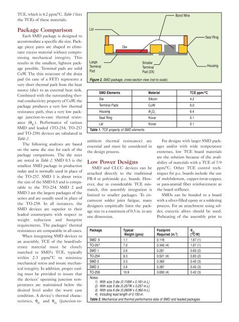
Package Comparison<br />
Each <strong>SMD</strong> package is designed to<br />
accommodate a specific die size. Package<br />
piece parts are shaped to eliminate<br />
excess material without compromising<br />
mechanical integrity. This<br />
results in the smallest, lightest package<br />
possible. Terminal pads are solid<br />
CuW. The thin structure of the drain<br />
pad (in case of a FET) represents a<br />
very short thermal path from the heat<br />
source (die) to an external heat sink.<br />
Combined with the outst<strong>and</strong>ing thermal<br />
conductivity property of CuW, the<br />
package produces a very low thermal<br />
resistance path, thus a very low package<br />
junction-to-case thermal resistance<br />
(θ JC<br />
). Performance of various<br />
<strong>SMD</strong> <strong>and</strong> leaded (TO-254, TO-257<br />
<strong>and</strong> TO-258) devices are tabulated in<br />
Table 2.<br />
The following analyses are based<br />
on the same die size for each of the<br />
package comparisons. The die sizes<br />
are noted in Table 2. <strong>SMD</strong> 0.5 is the<br />
smallest <strong>SMD</strong> package in production<br />
today <strong>and</strong> is normally used in place of<br />
the TO-257. <strong>SMD</strong> 1 is about twice<br />
the size of the <strong>SMD</strong> 0.5 <strong>and</strong> is comparable<br />
to the TO-254. <strong>SMD</strong> 2 <strong>and</strong><br />
<strong>SMD</strong> 3 are the largest packages of the<br />
series <strong>and</strong> are usually used in place of<br />
the TO-258. In all instances, the<br />
<strong>SMD</strong> devices are superior to their<br />
leaded counterparts with respect to<br />
weight reduction <strong>and</strong> footprint<br />
requirements. The packages’ thermal<br />
resistances are comparable in all cases.<br />
When integrating <strong>SMD</strong> devices to<br />
an assembly, TCE of the board/substrate<br />
material must be closely<br />
matched to <strong>SMD</strong>’s TCE, typically<br />
within 2-3 ppm/°C to minimize<br />
mechanical stress <strong>and</strong> insure mechanical<br />
integrity. In addition, proper cooling<br />
must be provided to insure that<br />
the devices’ operating junction temperatures<br />
are maintained below the<br />
desired level under the worst case<br />
condition. A device’s thermal characteristics,<br />
θ JC<br />
<strong>and</strong> θ JA<br />
(junction-to-<br />
Figure 2. <strong>SMD</strong> package, cross-section view (not to scale).<br />
<strong>SMD</strong> Elements Material TCE ppm/°C<br />
Die Silicon 4.2<br />
Terminal Pads CuW 6.0<br />
Housing Al 2<br />
O 3<br />
6.4<br />
Seal Ring Kovar 5.1<br />
Lid Kovar 5.1<br />
Table 1. TCE property of <strong>SMD</strong> elements.<br />
ambient thermal resistance) are<br />
essential <strong>and</strong> must be considered in<br />
the design process.<br />
Low Power Designs<br />
<strong>SMD</strong> <strong>and</strong> CLCC devices can be<br />
attached directly to the traditional<br />
FR-4 or polyimide p.c. boards. However,<br />
due to considerable TCE mismatch,<br />
this assembly integration is<br />
limited to smaller packages. To circumvent<br />
solder joint fatigue, many<br />
designers empirically limit the package<br />
size to a maximum of 0.5 in. in any<br />
one dimension.<br />
For designs with larger <strong>SMD</strong> packages<br />
<strong>and</strong>/or with wide temperature<br />
extremes, low TCE board materials<br />
are the solution because of the availability<br />
of materials with a TCE of 7-9<br />
ppm/°C. Other TCE control techniques<br />
for p.c. boards include the use<br />
of molybdenum, copper-invar-copper,<br />
or para-aramid fiber reinforcement as<br />
the board stiffener.<br />
<strong>SMD</strong>s can be bonded to a board<br />
with a silver-filled epoxy or a soldering<br />
process. For an attachment using solder,<br />
eutectic alloys should be used.<br />
Preheating of the assembly prior to<br />
Package Typical Footprint θ JC<br />
Weight (gms) Required (in. 2 ) (°C/W)<br />
<strong>SMD</strong> .5 1.1 0.118 1.67 (1)<br />
TO-257 7.0 0.340 (4) 1.67 (1)<br />
<strong>SMD</strong> 1 2.6 0.281 0.83 (2)<br />
TO-254 9.3 0.521 (4) 0.83 (2)<br />
<strong>SMD</strong> 2 3.3 0.362 0.42 (3)<br />
<strong>SMD</strong> 3 3.4 0.387 0.42 (3)<br />
TO-258 10.9 0.693 (4) 0.42 (3)<br />
Notes:<br />
1) With size 3 die (0.116W x 0.181-in.L)<br />
2) With size 5 die (0.257W x 0.257-in.L)<br />
3) With size 6 die (0.260W x 0.360-in.L)<br />
4) Including lead length of 0.150-in.<br />
Table 2. Mechanical <strong>and</strong> thermal performance data of <strong>SMD</strong> <strong>and</strong> leaded packages.


