

New Materials and Technologies Solve Hermetic SMD Integration
New Materials and Technologies Solve Hermetic SMD Integration
New Materials and Technologies Solve Hermetic SMD Integration

Create successful ePaper yourself
Turn your PDF publications into a flip-book with our unique Google optimized e-Paper software.
Figure 3. <strong>SMD</strong> with Leads.<br />
soldering <strong>and</strong> allowing the assembly to<br />
cool naturally after a soldering process<br />
are highly recommended. Exposing<br />
<strong>SMD</strong> components to higher than<br />
300°C may cause permanent damage.<br />
Because FR-4 <strong>and</strong> polyimide board<br />
materials are poor thermal conductors,<br />
the p.c. board should not be considered<br />
as a thermal medium or heat<br />
spreader unless its copper traces are<br />
sufficiently large. Otherwise, cooling<br />
the semiconductor relies almost<br />
entirely on the package’s ability to<br />
dissipate thermal losses in the free<br />
convection environment. The package’s<br />
θ JA<br />
then becomes the key design<br />
parameter.<br />
For the aerospace environment<br />
where convection is nonexistent <strong>and</strong><br />
radiation cooling is minimal, conduction<br />
is the only meaningful cooling<br />
method. For cooling, it may be necessary<br />
to attach an <strong>SMD</strong> to an on-board<br />
heat spreader or an enlarged copper<br />
trace.<br />
For a device dissipating 1W with θ JA<br />
of 25°C/W, the junction temperature<br />
equals 100°C for an 75°C ambient.<br />
This is based on:<br />
(<br />
P = T J − T A )<br />
D<br />
θ<br />
JA<br />
(1)<br />
Where:<br />
P D<br />
= Device power dissipation<br />
T J<br />
= Operating junction temperature<br />
T A<br />
= Ambient temperature<br />
θ JA<br />
= Package junction-to-ambient<br />
thermal resistance<br />
High Power Designs<br />
For high-power applications where<br />
<strong>SMD</strong> devices dissipate more than a<br />
few watts <strong>and</strong> must be cooled with a<br />
heat sink, there are three basic assembly<br />
integration techniques. One<br />
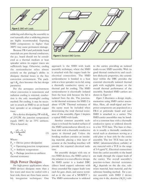
Figure 4. St<strong>and</strong>ard <strong>SMD</strong> Carriers.<br />
approach is the <strong>SMD</strong> with leads<br />
assembly technique, where the <strong>SMD</strong><br />
is attached with flat copper leads for<br />
electrical connections. The <strong>SMD</strong><br />
semiconductor is bonded to a heat<br />
sink or a heat spreader via its lid, using<br />
a thermally conductive epoxy or a<br />
thermal pad for cooling. The <strong>SMD</strong><br />
semiconductor is electrically isolated<br />
from the heat sink because the lid is<br />
isolated from the die. The junctionto-lid<br />
thermal resistance for <strong>SMD</strong> 2 is<br />
about 6°C/W. Thermal resistance of<br />
the epoxy must be included when<br />
determining the total thermal resistance<br />
of the assembly. Figure 3 depicts<br />
a typical <strong>SMD</strong> with leads.<br />
Another common assembly technique<br />
is to bond the leaded surfaces of<br />
the <strong>SMD</strong> semiconductor directly to a<br />
heat sink with a thermally conductive<br />
epoxy or thermal pad. Unless the<br />
bonding medium contains an insulating<br />
material, placing a thin layer of<br />
ceramic at the bonding interface will<br />
provide the required electrical isolation.<br />
For assembly designs with one or<br />
two <strong>SMD</strong> devices, the <strong>SMD</strong> carrier is<br />
the solution to a cost-effective design.<br />
An <strong>SMD</strong> carrier is a leaded DBC<br />
(direct bond copper) substrate with<br />
three extended flat copper leads (one<br />
each for gate, drain, <strong>and</strong> source terminal<br />
as in the case of a MOSFET ).<br />
The <strong>SMD</strong> semiconductor is soldered<br />
to the carrier, providing an isolated<br />
ready-to-use <strong>SMD</strong> assembly. With its<br />
good thermal conductivity <strong>and</strong> excellent<br />
dielectric properties, the ceramic<br />
layer within the DBC provides the<br />
essential electrically isolated thermal<br />
path with negligible impact on the<br />
overall thermal performance of the<br />
assembly. St<strong>and</strong>ard <strong>SMD</strong> carriers are<br />
shown in Figure 4.<br />
Figure 5 illustrates a design implementation<br />
using <strong>SMD</strong> carrier assemblies.<br />
Here, all small-signal <strong>and</strong> lowpower<br />
components are populated on a<br />
FR-4 or polyimide board <strong>and</strong> each<br />
<strong>SMD</strong> is attached to a carrier. The<br />
<strong>SMD</strong> carrier assemblies may be bonded<br />
to a common base with a thermally<br />
conductive epoxy or soldered directly<br />
to a low TCE base. The base or chassis<br />
is usually a thermally conductive<br />
metal such as aluminum serving as a<br />
cold plate or heat sink for the entire<br />
assembly. The low TCE base can be<br />
Al/SiC (aluminum/silicon carbide) or<br />
any material with a TCE in the range<br />
of 5-9 ppm/°C. Electrical connections<br />
from the carrier assembly to the board<br />
are made through the copper leads of<br />
the carrier. The overall assembly’s<br />
junction-to-base thermal resistance<br />
(θ JB<br />
) depends on the die size, substrate<br />
material, base material, <strong>and</strong> the<br />
substrate bonding method. For a carrier<br />
assembly with <strong>SMD</strong> 2 device<br />
using size 6 die, alumina (Al 2<br />
O 3<br />
) sub-


