

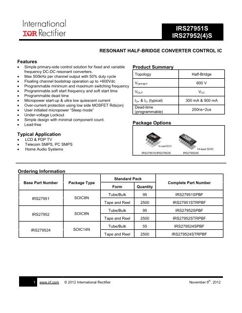
IRS27951S IRS27952(4)S - International Rectifier
IRS27951S IRS27952(4)S - International Rectifier
IRS27951S IRS27952(4)S - International Rectifier

You also want an ePaper? Increase the reach of your titles
YUMPU automatically turns print PDFs into web optimized ePapers that Google loves.
<strong>IRS27951S</strong><br />
<strong>IRS27952</strong>(4)S<br />
RESONANT HALF-BRIDGE CONVERTER CONTROL IC<br />
Features<br />
• Simple primary-side control solution for fixed and variable<br />
frequency DC-DC resonant converters.<br />
• Max 500kHz per channel output with 50% duty cycle<br />
• Floating channel bootstrap operation up to +600Vdc<br />
• Programmable minimum and maximum switching frequency<br />
• Programmable soft start frequency and soft start time<br />
• Programmable dead time<br />
• Micropower start-up & ultra low quiescent current<br />
• Over-current protection using low side MOSFET Rds(on)<br />
• User initiated micropower “Sleep mode”<br />
• Under-voltage Lockout<br />
• Simple design with minimal component count.<br />
• Lead-free<br />
Product Summary<br />
Topology<br />
V OFFSET<br />
V OUT<br />
I O+ & I O- (typical)<br />
Dead-time<br />
(programmable)<br />
Package Options<br />
Half-Bridge<br />
600 V<br />
V CC<br />
300 mA & 900 mA<br />
200ns~2us<br />
Typical Application<br />
• LCD & PDP TV<br />
• Telecom SMPS, PC SMPS<br />
• Home Audio Systems<br />
<strong>IRS27951S</strong>/<strong>IRS27952</strong>S<br />
14-lead SOIC<br />
<strong>IRS27952</strong>4S<br />
Ordering Information<br />
Base Part Number<br />
Package Type<br />
Standard Pack<br />
Form<br />
Quantity<br />
Complete Part Number<br />
IRS27951<br />
<strong>IRS27952</strong><br />
<strong>IRS27952</strong>4<br />
SOIC8N<br />
SOIC8N<br />
SOIC14N<br />
Tube/Bulk 95 <strong>IRS27951S</strong>PBF<br />
Tape and Reel 2500 <strong>IRS27951S</strong>TRPBF<br />
Tube/Bulk 95 <strong>IRS27952</strong>SPBF<br />
Tape and Reel 2500 <strong>IRS27952</strong>STRPBF<br />
Tube/Bulk 55 <strong>IRS27952</strong>4SPBF<br />
Tape and Reel 2500 <strong>IRS27952</strong>4STRPBF<br />
1 www.irf.com © 2012 <strong>International</strong> <strong>Rectifier</strong> November 8 th , 2012
<strong>IRS27951S</strong><br />
<strong>IRS27952</strong>(4)S<br />
Typical Application Diagram<br />
VIN<br />
DC BUS<br />
R1<br />
R2<br />
Dbs<br />
Rcc<br />
D3<br />
Dss<br />
Rss<br />
RT<br />
CDC<br />
1<br />
2<br />
3<br />
4<br />
U1<br />
VCC<br />
RT<br />
CT/SD<br />
COM<br />
IRS2795<br />
VB 8<br />
HO 7<br />
VS 6<br />
LO 5<br />
Cbs<br />
Rg1<br />
Rg2<br />
M1<br />
M2<br />
Lr<br />
D1<br />
Rmax<br />
Css<br />
CT<br />
COUT<br />
LOAD<br />
Cr<br />
D2<br />
RTN<br />
Rled<br />
U2<br />
Rbias<br />
Cf 2<br />
Cf 1<br />
Rf 2<br />
Rs1<br />
U3<br />
TL431<br />
Rs2<br />
2 www.irf.com © 2012 <strong>International</strong> <strong>Rectifier</strong> November 8 th , 2012
Table of Contents<br />
<strong>IRS27951S</strong><br />
<strong>IRS27952</strong>(4)S<br />
Ordering Information 1<br />
Typical Application Diagram 2<br />
Absolute Maximum Ratings 5<br />
Recommended Operating Conditions 5<br />
Electrical Characteristics 6<br />
Functional Block Diagram 8<br />
Input/Output Pin Equivalent Circuit Diagram 9<br />
Lead Definitions 10<br />
Lead Assignments 10<br />
State Diagram 12<br />
Application Information and Additional Details 13<br />
Package Details 23<br />
Tape and Reel Details 25<br />
Part Marking Information 27<br />
Qualification Information 28<br />
Page<br />
3 www.irf.com © 2012 <strong>International</strong> <strong>Rectifier</strong> November 8 th , 2012
<strong>IRS27951S</strong><br />
<strong>IRS27952</strong>(4)S<br />
Description<br />
The IRS2795(1,2)(4) is a self oscillating half-bridge driver IC for DC-DC resonant converter applications, especially<br />
the LLC resonant half-bridge converter. The frequency and dead time can be programmed externally using two<br />
external components. The IC offers over current protection using the on state resistance of the low-side MOSFET.<br />
The IC can be disabled by externally pulling the voltage at the CT/SD pin below its enable voltage threshold<br />
4 www.irf.com © 2012 <strong>International</strong> <strong>Rectifier</strong> November 8 th , 2012
<strong>IRS27951S</strong><br />
<strong>IRS27952</strong>(4)S<br />
Absolute Maximum Ratings<br />
Absolute maximum ratings indicate sustained limits beyond which damage to the device may occur. All voltage<br />
parameters are absolute voltages referenced to COM, all currents are defined positive into any lead. The thermal<br />
resistance and power dissipation ratings are measured under board mounted and still air conditions.<br />
Symbol Definition Min. Max. Units<br />
V CC Supply Voltage -0.3 25<br />
V B High-side Floating Supply Voltage -0.3 625<br />
V S High-side Floating Supply Offset Voltage V B – 25 V B + 0.3<br />
V HO High-side Floating Output Voltage V S – 0.3 V B + 0.3 V<br />
V LO Low-side Output Voltage -0.3 V CC + 0.3<br />
V CT CT/SD Pin Voltage -0.3 V CC + 0.3<br />
V RT RT Pin Voltage -0.3 V CC + 0.3<br />
I RT RT pin source current --- 2 mA<br />
dV s /dt Allowable offset voltage slew rate -50 50 V/ns<br />
T J Operating Junction Temperature -40 150<br />
T S Storage Temperature -55 150<br />
°C<br />
P D<br />
Package power dissipation @ TA ≤ (8 lead SOIC) — 0.833<br />
25°C<br />
(14 lead SOIC) — 1.04<br />
W<br />
Rth JA<br />
Thermal resistance, junction to<br />
(8 lead SOIC) — 150<br />
ambient<br />
(14 lead SOIC) — 120<br />
°C/W<br />
Recommended Operating Conditions<br />
For proper operation the device should be used within the recommended conditions.<br />
Symbol Definition Min. Max. Units<br />
V BS High-side floating supply voltage 10 Vcc<br />
V S Steady-state high-side floating supply offset voltage -3.0 † 600 V<br />
V CC Supply voltage 12 18<br />
fsw Switching Frequency --- 500 kHz<br />
† Care should be taken to avoid output switching conditions where the VS node flies inductively below ground by<br />
more than 5 V.<br />
Recommended Component Values<br />
Symbol Component Min. Max. Units<br />
R RT RT pin resistor value 2 100 kΩ<br />
C CT CT pin capacitor value 200 2000 pF<br />
5 www.irf.com © 2012 <strong>International</strong> <strong>Rectifier</strong> November 8 th , 2012
<strong>IRS27951S</strong><br />
<strong>IRS27952</strong>(4)S<br />
Electrical Characteristics<br />
VCC=VBS=15V, VS=0V, CVCC=CBS=0.1uF, CLO=CHO=1nF, RT=50.5kΩ, CT=200pF and TA = 25°C unless<br />
otherwise specified. The output voltage and current (VO and IO) parameters are referenced to COM and are<br />
applicable to the respective HO and LO output leads.<br />
Symbol Definition Min Typ Max Units Test Conditions<br />
Low Voltage Supply Characteristics<br />
V CCUV+ V CC turn on threshold 10.1 11 11.9<br />
V CCUV-<br />
V CC turn off threshold<br />
(Under Voltage Lock Out)<br />
8.1 9 9.9<br />
V CCUVHYS V CC undervoltage lockout hysteresis --- 2 ---<br />
V<br />
N/A<br />
I CCSTART V CC startup current --- 50 100<br />
V CC = V CCUV+<br />
µA<br />
-0.1V<br />
I SLEEP Sleep mode V CC supply current --- 150 200 V CT/SD<br />
<strong>IRS27951S</strong><br />
<strong>IRS27952</strong>(4)S<br />
Electrical Characteristics<br />
VCC=VBS=15V, VS=0V, CVCC=CBS=0.1uF, CLO=CHO=1nF, RT=50.5kΩ, CT=200pF and TA = 25°C unless<br />
otherwise specified. The output voltage and current (VO and IO) parameters are referenced to COM and are<br />
applicable to the respective HO and LO output leads.<br />
Symbol Definition Min Typ Max Units Test Conditions<br />
Protection Characteristics<br />
R RTD RT discharge resistance --- 115 ---<br />
R CTD CT/SD discharge resistance --- 115 ---<br />
Ω<br />
V EN1 CT/SD rising enable voltage 0.75 1.05 1.4<br />
V EN2 CT/SD standby voltage 0.6 0.85 1.1 V<br />
V ENHYST CT/SD enable hysteresis voltage --- 0.2 ---<br />
V OCP Overcurrent VS threshold<br />
1.9 2 2.1<br />
IRS27951<br />
V<br />
2.85 3 3.15 <strong>IRS27952</strong>(4)<br />
t BLANK Leading edge blanking on LO --- 300 ---<br />
GBD<br />
ns<br />
t SD Shutdown propagation delay --- 300 --- GBD<br />
Gate Driver Output Characteristics<br />
V OH Gate High Voltage Vcc-1 --- ---<br />
I GATE = 20mA<br />
V<br />
V OL Gate Low Voltage --- 0.05 0.15 I GATE = -20mA<br />
t r Output rise time --- 60 ---<br />
C LOAD =1nF<br />
t r Output rise time --- 200 --- C LOAD =4.7nF<br />
ns<br />
t f Output fall time --- 16 --- C LOAD =1nF<br />
t f Output fall time --- 65 --- C LOAD =4.7nF<br />
M DT<br />
Output deadtime matching<br />
|(DTLO-HO) – (DTHO-LO)|<br />
--- --- 25 ns<br />
I O+ Output source current --- 300 ---<br />
I O- Output sink current --- 900 ---<br />
mA GBD<br />
R UP Pull up Resistance --- 20 ---<br />
I<br />
Ω GATE = 20mA<br />
R DOWN Pull down Resistance --- 3 --- I GATE =-20mA<br />
† GBD: Guaranteed by design.<br />
7 www.irf.com © 2012 <strong>International</strong> <strong>Rectifier</strong> November 8 th , 2012
<strong>IRS27951S</strong><br />
<strong>IRS27952</strong>(4)S<br />
Functional Block Diagram<br />
VB<br />
dv/DT<br />
BOOSTER<br />
UVBS<br />
RT<br />
2V<br />
+<br />
-<br />
CURRENT FAULT LOGIC<br />
& CONTROL<br />
HV LEVEL<br />
SHIFTER<br />
S<br />
R<br />
Q<br />
Q<br />
HO<br />
VS<br />
Dead Time<br />
CT/SD<br />
OSCILLATOR<br />
PULSE STEERING<br />
UV DETECTION<br />
VCC<br />
DELAY<br />
MATCH<br />
LO<br />
SLEEP MODE LOGIC<br />
COM<br />
8 www.irf.com © 2012 <strong>International</strong> <strong>Rectifier</strong> November 8 th , 2012
<strong>IRS27951S</strong><br />
<strong>IRS27952</strong>(4)S<br />
Input/Output Pin Equivalent Circuit Diagrams:<br />
VCC<br />
VB<br />
RT<br />
ESD<br />
Diode<br />
ESD<br />
Diode<br />
RESD<br />
HO<br />
ESD<br />
Diode<br />
ESD<br />
Diode<br />
25V<br />
COM<br />
VS<br />
600V<br />
VCC<br />
VCC<br />
ESD<br />
Diode<br />
ESD<br />
Diode<br />
CT<br />
ESD<br />
Diode<br />
RESD<br />
RESD<br />
LO<br />
ESD<br />
Diode<br />
25V<br />
COM<br />
COM<br />
9 www.irf.com © 2012 <strong>International</strong> <strong>Rectifier</strong> November 8 th , 2012
<strong>IRS27951S</strong><br />
<strong>IRS27952</strong>(4)S<br />
Lead Definitions:<br />
Symbol<br />
VCC<br />
RT<br />
CT/SD<br />
COM<br />
LO<br />
VS<br />
HO<br />
VB<br />
Description<br />
Supply Voltage<br />
Oscillator timing resistor<br />
Oscillator timing capacitor / shutdown<br />
Ground<br />
Low-side gate drive<br />
High-side gate drive return / HV current Sense<br />
High-side gate drive<br />
High-side floating supply voltage<br />
Lead Assignments: IRS2795(1,2)S<br />
1<br />
VCC<br />
VB<br />
8<br />
2<br />
RT<br />
HO<br />
7<br />
3<br />
CT/SD<br />
VS<br />
6<br />
4<br />
COM<br />
LO<br />
5<br />
Lead Assignments: <strong>IRS27952</strong>4S<br />
1<br />
NC<br />
NC<br />
14<br />
2<br />
VCC<br />
VB<br />
13<br />
3<br />
RT<br />
HO<br />
12<br />
4<br />
CT/SD<br />
VS<br />
11<br />
5<br />
COM<br />
NC<br />
10<br />
6<br />
NC<br />
NC<br />
9<br />
7<br />
NC<br />
LO<br />
8<br />
10 www.irf.com © 2012 <strong>International</strong> <strong>Rectifier</strong> November 8 th , 2012
<strong>IRS27951S</strong><br />
<strong>IRS27952</strong>(4)S<br />
VCC: Power Supply Voltage<br />
This is the supply voltage pin of the IC and sense node for the under-voltage lock out circuit. It is possible to turn off<br />
the IC by pulling this pin below the minimum turn off threshold voltage, V CCUV- without damage to the IC. This pin is<br />
not internally clamped.<br />
RT: Oscillator timing resistor<br />
This pin provides a precise 2V reference and a resistor connected from this pin to COM defines a current that is<br />
used to set the minimum oscillator frequency. To close the feedback loop that regulates the converter output<br />
voltage by modulating the oscillator frequency, the phototransistor of an optocoupler will be connected to this pin<br />
through a resistor. The value of this resistor will set the maximum operating frequency. An R-C series connected<br />
from this pin to COM sets frequency shift at start-up to prevent excessive energy inrush (soft-start).<br />
CT/SD: Oscillator timing capacitor /Shutdown<br />
An external capacitor CT from this pin to COM sets the dead time and frequency of the oscillator. The CT pin has<br />
sawtooth waveform, which is charged up by the current reference programmed at RT pin during rising slope and is<br />
discharged by an internal fixed 2mA current source during the falling slope. The falling time of the sawtooth defines<br />
the dead-time.<br />
At start-up, a 10uA current source charges this capacitor and the oscillator is enabled only when the voltage at this<br />
pin exceeds VEN1. The IC can also be used to enter sleep mode by externally pulling this pin below VEN2.<br />
COM: Logic and Gate drive Ground<br />
This is ground potential pin of the integrated control circuit. All internal circuits are referenced to this point.<br />
LO: Low-side Gate Drive Output<br />
The driver is capable of 0.3A source and 0.9A sink peak current to drive the lower MOSFET of the half-bridge leg.<br />
The pin is actively pulled to GND during UVLO.<br />
VS: High Side Gate Return/Current Sense<br />
This is the floating supply return. This pin also acts as a high voltage current sense pin and uses the low-side<br />
MOSFET R DSON to detect an over current fault condition.<br />
HO: High-side Gate Drive<br />
The driver is capable of 0.3A source and 0.9A sink peak current to drive the high-side MOSFET in the half-bridge. A<br />
resistor internally connected to pin VS ensures that the pin is not floating during UVLO.<br />
VB: High Side floating supply voltage<br />
The bootstrap capacitor connected between this pin and VS is charged by the bootstrap diode when the low-side<br />
gate-drive is high.<br />
11 www.irf.com © 2012 <strong>International</strong> <strong>Rectifier</strong> November 8 th , 2012
<strong>IRS27951S</strong><br />
<strong>IRS27952</strong>(4)S<br />
State Diagram<br />
DC POWER ON<br />
Gate Inactive<br />
Oscillator Inactive<br />
VCC < VCCUV-<br />
UVLO<br />
Oscillator Inactive<br />
Gates Inactive<br />
VCC < VCCUV-<br />
VCC > VCCUV+<br />
CURRENT FAULT<br />
Oscillator and Gates Inactive<br />
Internally discharge RT and CT pins<br />
SLEEP<br />
Oscillator and Gates Inactive<br />
ICT = ICTSTART<br />
ICC=ISLEEP<br />
VCT < VEN2<br />
VCT > VEN1<br />
NORMAL<br />
VS > VOCP<br />
@ LO=High<br />
Oscillator and Gates Active<br />
ICTCHARGE=IRT<br />
Over Current Protection Active<br />
UVLO Mode<br />
The IC remains in the UVLO condition until the voltage on the V CC pin exceeds the V CC turn on threshold voltage,<br />
V CCUV+. During the time the IC remains in the UVLO state, the gate drive circuit is inactive and the IC draws a<br />
quiescent current of I CC START . The UVLO mode is accessible from any other state of operation whenever the IC<br />
supply voltage condition of V CC < V CC UV- occurs.<br />
Sleep Mode<br />
When V CC exceeds the V CCUV+ threshold the IRS2795(1,2)(4) starts to charge up CT capacitor with I CT startup<br />
current towards the enable threshold, V EN1 . During this period, the IC is in Sleep mode. The oscillator and gate<br />
drive circuits are disabled and the Ic consumes I SLEEP .<br />
When the voltage at the CT/SD pin exceeds V EN1 , the IC is pulled out of sleep mode and the 2V reference voltage<br />
at the RT pin is enabled.<br />
The IC can be placed in Sleep mode while operating in Normal mode by externally pulling the CT/SD pin below<br />
V EN2 . When this occurs, the RT pin of the IC is internally discharged to COM to ensure a system restart with softstart.<br />
Normal Mode<br />
The IC enters in normal operating mode once the UVLO voltage and V EN1 has been exceeded. The RT pin<br />
voltage is 2V under normal mode. Gate drive signal appears at HO and LO with fixed 50% duty-cycle.<br />
During this mode, the over-current protection scheme using the VS sense circuitry is active.<br />
Current Fault Mode<br />
When operating in Normal mode, the IC senses the voltage on the VS pin each time the low-side device is turned<br />
ON (with a leading edge blanking on LO, t blank ). When the voltage sensed exceeds VOCP, the IC terminates the<br />
current gate pulse, disables the oscillator and gate drivers, and enters the Current Fault mode. When the IC<br />
enters this state, RT and CT/SD pins are internally discharged and IC supply voltage must be recycled before the<br />
IC can restart with soft-start again<br />
12 www.irf.com © 2012 <strong>International</strong> <strong>Rectifier</strong> November 8 th , 2012
<strong>IRS27951S</strong><br />
<strong>IRS27952</strong>(4)S<br />
Application Information and Additional Details<br />
Information regarding the following topics is included as subsections within this section of the datasheet.<br />
• General Description<br />
• IC Supply Circuit & Low start-up current<br />
• Multi-function 2 Pin Oscillator<br />
• Frequency and Dead-time Calculation<br />
• User initiated Micropower Sleep mode<br />
• Gate Drive Capability<br />
• System Protection Features<br />
• PCB Layout Tips<br />
• Additional Documentation<br />
General Description<br />
The IRS2795(1,2)(4) is a double-ended controller for the resonant half-bridge topology. It provides complementary<br />
outputs with 50% (max) duty cycle; the high-side and low-side bridge devices are driven 180° out-of-phase for<br />
exactly the same time. A programmable dead-time inserted between the turn-OFF of one switch and the turn-ON of<br />
the other one guarantees soft-switching operation. The IC incorporates a multi-function oscillator that allows the<br />
designer to program all the necessary features to control a half bridge resonant switch-mode power supply featuring<br />
low standby power. The IC also incorporates additional protection features for robust operation and provides a high<br />
performance solution while minimizing external components, design time, and printed circuit board real estate.<br />
The IC enables the designer to externally program all the following features using a 2 pin RC oscillator – operating<br />
frequency range (start-up, minimum and maximum frequency), dead time, soft-start time and sleep mode operation.<br />
IRS2795(1,2)(4) also uses IR’s proprietary high-voltage technology to implement a VS sensing circuitry that<br />
monitors the current through the low-side half bridge MOSFET for short circuit faults. By using the R DSON of the lowside<br />
MOSFET, the IRS2795(1,2)(4) eliminates the need for an additional current sensing resistor, filter and currentsensing<br />
pin. This protection feature is latched and the thresholds are fixed at 2V for IRS27951 and 3V for<br />
<strong>IRS27952</strong>(4).<br />
Finally, the controller IC also features a micro power startup current (ICC
<strong>IRS27951S</strong><br />
<strong>IRS27952</strong>(4)S<br />
Multi-function 2 Pin Oscillator<br />
The two pin oscillator is externally programmed by a resistor RT connected between pin#2 and COM and a<br />
capacitor CT, connected from pin#3 to COM. The RT pin provides an accurate 2V reference (±2%) with a 2mA<br />
source capability (higher the current sourced by the pin, the higher is the oscillator frequency).<br />
In normal operation, CT is charged by a current defined by the network connected at the RT pin. The oscillator ramp<br />
charges and discharges between the two ramp thresholds (3 and 5V). When the ramp voltage reaches 5V, it is<br />
internally discharged by a fixed current of 2mA. The fall time for the ramp corresponds to the dead time between the<br />
bridge devices.<br />
At startup, a 10uA internal current source charges the oscillator capacitor at the CT pin to V EN1 . At this point, the IC<br />
is pulled out of sleep mode and the 2V reference voltage at the RT pin is enabled. The low-side device is now also<br />
turned ON to charge the bootstrap capacitor (this sequence at startup or while exiting sleep mode ensures that the<br />
low-side device is always switched on first to charge the bootstrap capacitor which will be ready to supply the highside<br />
floating driver). The low-side device remains ON till the CT pin voltage reaches the upper ramp threshold of 5V<br />
(see Fig 2).<br />
The programmable features for the oscillator are listed below-<br />
• Wide frequency range:<br />
The high-speed oscillator allows an output frequency from 50 kHz up to 500 kHz.<br />
• Programmable dead-time:<br />
The oscillator timing capacitor CT also programs the dead time between LO and HO.<br />
• Programmable soft-start time:<br />
In resonant converter applications, the output power delivered is an inverse function of frequency i.e. soft- start is<br />
achieved by sweeping the operating frequency from an initial high value until the control loop takes over.<br />
Additionally, the resonant tank has a non-linear frequency dependence that makes the converter’s power transfer<br />
capability change little when the frequency is away from resonance and change very quickly as frequency<br />
approaches the resonant tank frequency.<br />
An R-C series circuit (CSS + RSS) connected between the RT pin and COM programs the soft-start time for the<br />
converter. Initially, the capacitor CSS is totally discharged, so that the series resistor RSS is effectively in parallel to<br />
Rfmin and the resulting initial frequency is determined by RSS and RT only (the optocoupler’s phototransistor is cut<br />
off). During this frequency sweep, the operating frequency will decay following the exponential charge of CSS, that<br />
is, initially it will change relatively quickly but the rate of change will get slower. The CSS capacitor charges until its<br />
voltage reaches 2V and, consequently, the current through RSS is reduced to zero.<br />
The soft-start sequence is activated at normal startup and back to operation from Sleep mode.<br />
• Programmable start-up, minimum and maximum frequency:<br />
In resonant converter applications, it is important to operate the converter in the soft-switching region of operation.<br />
IRS2795(1,2)(4) offers a trimmed voltage reference (±2%) at the RT pin to accurately program the converter<br />
switching frequency range in the desired region of operation.<br />
- The effective resistance (RSS//RT) at pin#2 during IC power up and the CT capacitor program the start-up<br />
frequency of the converter.<br />
- RT and CT program the minimum operating frequency.<br />
14 www.irf.com © 2012 <strong>International</strong> <strong>Rectifier</strong> November 8 th , 2012
<strong>IRS27951S</strong><br />
<strong>IRS27952</strong>(4)S<br />
- For closed loop systems with feedback control, a resistor Rfmax can be connected between the RT<br />
pin and the collector of the (emitter-grounded) phototransistor. The feedback loop modulates the<br />
current through the phototransistor and hence, the oscillator frequency for output voltage regulation.<br />
- The converter maximum frequency is set by (Rmax//RT) and CT.<br />
VCCON<br />
VCC<br />
2V<br />
RT<br />
5V<br />
CT<br />
3V<br />
VEN1<br />
HO<br />
LO<br />
UVLO<br />
SLEEP<br />
NORMAL<br />
Figure 2: Typical startup waveforms with soft-start<br />
Frequency and Dead-time Calculation<br />
The dead time is calculated by the following equation:<br />
t<br />
DT<br />
2V<br />
= ( 0.85CT<br />
+ 40 pF)<br />
⋅<br />
2mA<br />
15 www.irf.com © 2012 <strong>International</strong> <strong>Rectifier</strong> November 8 th , 2012
<strong>IRS27951S</strong><br />
<strong>IRS27952</strong>(4)S<br />
Dead-Time vs. CT Value<br />
DT (ns)<br />
2000<br />
1800<br />
1600<br />
1400<br />
1200<br />
1000<br />
800<br />
600<br />
400<br />
200<br />
0<br />
0 500 1000 1500 2000<br />
CT (pF)<br />
Figure 3: Dead-time with CT capacitor chart<br />
The running frequency of the IRS2795(1,2)(4) is given by:<br />
f<br />
SW<br />
=<br />
2 ⋅[<br />
R<br />
Teq<br />
1<br />
(0.85C<br />
+ 40 pF)<br />
+ t<br />
T<br />
DT<br />
]<br />
R Teq is the total equivalent resistance at RT pin.<br />
Or just simply select the RT value form the frequency chart shown below:<br />
Frequency Chart<br />
Frequency (KHz)<br />
500<br />
450<br />
400<br />
350<br />
300<br />
250<br />
200<br />
150<br />
100<br />
50<br />
0<br />
CT=220pF<br />
CT=330pF<br />
CT=470pF<br />
CT=1nF<br />
0 10 20 30 40 50<br />
RT (KΩ)<br />
Figure 4: Switching frequency and RT selection<br />
The maximum duty cycle is given by:<br />
DC<br />
MAX<br />
= 0.5<br />
− ( t * f )<br />
DT<br />
16 www.irf.com © 2012 <strong>International</strong> <strong>Rectifier</strong> November 8 th , 2012
<strong>IRS27951S</strong><br />
<strong>IRS27952</strong>(4)S<br />
User initiated Micro Power Sleep mode<br />
The IC can be actively pushed into a micropower sleep mode where current consumption is less than 200uA by<br />
pulling the CT pin below the sleep threshold V EN2 , even while the IC VCC is above VCCON. This mode allows the<br />
user to disable the resonant power converter during application standby modes in order to meet regulation<br />
standards (Blue Angel, Energy Start, Green Power etc). This IC disabling feature can also be use to implement<br />
other system protection features.<br />
5V<br />
CT<br />
3V<br />
VEN2<br />
HO<br />
LO<br />
2V<br />
RT<br />
NORMAL<br />
SLEEP<br />
Figure 5: IC transition from normal to sleep mode by pulling down CT/SD pin<br />
Gate Drive Capability<br />
The gate drive output stage of the IC is capable of 0.3A peak source current and 0.9A peak sink current drive<br />
capability. Gate drive buffer circuits can be easily driven with the GATE pin of the IC to adapt to any system power<br />
level.<br />
System Protection Features<br />
IRS2795(1,2)(4) uses IR’s high-voltage technology to implement a VS sensing circuitry that monitors the current<br />
through the low-side half bridge MOSFET for short circuit faults. By using the R DSON of the low-side MOSFET, the<br />
need for an additional current sensing resistor is eliminated. The voltage at the VS node is sensed after a leading<br />
edge blanking time on LO. When the sensed voltage exceeds the protection thresholds, the IC enters Current<br />
Fault Mode (gate drive outputs are disabled and the oscillator pins are internally discharged to COM).<br />
This protection feature is latched and the IC supply voltage must be pulled below the UVLO threshold and then<br />
again above VCCON in order to reset the latch and restart the IC.<br />
17 www.irf.com © 2012 <strong>International</strong> <strong>Rectifier</strong> November 8 th , 2012
<strong>IRS27951S</strong><br />
<strong>IRS27952</strong>(4)S<br />
LO<br />
HO<br />
VS<br />
ILr<br />
VS Sensing Voltage<br />
OCP threshold<br />
VS Sensing is enabled when LO is high<br />
Figure 6: VS sensing over current protection<br />
PCB Layout Tips<br />
Distance between high and low voltage components: It is strongly recommended to place the components tied to<br />
the floating voltage pins (V B and V S ) near the respective high voltage portions of the device.<br />
Ground Plane: In order to minimize noise coupling, the ground plane should not be placed under or near the high<br />
voltage floating side.<br />
Gate Drive Loops: Current loops behave like antennas and are able to receive and transmit EM noise. In order to<br />
reduce the EM coupling and improve the power switch turn on/off performance, the gate drive loops must be<br />
reduced as much as possible. For the low-side driver, the return of the drive loop must be directly connected to the<br />
COM pin of the IC and separate with signal ground (power ground and signal ground have star connection at COM<br />
pin).<br />
Supply Capacitor: It is recommended to place a bypass capacitor (C IN ) between the V CC and COM pins. A 1μF<br />
ceramic capacitor is suitable for most applications. This component should be placed as close as possible to the<br />
pins in order to reduce parasitic elements.<br />
C BS Capacitor: The C BS capacitor should be placed as close as possible to the VB and VS pins.<br />
Routing and Placement: 1) The IC has only one COM pin for both signal return and power return, so it is strongly<br />
recommended to route the signal ground and power ground separately and with a star connection at the COM pin.<br />
2) The RT pin provides a current reference for the internal oscillator and needs to be kept as clean as possible to<br />
avoid frequency jittering or duty-cycle mismatch between high-side and low-side. The components connected to this<br />
pin must keep away from the high frequency switching loop such as the gate driver loop and the VS node. The PCB<br />
traces connected to RT pin also need to be kept away from any switching node. 3) Connect CT capacitor directly to<br />
COM pin, don’t share the return with any other signal ground.<br />
18 www.irf.com © 2012 <strong>International</strong> <strong>Rectifier</strong> November 8 th , 2012
<strong>IRS27951S</strong><br />
<strong>IRS27952</strong>(4)S<br />
Layout Example:<br />
VS node<br />
Signal components are kept<br />
away from switching nodes<br />
Supply bypass capacitors<br />
are close to IC pins.<br />
Star connection at COM pin<br />
Additional Documentation<br />
Please refer to application note AN-1160 for more design details of IRS2795(1,2)(4).<br />
Several technical documents related to the use of HVICs are also available at www.irf.com; use the Site Search<br />
function and the document number to quickly locate them. Below is a short list of some of these documents.<br />
AN-1160: Design of Resonant Half-Bridge converter using IRS2795(1,2) Control IC<br />
DT97-3: Managing Transients in Control IC Driven Power Stages<br />
19 www.irf.com © 2012 <strong>International</strong> <strong>Rectifier</strong> November 8 th , 2012
<strong>IRS27951S</strong><br />
<strong>IRS27952</strong>(4)S<br />
10<br />
12.0 V<br />
11.5 V<br />
I SUPPLY (mA)<br />
1<br />
0.1<br />
0.01<br />
5.0 V 7.5 V 10.0 V 12.5 V 15.0 V 17.5 V<br />
Supply voltage<br />
Figure 7: Supply Current vs. Supply Voltage<br />
VCC UVLO Thresholds<br />
11.0 V<br />
10.5 V<br />
10.0 V<br />
9.5 V<br />
9.0 V<br />
8.5 V<br />
VCC UV+<br />
VCC UV-<br />
8.0 V<br />
-50 °C 0 °C 50 °C 100 °C 150 °C<br />
Temperature<br />
Figure 8: Undervoltage Lockout vs. Temperature<br />
I QCC<br />
0.0<br />
I QCC Quiescent Current (mA)<br />
2.6<br />
2.4<br />
2.2<br />
2.0<br />
1.8<br />
1.6<br />
1.4<br />
1.2<br />
1.0<br />
-50 °C 0 °C 50 °C 100 °C 150 °C<br />
Temperature<br />
Current (uA)<br />
180.0<br />
160.0<br />
140.0<br />
120.0<br />
100.0<br />
80.0<br />
60.0<br />
40.0<br />
20.0<br />
I CCSTART and I SLEEP<br />
ISLEEP<br />
ICCSTART<br />
-50 °C 0 °C 50 °C 100 °C 150 °C<br />
Temperature<br />
Figure 9: Icc Quiescent Currrent vs. Temperature<br />
Figure 10: Startup Current and Sleep Current vs.<br />
Temperature<br />
20 www.irf.com © 2012 <strong>International</strong> <strong>Rectifier</strong> November 8 th , 2012
<strong>IRS27951S</strong><br />
<strong>IRS27952</strong>(4)S<br />
I CC Supply Current (mA)<br />
Icc @46KHz, C LOAD =1nF<br />
4.0<br />
3.8<br />
3.6<br />
3.4<br />
3.2<br />
3.0<br />
2.8<br />
2.6<br />
2.4<br />
2.2<br />
2.0<br />
-50 °C 0 °C 50 °C 100 °C 150 °C<br />
Temperature<br />
VBS UVLO Thresholds<br />
9.0 V<br />
8.5 V<br />
8.0 V<br />
7.5 V<br />
VBS UV+<br />
VBS UV-<br />
7.0 V<br />
-50 °C 0 °C 50 °C 100 °C 150 °C<br />
Temperature<br />
Figure 11: Icc Supply Currrent @1nF Load vs.<br />
Temperature<br />
Figure 12: VBS Undervoltage Lockout vs.<br />
Temperature<br />
Ibs @46KHz, C LOAD =1nF<br />
Dead Time @ CT=200pF<br />
1.04<br />
230.0<br />
1.03<br />
225.0<br />
Ibs Supply Current (mA)<br />
1.02<br />
1.01<br />
1.00<br />
0.99<br />
0.98<br />
Dead Time (ns)<br />
220.0<br />
215.0<br />
210.0<br />
205.0<br />
0.97<br />
-50 °C 0 °C 50 °C 100 °C 150 °C<br />
Temperature<br />
200.0<br />
-50 °C 0 °C 50 °C 100 °C 150 °C<br />
Temperature<br />
Figure 13: Ibs Currrent @1nF Load vs.<br />
Temperature<br />
Figure 14: Dead-Time vs Temperature<br />
21 www.irf.com © 2012 <strong>International</strong> <strong>Rectifier</strong> November 8 th , 2012
<strong>IRS27951S</strong><br />
<strong>IRS27952</strong>(4)S<br />
Switching Frequency (KHz)<br />
Frequency @ CT=200pF, RT=50.5KΩ<br />
49.0<br />
48.5<br />
48.0<br />
47.5<br />
47.0<br />
46.5<br />
46.0<br />
45.5<br />
45.0<br />
44.5<br />
44.0<br />
-50 °C 0 °C 50 °C 100 °C 150 °C<br />
Temperature<br />
Switching Frequency (KHz)<br />
Frequency @ CT=200pF, RT=7.32KΩ<br />
297<br />
293<br />
289<br />
285<br />
281<br />
277<br />
273<br />
269<br />
-50 °C 0 °C 50 °C 100 °C 150 °C<br />
Temperature<br />
Figure 15: Switching Frequency vs. Temperature<br />
Figure 16: Switching Frequency vs. Temperature<br />
Gate Tr and Tf @ 1nF Load<br />
95 ns<br />
85 ns<br />
75 ns<br />
65 ns<br />
55 ns<br />
45 ns<br />
35 ns<br />
25 ns<br />
15 ns<br />
Tr_HO<br />
Tf_HO<br />
Tr_LO<br />
Tf_LO<br />
5 ns<br />
-50 °C 0 °C 50 °C 100 °C 150 °C<br />
Temperature<br />
Figure 17: Gate Output Tr and Tf time @ 1nF<br />
Load vs. Temperature<br />
Voltage (V)<br />
IRS2795(1,2) -Vs Spike SOA<br />
80<br />
70<br />
Failure Voltage<br />
60<br />
50<br />
40<br />
30<br />
20<br />
10<br />
0<br />
1E-7 2E-7 3E-7 4E-7 5E-7 6E-7 7E-7 8E-7 9E-7 1E-6<br />
Pulse Width (s)<br />
Figure 18: VS Negative Transient Safety<br />
Operation Area<br />
22 www.irf.com © 2012 <strong>International</strong> <strong>Rectifier</strong> November 8 th , 2012
<strong>IRS27951S</strong><br />
<strong>IRS27952</strong>(4)S<br />
Package Details: SOIC8N<br />
23 www.irf.com © 2012 <strong>International</strong> <strong>Rectifier</strong> November 8 th , 2012
<strong>IRS27951S</strong><br />
<strong>IRS27952</strong>(4)S<br />
Package Details: SOIC14N<br />
24 www.irf.com © 2012 <strong>International</strong> <strong>Rectifier</strong> November 8 th , 2012
<strong>IRS27951S</strong><br />
<strong>IRS27952</strong>(4)S<br />
Tape and Reel Details: SOIC8N<br />
LOADED TAPE FEED DIRECTION<br />
B<br />
A<br />
H<br />
D<br />
F<br />
C<br />
NOTE : CONTROLLING<br />
DIMENSION IN MM<br />
E<br />
G<br />
CARRIER TAPE DIMENSION FOR 8SOICN<br />
Metric<br />
Imperial<br />
Code Min Max Min Max<br />
A 7.90 8.10 0.311 0.318<br />
B 3.90 4.10 0.153 0.161<br />
C 11.70 12.30 0.46 0.484<br />
D 5.45 5.55 0.214 0.218<br />
E 6.30 6.50 0.248 0.255<br />
F 5.10 5.30 0.200 0.208<br />
G 1.50 n/a 0.059 n/a<br />
H 1.50 1.60 0.059 0.062<br />
F<br />
D<br />
E<br />
C<br />
B<br />
A<br />
G<br />
H<br />
REEL DIMENSIONS FOR 8SOICN<br />
Metric<br />
Imperial<br />
Code Min Max Min Max<br />
A 329.60 330.25 12.976 13.001<br />
B 20.95 21.45 0.824 0.844<br />
C 12.80 13.20 0.503 0.519<br />
D 1.95 2.45 0.767 0.096<br />
E 98.00 102.00 3.858 4.015<br />
F n/a 18.40 n/a 0.724<br />
G 14.50 17.10 0.570 0.673<br />
H 12.40 14.40 0.488 0.566<br />
25 www.irf.com © 2012 <strong>International</strong> <strong>Rectifier</strong> November 8 th , 2012
<strong>IRS27951S</strong><br />
<strong>IRS27952</strong>(4)S<br />
Tape and Reel Details: SOIC14N<br />
LOADED TAPE FEED DIRECTION<br />
B<br />
A<br />
H<br />
D<br />
F<br />
C<br />
NOTE : CONTROLLING<br />
DIMENSION IN MM<br />
E<br />
G<br />
CARRIER TAPE DIMENSION FOR 14SOICN<br />
Metric<br />
Imperial<br />
Code Min Max Min Max<br />
A 7.90 8.10 0.311 0.318<br />
B 3.90 4.10 0.153 0.161<br />
C 15.70 16.30 0.618 0.641<br />
D 7.40 7.60 0.291 0.299<br />
E 6.40 6.60 0.252 0.260<br />
F 9.40 9.60 0.370 0.378<br />
G 1.50 n/a 0.059 n/a<br />
H 1.50 1.60 0.059 0.062<br />
F<br />
D<br />
E<br />
C<br />
B<br />
A<br />
G<br />
H<br />
REEL DIMENSIONS FOR 14SOICN<br />
Metric<br />
Imperial<br />
Code Min Max Min Max<br />
A 329.60 330.25 12.976 13.001<br />
B 20.95 21.45 0.824 0.844<br />
C 12.80 13.20 0.503 0.519<br />
D 1.95 2.45 0.767 0.096<br />
E 98.00 102.00 3.858 4.015<br />
F n/a 22.40 n/a 0.881<br />
G 18.50 21.10 0.728 0.830<br />
H 16.40 18.40 0.645 0.724<br />
26 www.irf.com © 2012 <strong>International</strong> <strong>Rectifier</strong> November 8 th , 2012
<strong>IRS27951S</strong><br />
<strong>IRS27952</strong>(4)S<br />
Part Marking Information<br />
SOIC8<br />
Part number<br />
Sxxxxx<br />
Date code<br />
YWW ?<br />
IR logo<br />
Pin 1<br />
Identifier<br />
?<br />
P<br />
MARKING CODE<br />
Lead Free Released<br />
Non-Lead Free Released<br />
? XXXX<br />
Lot Code<br />
(Prod mode –<br />
4 digit SPN code)<br />
Assembly site code<br />
Per SCOP 200-002<br />
SOIC14<br />
Part number<br />
IRSxxxxx<br />
Date code<br />
YWW ?<br />
IR logo<br />
Pin 1<br />
Identifier<br />
?<br />
P<br />
MARKING CODE<br />
Lead Free Released<br />
Non-Lead Free Released<br />
? XXXX<br />
Lot Code<br />
(Prod mode –<br />
4 digit SPN code)<br />
Assembly site code<br />
Per SCOP 200-002<br />
27 www.irf.com © 2012 <strong>International</strong> <strong>Rectifier</strong> November 8 th , 2012
<strong>IRS27951S</strong><br />
<strong>IRS27952</strong>(4)S<br />
Qualification Information †<br />
Qualification Level<br />
Moisture Sensitivity Level<br />
Machine Model<br />
ESD<br />
Human Body Model<br />
IC Latch-Up Test<br />
RoHS Compliant<br />
Industrial ††<br />
Comments: This family of ICs has passed JEDEC’s<br />
Industrial qualification. IR’s Consumer qualification level is<br />
granted by extension of the higher Industrial level.<br />
MSL2 ††† 260°C<br />
SOIC8N<br />
(per IPC/JEDEC J-STD-020C)<br />
MSL2 ††† 260°C<br />
SOIC14N<br />
(per IPC/JEDEC J-STD-020)<br />
Class B<br />
(per JEDEC standard EIA/JESD22-A115-A)<br />
Class 2<br />
(per EIA/JEDEC standard JESD22-A114-B)<br />
Class I, Level A<br />
(per JESD78A)<br />
Yes<br />
† Qualification standards can be found at <strong>International</strong> <strong>Rectifier</strong>’s web site http://www.irf.com/<br />
†† Higher qualification ratings may be available should the user have such requirements. Please contact your<br />
<strong>International</strong> <strong>Rectifier</strong> sales representative for further information.<br />
††† Higher MSL ratings may be available for the specific package types listed here. Please contact your<br />
<strong>International</strong> <strong>Rectifier</strong> sales representative for further information.<br />
The information provided in this document is believed to be accurate and reliable. However, <strong>International</strong> <strong>Rectifier</strong> assumes no responsibility<br />
for the consequences of the use of this information. <strong>International</strong> <strong>Rectifier</strong> assumes no responsibility for any infringement of patents or of other<br />
rights of third parties which may result from the use of this information. No license is granted by implication or otherwise under any patent or<br />
patent rights of <strong>International</strong> <strong>Rectifier</strong>. The specifications mentioned in this document are subject to change without notice. This document<br />
supersedes and replaces all information previously supplied.<br />
For technical support, please contact IR’s Technical Assistance Center<br />
http://www.irf.com/technical-info/<br />
WORLD HEADQUARTERS:<br />
233 Kansas St., El Segundo, California 90245<br />
Tel: (310) 252-7105<br />
28 www.irf.com © 2012 <strong>International</strong> <strong>Rectifier</strong> November 8 th , 2012


