

IRS27951S IRS27952(4)S - International Rectifier
IRS27951S IRS27952(4)S - International Rectifier
IRS27951S IRS27952(4)S - International Rectifier

You also want an ePaper? Increase the reach of your titles
YUMPU automatically turns print PDFs into web optimized ePapers that Google loves.
<strong>IRS27951S</strong><br />
<strong>IRS27952</strong>(4)S<br />
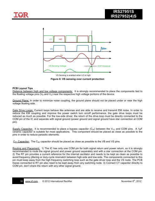
LO<br />
HO<br />
VS<br />
ILr<br />
VS Sensing Voltage<br />
OCP threshold<br />
VS Sensing is enabled when LO is high<br />
Figure 6: VS sensing over current protection<br />
PCB Layout Tips<br />
Distance between high and low voltage components: It is strongly recommended to place the components tied to<br />
the floating voltage pins (V B and V S ) near the respective high voltage portions of the device.<br />
Ground Plane: In order to minimize noise coupling, the ground plane should not be placed under or near the high<br />
voltage floating side.<br />
Gate Drive Loops: Current loops behave like antennas and are able to receive and transmit EM noise. In order to<br />
reduce the EM coupling and improve the power switch turn on/off performance, the gate drive loops must be<br />
reduced as much as possible. For the low-side driver, the return of the drive loop must be directly connected to the<br />
COM pin of the IC and separate with signal ground (power ground and signal ground have star connection at COM<br />
pin).<br />
Supply Capacitor: It is recommended to place a bypass capacitor (C IN ) between the V CC and COM pins. A 1μF<br />
ceramic capacitor is suitable for most applications. This component should be placed as close as possible to the<br />
pins in order to reduce parasitic elements.<br />
C BS Capacitor: The C BS capacitor should be placed as close as possible to the VB and VS pins.<br />
Routing and Placement: 1) The IC has only one COM pin for both signal return and power return, so it is strongly<br />
recommended to route the signal ground and power ground separately and with a star connection at the COM pin.<br />
2) The RT pin provides a current reference for the internal oscillator and needs to be kept as clean as possible to<br />
avoid frequency jittering or duty-cycle mismatch between high-side and low-side. The components connected to this<br />
pin must keep away from the high frequency switching loop such as the gate driver loop and the VS node. The PCB<br />
traces connected to RT pin also need to be kept away from any switching node. 3) Connect CT capacitor directly to<br />
COM pin, don’t share the return with any other signal ground.<br />
18 www.irf.com © 2012 <strong>International</strong> <strong>Rectifier</strong> November 8 th , 2012


