

IRS27951S IRS27952(4)S - International Rectifier
IRS27951S IRS27952(4)S - International Rectifier
IRS27951S IRS27952(4)S - International Rectifier

Create successful ePaper yourself
Turn your PDF publications into a flip-book with our unique Google optimized e-Paper software.
<strong>IRS27951S</strong><br />
<strong>IRS27952</strong>(4)S<br />
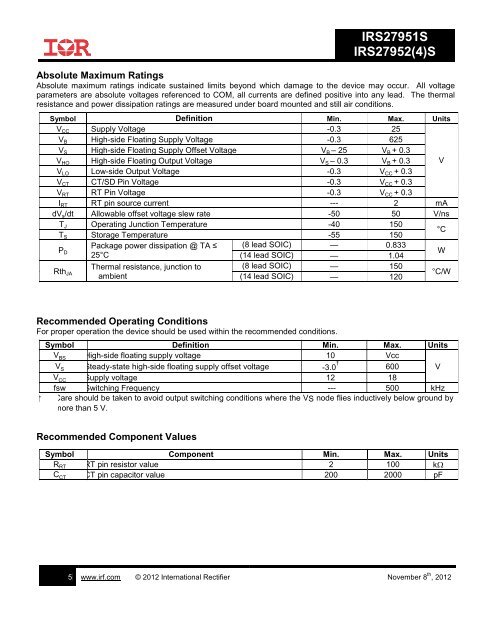
Absolute Maximum Ratings<br />
Absolute maximum ratings indicate sustained limits beyond which damage to the device may occur. All voltage<br />
parameters are absolute voltages referenced to COM, all currents are defined positive into any lead. The thermal<br />
resistance and power dissipation ratings are measured under board mounted and still air conditions.<br />
Symbol Definition Min. Max. Units<br />
V CC Supply Voltage -0.3 25<br />
V B High-side Floating Supply Voltage -0.3 625<br />
V S High-side Floating Supply Offset Voltage V B – 25 V B + 0.3<br />
V HO High-side Floating Output Voltage V S – 0.3 V B + 0.3 V<br />
V LO Low-side Output Voltage -0.3 V CC + 0.3<br />
V CT CT/SD Pin Voltage -0.3 V CC + 0.3<br />
V RT RT Pin Voltage -0.3 V CC + 0.3<br />
I RT RT pin source current --- 2 mA<br />
dV s /dt Allowable offset voltage slew rate -50 50 V/ns<br />
T J Operating Junction Temperature -40 150<br />
T S Storage Temperature -55 150<br />
°C<br />
P D<br />
Package power dissipation @ TA ≤ (8 lead SOIC) — 0.833<br />
25°C<br />
(14 lead SOIC) — 1.04<br />
W<br />
Rth JA<br />
Thermal resistance, junction to<br />
(8 lead SOIC) — 150<br />
ambient<br />
(14 lead SOIC) — 120<br />
°C/W<br />
Recommended Operating Conditions<br />
For proper operation the device should be used within the recommended conditions.<br />
Symbol Definition Min. Max. Units<br />
V BS High-side floating supply voltage 10 Vcc<br />
V S Steady-state high-side floating supply offset voltage -3.0 † 600 V<br />
V CC Supply voltage 12 18<br />
fsw Switching Frequency --- 500 kHz<br />
† Care should be taken to avoid output switching conditions where the VS node flies inductively below ground by<br />
more than 5 V.<br />
Recommended Component Values<br />
Symbol Component Min. Max. Units<br />
R RT RT pin resistor value 2 100 kΩ<br />
C CT CT pin capacitor value 200 2000 pF<br />
5 www.irf.com © 2012 <strong>International</strong> <strong>Rectifier</strong> November 8 th , 2012


