


You also want an ePaper? Increase the reach of your titles
YUMPU automatically turns print PDFs into web optimized ePapers that Google loves.
32-Channel, 3 V/5 V, Single-Supply,<br />
14-Bit denseDAC<br />
Data Sheet <strong>AD5382</strong><br />
FEATURES<br />
Guaranteed monotonic<br />
INL error: ±4 LSB max<br />
On-chip 1.25 V/2.5 V, 10 ppm/°C reference<br />
Temperature range: –40°C to +85°C<br />
Rail-to-rail output amplifier<br />
Power-down mode<br />
Package type: 100-lead LQFP (14 mm × 14 mm)<br />
User interfaces:<br />
Parallel<br />
Serial (SPI®-/QSPI-/MICROWIRE-/DSP-compatible,<br />
featuring data readback)<br />
I 2 C-compatible<br />
Robust 6.5 kV HBM and 2 kV FICDM ESD rating<br />
PD<br />
SER/PAR<br />
FIFO EN<br />
CS/(SYNC/AD0)<br />
WR/(DCEN/AD1)<br />
SDO<br />
DB13/(DIN/SDA)<br />
DB12/(SCLK/SCL)<br />
DB11/(SPI/I 2C)<br />
DB10<br />
DB0<br />
A4<br />
A0<br />
REG0<br />
REG1<br />
RESET<br />
BUSY<br />
CLR<br />
MON_IN1<br />
MON_IN2<br />
MON_IN3<br />
MON_IN4<br />
POWER-ON<br />
RESET<br />
Rev. C<br />
Information furnished by <strong>Analog</strong> <strong>Devices</strong> is believed to be accurate and reliable.<br />
However, no responsibility is assumed by <strong>Analog</strong> <strong>Devices</strong> for its use, nor for any<br />
infringements of patents or other rights of third parties that may result from its use.<br />
Specifications subject to change without notice. No license is granted by implication<br />
or otherwise under any patent or patent rights of <strong>Analog</strong> <strong>Devices</strong>. Trademarks and<br />
registered trademarks are the property of their respective owners.<br />
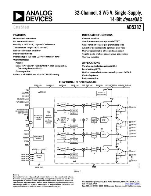
FUNCTIONAL BLOCK DIAGRAM<br />
14<br />
INPUT<br />
REG0<br />
14<br />
14<br />
14<br />
14<br />
m REG0<br />
c REG0<br />
14<br />
INPUT<br />
REG1<br />
14<br />
14<br />
14<br />
14<br />
m REG1<br />
c REG1<br />
14<br />
INPUT<br />
REG6<br />
14<br />
14<br />
14<br />
14<br />
m REG6<br />
c REG6<br />
INTEGRATED FUNCTIONS<br />
Channel monitor<br />
Simultaneous output update via LDAC<br />
Clear function to user-programmable code<br />
Amplifier boost mode to optimize slew rate<br />
User-programmable offset and gain adjust<br />
Toggle mode enables square wave generation<br />
Thermal monitor<br />
APPLICATIONS<br />
Variable optical attenuators (VOAs)<br />
Level setting (ATE)<br />
Optical micro-electro-mechanical systems (MEMS)<br />
Control systems<br />
Instrumentation<br />
DVDD (×3) DGND (×3) AVDD (×4) AGND (×4) DAC_GND (×4) REFGND REFOUT/REFIN SIGNAL_GND (×4)<br />
<strong>AD5382</strong><br />
INTERFACE<br />
CONTROL<br />
LOGIC<br />
VOUT0………VOUT31<br />
36-TO-1<br />
MUX<br />
FIFO<br />
+<br />
STATE<br />
MACHINE<br />
+<br />
CONTROL<br />
LOGIC<br />
14<br />
INPUT<br />
REG7<br />
14<br />
14<br />
14<br />
m REG7<br />
14<br />
c REG7<br />
×4<br />
DAC<br />
REG0<br />
DAC<br />
REG1<br />
DAC<br />
REG6<br />
DAC<br />
REG7<br />
MON_OUT LDAC<br />
Figure 1.<br />
1.25V/2.5V<br />
REFERENCE<br />
14<br />
14<br />
14<br />
14<br />
DAC 0<br />
DAC 1<br />
DAC 6<br />
DAC 7<br />
VOUT0<br />
VOUT1<br />
VOUT2<br />
VOUT3<br />
VOUT4<br />
VOUT5<br />
VOUT6<br />
VOUT7<br />
VOUT8<br />
VOUT31<br />
One Technology Way, P.O. Box 9106, Norwood, MA 02062-9106, U.S.A.<br />
Tel: 781.329.4700 www.analog.com<br />
Fax: 781.461.3113© 2004–2012 <strong>Analog</strong> <strong>Devices</strong>, Inc. All rights reserved.<br />
R<br />
R<br />
R<br />
R<br />
R<br />
R<br />
R<br />
R<br />
03733-001
<strong>AD5382</strong> Data Sheet<br />
TABLE OF CONTENTS<br />
General Description ......................................................................... 3<br />
Specifications ..................................................................................... 4<br />
<strong>AD5382</strong>-5 Specifications ............................................................. 4<br />
<strong>AD5382</strong>-3 Specifications ............................................................. 6<br />
AC Characteristics ........................................................................ 7<br />
Timing Characteristics ..................................................................... 8<br />
SPI-, QSPI-, MICROWIRE-, or DSP-Compatible Serial<br />
Interface ......................................................................................... 8<br />
I 2 C Serial Interface ...................................................................... 10<br />
Parallel Interface ......................................................................... 11<br />
Absolute Maximum Ratings .......................................................... 13<br />
ESD Caution ................................................................................ 13<br />
Pin Configuration and Function Descriptions ........................... 14<br />
Terminology .................................................................................... 17<br />
Typical Performance Characteristics ........................................... 18<br />
Functional Description .................................................................. 21<br />
DAC Architecture—General ..................................................... 21<br />
Data Decoding ............................................................................ 21<br />
On-Chip Special Function Registers (SFR) ............................ 22<br />
SFR Commands .......................................................................... 22<br />
Hardware Functions ....................................................................... 25<br />
Reset Function ............................................................................ 25<br />
REVISION HISTORY<br />
10/12—Rev. B to Rev. C<br />
Changes to Title and Features Section ........................................... 1<br />
Changes to General Description and Table 1 ............................... 3<br />
Deleted Table 2; Renumbered Sequentially................................... 3<br />
Changes to Table 2 ............................................................................ 4<br />
Changes to Table 3 ............................................................................ 6<br />
Changes to Output Voltage Settling Time and Slew Rate<br />
Parameters, Table 4 ........................................................................... 7<br />
Changes to t14, t17, and t19 Parameters, Table 5 .............................. 8<br />
Change to t18 Parameter, Table 7 ................................................... 11<br />
Changes to Table 8 and ESD Caution Section ............................ 13<br />
Changes to Figure 10, Figure 11, and Figure 14; Deleted<br />
Figure 13; Renumbered Sequentially ........................................... 18<br />
Rev. C | Page 2 of 40<br />
Asynchronous Clear Function .................................................. 25<br />
BUSY and LDAC Functions...................................................... 25<br />
FIFO Operation in Parallel Mode ............................................ 25<br />
Power-On Reset .......................................................................... 25<br />
Power-Down ............................................................................... 25<br />
<strong>AD5382</strong> Interfaces .......................................................................... 26<br />
DSP-, SPI-, MICROWIRE-Compatible Serial Interfaces ..... 26<br />
I 2 C Serial Interface ..................................................................... 28<br />
Parallel Interface ......................................................................... 30<br />
Microprocessor Interfacing ....................................................... 31<br />
Application Information ................................................................ 33<br />
Power Supply Decoupling ......................................................... 33<br />
Typical Configuration Circuit .................................................. 33<br />
Monitor Function ....................................................................... 34<br />
Toggle Mode Function ............................................................... 34<br />
Thermal Monitor Function ....................................................... 35<br />
<strong>AD5382</strong> in a MEMS-Based Optical Switch ............................ 35<br />
Optical Attenuators .................................................................... 36<br />
Outline Dimensions ....................................................................... 37<br />
Ordering Guide .......................................................................... 37<br />
Changes to Figure 16, Figure 18, and Figure 19 ......................... 19<br />
Change to Table 13 ......................................................................... 22<br />
Updated Outline Dimensions ....................................................... 37<br />
4/10—Rev. A to Rev. B<br />
Changes to Table 18 ....................................................................... 24<br />
Changes to Ordering Guide .......................................................... 37<br />
3/05—Rev. 0 to Rev. A<br />
Changes to Specifications ................................................................. 4<br />
Changes to Figure 43 ...................................................................... 35<br />
5/04—Revision 0: Initial Version
Data Sheet <strong>AD5382</strong><br />
GENERAL DESCRIPTION<br />
The <strong>AD5382</strong> is a complete, single-supply, 32-channel, 14-bit<br />
denseDAC® available in a 100-lead LQFP package. All 32 channels<br />
have an on-chip output amplifier with rail-to-rail operation. The<br />
<strong>AD5382</strong> includes an internal software-selectable 1.25 V/2.5 V,<br />
10 ppm/°C reference, an on-chip channel monitor function that<br />
multiplexes the analog outputs to a common MON_OUT pin<br />
for external monitoring, and an output amplifier boost mode<br />
that allows optimization of the amplifier slew rate.<br />
The <strong>AD5382</strong> contains a double-buffered parallel interface,<br />
which features a 20 ns WR pulse width, an SPI-, QSPI-,<br />
MICROWIRE-, DSP-compatible serial interface with<br />
interface speeds in excess of 30 MHz and an I 2 C®-compatible<br />
Rev. C | Page 3 of 40<br />
interface that supports a 400 kHz data transfer rate.<br />
An input register followed by a DAC register provides double<br />
buffering, allowing the DAC outputs to be updated independently<br />
or simultaneously using the LDAC input.<br />
Each channel has a programmable gain and offset adjust<br />
register that allows the user to fully calibrate any DAC<br />
channel. Power consumption is typically 0.25 mA/channel<br />
when operating with boost mode disabled.<br />
Table 1. Other High Channel Count, Low Voltage, Single Supply DACs in Product Portfolio<br />
Model Resolution AVDD Range Output Channels Linearity Error (LSB) Package Description Package Option<br />
AD5380BSTZ-5 14 Bits 4.5 V to 5.5 V 40 ±4 100-Lead LQFP ST-100<br />
AD5380BSTZ-3 14 Bits 2.7 V to 3.6 V 40 ±4 100-Lead LQFP ST-100<br />
AD5381BSTZ-5 12 Bits 4.5 V to 5.5 V 40 ±1 100-Lead LQFP ST-100<br />
AD5381BSTZ-3 12 Bits 2.7 V to 3.6 V 40 ±1 100-Lead LQFP ST-100<br />
AD5383BSTZ-5 12 Bits 4.5 V to 5.5 V 32 ±1 100-Lead LQFP ST-100<br />
AD5383BSTZ-3 12 Bits 2.7 V to 3.6 V 32 ±1 100-Lead LQFP ST-100<br />
AD5390BSTZ-5 14 Bits 4.5 V to 5.5 V 16 ±3 52-Lead LQFP ST-52<br />
AD5390BCPZ-5 14 Bits 4.5 V to 5.5 V 16 ±3 64-Lead LFCSP CP-64<br />
AD5390BSTZ-3 14 Bits 2.7 V to 3.6 V 16 ±4 52-Lead LQFP ST-52<br />
AD5390BCPZ-3 14 Bits 2.7 V to 3.6 V 16 ±4 64-Lead LFCSP CP-64<br />
AD5391BSTZ-5 12 Bits 4.5 V to 5.5 V 16 ±1 52-Lead LQFP ST-52<br />
AD5391BCPZ-5 12 Bits 4.5 V to 5.5 V 16 ±1 64-Lead LFCSP CP-64<br />
AD5391BSTZ-3 12 Bits 2.7 V to 3.6 V 16 ±1 52-Lead LQFP ST-52<br />
AD5391BCPZ-3 12 Bits 2.7 V to 3.6 V 16 ±1 64-Lead LFCSP CP-64<br />
AD5392BSTZ-5 14 Bits 4.5 V to 5.5 V 8 ±3 52-Lead LQFP ST-52<br />
AD5392BCPZ-5 14 Bits 4.5 V to 5.5 V 8 ±3 64-Lead LFCSP CP-64<br />
AD5392BSTZ-3 14 Bits 2.7 V to 3.6 V 8 ±4 52-Lead LQFP ST-52<br />
AD5392BCPZ-3 14 Bits 2.7 V to 3.6 V 8 ±4 64-Lead LFCSP CP-64
<strong>AD5382</strong> Data Sheet<br />
SPECIFICATIONS<br />
<strong>AD5382</strong>-5 SPECIFICATIONS<br />
AVDD = 4.5 V to 5.5 V; DVDD = 2.7 V to 5.5 V, AGND = DGND = 0 V; External REFIN = 2.5 V; all specifications TMIN to TMAX,<br />
unless otherwise noted.<br />
Table 2.<br />
Parameter <strong>AD5382</strong>-51 ACCURACY<br />
Unit Test Conditions/Comments<br />
Resolution 14 Bits<br />
Relative Accuracy2 (INL) ±4 LSB max<br />
Differential Nonlinearity (DNL) –1/+2 LSB max Guaranteed monotonic over temperature<br />
Zero-Scale Error 4 mV max<br />
Offset Error ±4 mV max Measured at Code 32 in the linear region<br />
Offset Error TC ±5 µV/°C typ<br />
Gain Error ±0.05 % FSR max At 25°C<br />
±0.06 % FSR max TMIN to TMAX<br />
Gain Temperature Coefficient3 2 ppm FSR/°C typ<br />
DC Crosstalk3 REFERENCE INPUT/OUTPUT<br />
Reference Input<br />
1 LSB max<br />
3<br />
Reference Input Voltage 2.5 V ±1% for specified performance, AVDD = 2xREFIN + 50 mV<br />
DC Input Impedance 1 MΩ min Typically 100 MΩ<br />
Input Current ±1 µA max Typically ±30 nA<br />
Reference Range<br />
1 to<br />
AVDD/2<br />
V min/max<br />
Reference Output4 Enabled via CR10 in the <strong>AD5382</strong> control register;<br />
CR12 selects the reference voltage<br />
Output Voltage 2.495/2.505 V min/max At ambient; CR12 = 1; optimized for 2.5 V operation<br />
1.22/1.28 V min/max 1.25 V reference selected; CR12 = 0<br />
Reference TC ±10 ppm/°C max Temperature range: +25°C to +85°C<br />
±15 ppm/°C max Temperature range: –40°C to +85°C<br />
Output Impedance<br />
OUTPUT CHARACTERISTICS<br />
800 Ω typ<br />
3<br />
Output Voltage Range2 0/AVDD V min/max<br />
Short-Circuit Current 40 mA max<br />
Load Current<br />
Capacitive Load Stability<br />
±1 mA max<br />
RL = ∞ 200 pF max<br />
RL = 5 kΩ 1000 pF max<br />
DC Output Impedance<br />
MONITOR PIN<br />
0.6 Ω max<br />
Output Impedance 1 kΩ typ<br />
Three-State Leakage Current 100 nA typ<br />
LOGIC INPUTS (EXCEPT SDA/SCL) 3 DVDD = 2.7 V to 5.5 V<br />
VIH, Input High Voltage<br />
VIL, Input Low Voltage<br />
2 V min<br />
DVDD > 3.6 V 0.8 V max<br />
DVDD ≤ 3.6 V 0.6 V max<br />
Input Current ±1 µA max Total for all pins, TA = TMIN to TMAX<br />
Pin Capacitance 10 pF max<br />
Rev. C | Page 4 of 40
Data Sheet <strong>AD5382</strong><br />
Parameter <strong>AD5382</strong>-5 1 Unit Test Conditions/Comments<br />
LOGIC INPUTS (SDA, SCL ONLY) 3<br />
VIH, Input High Voltage 0.7 × DVDD V min SMBus-compatible at DVDD < 3.6 V<br />
VIL, Input Low Voltage 0.3 × DVDD V max SMBus-compatible at DVDD < 3.6 V<br />
IIN, Input Leakage Current ±1 µA max<br />
VHYST, Input Hysteresis 0.05 × DVDD V min<br />
CIN, Input Capacitance 8 pF typ<br />
Glitch Rejection 50 ns max Input filtering suppresses noise spikes of less than 50 ns<br />
LOGIC OUTPUTS (BUSY, SDO) 3<br />
VOL, Output Low Voltage 0.4 V max DVDD = 5 V ± 10%, sinking 200 µA<br />
VOH, Output High Voltage DVDD – 1 V min DVDD = 5 V ± 10%, sourcing 200 µA<br />
VOL, Output Low Voltage 0.4 V max DVDD = 2.7 V to 3.6 V, sinking 200 µA<br />
VOH, Output High Voltage DVDD – 0.5 V min DVDD = 2.7 V to 3.6 V, sourcing 200 µA<br />
High Impedance Leakage Current ±1 µA max SDO only<br />
High Impedance Output Capacitance 5 pF typ SDO only<br />
LOGIC OUTPUT (SDA) 3<br />
VOL, Output Low Voltage 0.4 V max ISINK = 3 mA<br />
0.6 V max ISINK = 6 mA<br />
Three-State Leakage Current ±1 µA max<br />
Three-State Output Capacitance 8 pF typ<br />
POWER REQUIREMENTS<br />
AVDD 4.5/5.5 V min/max<br />
DVDD 2.7/5.5 V min/max<br />
Power Supply Sensitivity 3<br />
∆Midscale/∆ΑVDD –85 dB typ<br />
AIDD 0.375 mA/channel max Outputs unloaded, boost off. 0.25 mA/channel typ<br />
0.475 mA/channel max Outputs unloaded, boost on. 0.325 mA/channel typ<br />
DIDD 1 mA max VIH = DVDD, VIL = DGND.<br />
AIDD (Power-Down) 20 µA max Typically 100 nA<br />
DIDD (Power-Down) 20 µA max Typically 1 µA<br />
Power Dissipation 65 mW max Outputs unloaded, boost off, AVDD = DVDD = 5 V<br />
1 <strong>AD5382</strong>-5 is calibrated using an external 2.5 V reference. Temperature range for all versions: –40°C to +85°C.<br />
2 Accuracy guaranteed from VOUT = 10 mV to AVDD – 50 mV.<br />
3 Guaranteed by characterization, not production tested.<br />
4 Default on the <strong>AD5382</strong>-5 is 2.5 V. Programmable to 1.25 V via CR12 in the <strong>AD5382</strong> control register; operating the <strong>AD5382</strong>-5 with a 1.25 V reference leads to degraded<br />
accuracy specifications.<br />
Rev. C | Page 5 of 40
<strong>AD5382</strong> Data Sheet<br />
<strong>AD5382</strong>-3 SPECIFICATIONS<br />
AVDD = 2.7 V to 3.6 V; DVDD = 2.7 V to 5.5 V, AGND = DGND = 0 V; external REFIN = 1.25 V; all specifications TMIN to TMAX,<br />
unless otherwise noted.<br />
Table 3.<br />
Parameter <strong>AD5382</strong>-3 1 ACCURACY<br />
Unit Test Conditions/Comments<br />
Resolution 14 Bits<br />
Relative Accuracy2 (INL) ±4 LSB max<br />
Differential Nonlinearity (DNL) –1/+2 LSB max Guaranteed monotonic over temperature<br />
Zero-Scale Error 4 mV max<br />
Offset Error ±4 mV max Measured at Code 64 in the linear region<br />
Offset Error TC ±5 µV/°C typ<br />
Gain Error ±0.05 % FSR max At 25°C<br />
±0.1 % FSR max TMIN to TMAX<br />
Gain Temperature Coefficient 3 2 ppm FSR/°C typ<br />
DC Crosstalk3 REFERENCE INPUT/OUTPUT<br />
Reference Input<br />
1 LSB max<br />
3<br />
Reference Input Voltage 1.25 V ±1% for specified performance<br />
DC Input Impedance 1 MΩ min Typically 100 MΩ<br />
Input Current ±10 µA max Typically ±30 nA<br />
Reference Range 1 to AVDD/2 V min/max<br />
Reference Output4 Enabled via CR10 in the <strong>AD5382</strong> control register,<br />
CR12 selects the reference voltage<br />
Output Voltage 1.245/1.255 V min/max At ambient; CR12 = 0; optimized for 1.25 V operation<br />
2.47/2.53 V min/max 2.5 V reference selected; CR12 = 1<br />
Reference TC ±10 ppm/°C max Temperature Range: +25°C to +85°C<br />
±15 ppm/°C max Temperature Range: –40°C to +85°C<br />
Output Impedance<br />
OUTPUT CHARACTERISTICS<br />
800 Ω typ<br />
3<br />
Output Voltage Range2 0/AVDD V min/max<br />
Short-Circuit Current 40 mA max<br />
Load Current<br />
Capacitive Load Stability<br />
±1 mA max<br />
RL = ∞ 200 pF max<br />
RL = 5 kΩ 1000 pF max<br />
DC Output Impedance<br />
MONITOR PIN (MON OUT)<br />
0.6 Ω max<br />
Output Impedance 1 kΩ typ<br />
Three-State Leakage Current 100 nA typ<br />
LOGIC INPUTS (EXCEPT SDA/SCL) 3 DVDD = 2.7 V to 3.6 V<br />
VIH, Input High Voltage<br />
VIL, Input Low Voltage<br />
2 V min<br />
DVDD > 3.6 V 0.8 V max<br />
DVDD ≤ 3.6 V 0.6 V max<br />
Input Current ±1 µA max Total for all pins, TA = TMIN to TMAX<br />
Pin Capacitance<br />
LOGIC INPUTS (SDA, SCL ONLY)<br />
10 pF max<br />
3<br />
VIH, Input High Voltage 0.7 × DVDD V min SMBus-compatible at DVDD < 3.6 V<br />
VIL, Input Low Voltage 0.3 × DVDD V max SMBus-compatible at DVDD < 3.6 V<br />
IIN, Input Leakage Current ±1 µAmax<br />
VHYST, Input Hysteresis 0.05 × DVDD V min<br />
CIN, Input Capacitance 8 pF typ<br />
Glitch Rejection 50 ns max Input filtering suppresses noise spikes of less than 50 ns<br />
Rev. C | Page 6 of 40
Data Sheet <strong>AD5382</strong><br />
Parameter <strong>AD5382</strong>-3 1 Unit Test Conditions/Comments<br />
LOGIC OUTPUTS (BUSY, SDO) 3<br />
VOL, Output Low Voltage 0.4 V max Sinking 200 µA<br />
VOH, Output High Voltage DVDD – 0.5 V min Sourcing 200 µA<br />
High Impedance Leakage Current ±1 µA max SDO only<br />
High Impedance Output Capacitance 5 pF typ SDO only<br />
LOGIC OUTPUT (SDA) 3<br />
VOL, Output Low Voltage 0.4 V max ISINK = 3 mA<br />
0.6 V max ISINK = 6 mA<br />
Three-State Leakage Current ±1 µA max<br />
Three-State Output Capacitance 8 pF typ<br />
POWER REQUIREMENTS<br />
AVDD 2.7/3.6 V min/max<br />
DVDD 2.7/5.5 V min/max<br />
Power Supply Sensitivity 3<br />
∆Midscale/∆ΑVDD –85 dB typ<br />
AIDD 0.375 mA/channel max Outputs unloaded; boost off; 0.25 mA/channel typ<br />
0.475 mA/channel max Outputs unloaded; boost on; 0.325 mA/channel typ<br />
DIDD 1 mA max VIH = DVDD VIL = DGND<br />
AIDD (Power-Down) 20 µA max Typically 100 nA<br />
DIDD (Power-Down) 20 µA max Typically 1 µA<br />
Power Dissipation 39 mW max Outputs unloaded; boost off; AVDD = DVDD = 3 V<br />
1 <strong>AD5382</strong>-3 is calibrated using an external 1.25 V reference. Temperature range is –40°C to +85°C.<br />
2 Accuracy guaranteed from VOUT = 10 mV to AVDD – 50 mV.<br />
3 Guaranteed by characterization, not production tested.<br />
4 Default on the <strong>AD5382</strong>-5 is 2.5 V. Programmable to 1.25 V via CR12 in the <strong>AD5382</strong> control register; operating the <strong>AD5382</strong>-5 with a 1.25 V reference leads to degraded<br />
accuracy specifications.<br />
AC CHARACTERISTICS 1<br />
AVDD = 4.5 V to 5.5 V or 2.7 V to 3.6 V; DVDD = 2.7 V to 5.5 V; AGND = DGND= 0 V.<br />
Table 4.<br />
Parameter All Unit Test Conditions/Comments<br />
DYNAMIC PERFORMANCE<br />
Output Voltage Settling Time 2 1/4 scale to 3/4 scale change settling to ±1 LSB<br />
3 µs typ<br />
8 µs max<br />
Slew Rate 2 1.5 V/µs typ Boost mode off, CR11 = 0<br />
2.5 V/µs typ Boost mode on, CR11 = 1<br />
Digital-to-<strong>Analog</strong> Glitch Energy 12 nV-s typ<br />
Glitch Impulse Peak Amplitude 15 mV typ<br />
DAC-to-DAC Crosstalk 1 nV-s typ See Terminology section<br />
Digital Crosstalk 0.8 nV-s typ<br />
Digital Feedthrough 0.1 nV-s typ Effect of input bus activity on DAC output under test<br />
Output Noise 0.1 Hz to 10 Hz 15 µV p-p typ External reference, midscale loaded to DAC<br />
40 µV p-p typ Internal reference, midscale loaded to DAC<br />
Output Noise Spectral Density<br />
at 1 kHz 150 nV/√Hz typ<br />
at 10 kHz 100 nV/√Hz typ<br />
1 Guaranteed by design and characterization, not production tested.<br />
2 The slew rate can be programmed via the current boost control bit (CR11) in the <strong>AD5382</strong> control register.<br />
Rev. C | Page 7 of 40
<strong>AD5382</strong> Data Sheet<br />
TIMING CHARACTERISTICS<br />
SPI-, QSPI-, MICROWIRE-, OR DSP-COMPATIBLE SERIAL INTERFACE<br />
DVDD = 2.7 V to 5.5 V; AVDD = 4.5 V to 5.5 V or 2.7 V to 3.6 V; AGND = DGND = 0 V; all specifications TMIN to TMAX,<br />
unless otherwise noted.<br />
Table 5.<br />
Parameter 1, 2, 3 Limit at TMIN, TMAX Unit Description<br />
t1 33 ns min SCLK cycle time<br />
t2 13 ns min SCLK high time<br />
t3 13 ns min SCLK low time<br />
t4 13 ns min SYNC falling edge to SCLK falling edge setup time<br />
t5 4 13 ns min 24th SCLK falling edge to SYNC falling edge<br />
t6 4 33 ns min Minimum SYNC low time<br />
t7 10 ns min Minimum SYNC high time<br />
t7A 50 ns min Minimum SYNC high time in readback mode<br />
t8 5 ns min Data setup time<br />
t9 4.5 ns min Data hold time<br />
t10 4 30 ns max 24th SCLK falling edge to BUSY falling edge<br />
t11 670 ns max BUSY pulse width low (single channel update)<br />
t12 4 20 ns min 24th SCLK falling edge to LDAC falling edge<br />
t13 20 ns min LDAC pulse width low<br />
t14 2 µs max BUSY rising edge to DAC output response time<br />
t15 0 ns min BUSY rising edge to LDAC falling edge<br />
t16 100 ns min LDAC falling edge to DAC output response time<br />
t17 2 µs typ DAC output settling time<br />
t18 20 ns min CLR pulse width low<br />
t19 40 µs max CLR pulse activation time<br />
t20 5 20 ns max SCLK rising edge to SDO valid<br />
t21 5 5 ns min SCLK falling edge to SYNC rising edge<br />
t22 5 8 ns min SYNC rising edge to SCLK rising edge<br />
t23 20 ns min SYNC rising edge to LDAC falling edge<br />
1 Guaranteed by design and characterization, not production tested.<br />
2 All input signals are specified with tr = tf = 5 ns (10% to 90% of VCC) and are timed from a voltage level of 1.2 V.<br />
3 See Figure 2, Figure 3, Figure 4, and Figure 5.<br />
4 Standalone mode only.<br />
5 Daisy-chain mode only.<br />
TO OUTPUT PIN<br />
C L<br />
50pF<br />
200µA<br />
200µA<br />
I OL<br />
I OH<br />
Rev. C | Page 8 of 40<br />
V OH (MIN) OR<br />
V OL (MAX)<br />
Figure 2. Load Circuit for SDO Timing Diagram<br />
(Serial Interface, Daisy-Chain Mode)<br />
03733-002
Data Sheet <strong>AD5382</strong><br />
SCLK<br />
SYNC<br />
DIN<br />
SDO<br />
SCLK<br />
SYNC<br />
DIN<br />
SDO<br />
LDAC<br />
SCLK<br />
SYNC<br />
DIN<br />
BUSY<br />
LDAC 1<br />
VOUT1<br />
LDAC 2<br />
VOUT2<br />
t 7<br />
CLR<br />
VOUT<br />
t 4<br />
t 3<br />
t 7 t8 t 9<br />
DB23<br />
t 6<br />
t 18<br />
1LDAC ACTIVE DURING BUSY<br />
2 LDAC ACTIVE AFTER BUSY<br />
t 1<br />
t 19<br />
24<br />
t 2 t5<br />
DB0<br />
Figure 3. Serial Interface Timing Diagram (Standalone Mode)<br />
t 7A<br />
t 12<br />
t 10<br />
Rev. C | Page 9 of 40<br />
t 11<br />
24 48<br />
DB23 DB0 DB23 DB0<br />
t 4<br />
INPUT WORD SPECIFIES<br />
REGISTER TO BE READ<br />
t 8 t 9<br />
UNDEFINED<br />
t 13<br />
t 15<br />
t 14<br />
t 16<br />
NOP CONDITION<br />
24<br />
t 17<br />
t 13<br />
t 17<br />
DB23 DB0<br />
Figure 4. Serial Interface Timing Diagram (Data Readback Mode)<br />
t 3<br />
t 1<br />
t 2<br />
24<br />
t 20<br />
SELECTED REGISTER<br />
DATA CLOCKED OUT 03733-004<br />
DB23 DB0 DB23<br />
DB0<br />
INPUT WORD FOR DAC N INPUT WORD FOR DAC N + 1<br />
t 21<br />
48<br />
DB23 DB0<br />
UNDEFINED INPUT WORD FOR DAC N<br />
Figure 5. Serial Interface Timing Diagram (Daisy-Chain Mode)<br />
t 22<br />
t 23<br />
03733-003<br />
t 13<br />
03733-005
<strong>AD5382</strong> Data Sheet<br />
I 2 C SERIAL INTERFACE<br />
DVDD = 2.7 V to 5.5 V; AVDD = 4.5 V to 5.5 V or 2.7 V to 3.6 V; AGND = DGND = 0 V; all specifications TMIN to TMAX,<br />
unless otherwise noted.<br />
Table 6.<br />
Parameter1, 2 Limit at TMIN, TMAX Unit Description<br />
FSCL 400 kHz max SCL clock frequency<br />
t1 2.5 µs min SCL cycle time<br />
t2 0.6 µs min tHIGH, SCL high time<br />
t3 1.3 µs min tLOW, SCL low time<br />
t4 0.6 µs min tHD,STA, start/repeated start condition hold time<br />
t5 100 ns min tSU,DAT, data setup time<br />
t6 3 0.9 µs max tHD,DAT, data hold time<br />
0 µs min tHD,DAT, data hold time<br />
t7 0.6 µs min tSU,STA, setup time for repeated start<br />
t8 0.6 µs min tSU,STO, stop condition setup time<br />
t9 1.3 µs min tBUF, bus free time between a stop and a start condition<br />
t10 300 ns max tR, rise time of SCL and SDA when receiving<br />
0 ns min tR, rise time of SCL and SDA when receiving (CMOS-compatible)<br />
t11 300 ns max tF, fall time of SDA when transmitting<br />
0 ns min tF, fall time of SDA when receiving (CMOS-compatible)<br />
300 ns max tF, fall time of SCL and SDA when receiving<br />
20 + 0.1Cb 4 ns min tF, fall time of SCL and SDA when transmitting<br />
Cb 400 pF max Capacitive load for each bus line<br />
1 Guaranteed by design and characterization, not production tested.<br />
2 See Figure 6.<br />
3 A master device must provide a hold time of at least 300 ns for the SDA signal (referred to the VIH min of the SCL signal) in order to bridge the undefined region of<br />
SCL’s falling edge.<br />
4<br />
Cb is the total capacitance, in pF, of one bus line. tR and tF are measured between 0.3 DVDD and 0.7 DVDD.<br />
SDA<br />
SCL<br />
t 9<br />
t 4<br />
START<br />
CONDITION<br />
t 3<br />
t 10<br />
t 6<br />
t 2<br />
t 11<br />
t 5<br />
Rev. C | Page 10 of 40<br />
t 7<br />
t 4<br />
REPEATED<br />
START<br />
CONDITION<br />
Figure 6. I 2 C-Compatible Serial Interface Timing Diagram<br />
t 1<br />
t 8<br />
STOP<br />
CONDITION<br />
03733-006
Data Sheet <strong>AD5382</strong><br />
PARALLEL INTERFACE<br />
DVDD = 2.7 V to 5.5 V; AVDD = 4.5 V to 5.5 V or 2.7 V to 3.6 V; AGND = DGND = 0 V; all specifications Tmin to Tmax,<br />
unless otherwise noted.<br />
Table 7.<br />
Parameter 1, 2, 3 Limit at TMIN, TMAX Unit Description<br />
t0 4.5 ns min REG0, REG1, address to WR rising edge setup time<br />
t1 4.5 ns min REG0, REG1, address to WR rising edge hold time<br />
t2 20 ns min CS pulse width low<br />
t3 20 ns min WR pulse width low<br />
t4 0 ns min CS to WR falling edge setup time<br />
t5 0 ns min WR to CS rising edge hold time<br />
t6 4.5 ns min Data to WR rising edge setup time<br />
t7 4.5 ns min Data to WR rising edge hold time<br />
t8 20 ns min WR pulse width high<br />
t9 4 700 ns min Minimum WR cycle time (single-channel write)<br />
t10 4 30 ns max WR rising edge to BUSY falling edge<br />
t11 4, 5 670 ns max BUSY pulse width low (single-channel update)<br />
t12 30 ns min WR rising edge to LDAC falling edge<br />
t13 20 ns min LDAC pulse width low<br />
t14 100 ns max BUSY rising edge to DAC output response time<br />
t15 20 ns min LDAC rising edge to WR rising edge<br />
t16 0 ns min BUSY rising edge to LDAC falling edge<br />
t17 100 ns min LDAC falling edge to DAC output response time<br />
t18 2 µs typ DAC output settling time<br />
t19 20 ns min CLR pulse width low<br />
t20 35 µsmax CLR pulse activation time<br />
1 Guaranteed by design and characterization, not production tested.<br />
2 All input signals are specified with tR = tR = 5 ns (10% to 90% of DVDD) and timed from a voltage level of 1.2 V.<br />
3 See Figure 7.<br />
4 See Figure 28.<br />
5 Measured with the load circuit of Figure 2.<br />
Rev. C | Page 11 of 40
<strong>AD5382</strong> Data Sheet<br />
REG0, REG1, A4...A0<br />
CS<br />
WR<br />
DB13...DB0<br />
BUSY<br />
LDAC 1<br />
VOUT1<br />
LDAC 2<br />
VOUT2<br />
CLR<br />
VOUT<br />
t 4<br />
t 2<br />
t 3<br />
t 0<br />
t 6<br />
t 5<br />
t 10<br />
t 19<br />
t 1<br />
t7<br />
t 12<br />
t 8<br />
t 20<br />
1LDAC ACTIVE DURING BUSY<br />
2LDAC ACTIVE AFTER BUSY 03733-007<br />
Rev. C | Page 12 of 40<br />
t 11<br />
t 9<br />
t 13<br />
Figure 7. Parallel Interface Timing Diagram<br />
t 15<br />
t 14<br />
t 16<br />
t 17<br />
t 18<br />
t 13<br />
t 18
Data Sheet <strong>AD5382</strong><br />
ABSOLUTE MAXIMUM RATINGS<br />
TA = 25°C, unless otherwise noted 1 .<br />
Table 8.<br />
Parameter Rating<br />
AVDD to AGND –0.3 V to +7 V<br />
DVDD to DGND –0.3 V to +7 V<br />
Digital Inputs to DGND –0.3 V to DVDD + 0.3 V<br />
SDA/SCL to DGND –0.3 V to + 7 V<br />
Digital Outputs to DGND –0.3 V to DVDD + 0.3 V<br />
REFIN/REFOUT to AGND –0.3 V to AVDD + 0.3 V<br />
AGND to DGND –0.3 V to +0.3 V<br />
VOUTx to AGND –0.3 V to AVDD+ 0.3 V<br />
<strong>Analog</strong> Inputs to AGND –0.3 V to AVDD + 0.3 V<br />
MON_IN Inputs to AGND –0.3 V to AVDD + 0.3 V<br />
MON_OUT to AGND –0.3 V to AVDD + 0.3 V<br />
Operating Temperature Range<br />
Commercial (B Version) –40°C to +85°C<br />
Storage Temperature Range –65°C to +150°C<br />
JunctionTemperature (TJ max) 150°C<br />
100-lead LQFP Package<br />
θJAThermal Impedance 44°C/W<br />
Reflow Soldering<br />
Peak Temperature 230°C<br />
ESD<br />
HBM 6.5 kV<br />
FICDM 2 kV<br />
1 Transient currents of up to 100 mA do not cause SCR latch-up.<br />
Rev. C | Page 13 of 40<br />
Stresses above those listed under Absolute Maximum Ratings<br />
may cause permanent damage to the device. This is a stress<br />
rating only; functional operation of the device at these or any<br />
other conditions above those listed in the operational sections<br />
of this specification is not implied. Exposure to absolute<br />
maximum rating conditions for extended periods may affect<br />
device reliability.<br />
ESD CAUTION
<strong>AD5382</strong> Data Sheet<br />
PIN CONFIGURATION AND FUNCTION DESCRIPTIONS<br />
FIFO EN<br />
CLR<br />
VOUT24<br />
VOUT25<br />
VOUT26<br />
VOUT27<br />
SIGNAL_GND4<br />
DAC_GND4<br />
AGND4<br />
AVDD4<br />
VOUT28<br />
VOUT29<br />
VOUT30<br />
VOUT31<br />
REFGND<br />
REFOUT/REFIN<br />
SIGNAL_GND1<br />
DAC_GND1<br />
AVDD1<br />
VOUT0<br />
VOUT1<br />
VOUT2<br />
VOUT3<br />
VOUT4<br />
AGND1<br />
1<br />
2<br />
3<br />
4<br />
5<br />
6<br />
7<br />
8<br />
9<br />
10<br />
11<br />
12<br />
13<br />
14<br />
15<br />
16<br />
17<br />
18<br />
19<br />
20<br />
21<br />
22<br />
23<br />
24<br />
25<br />
CS/(SYNC/AD0)<br />
DB13/(DIN/SDA)<br />
DB12/(SCLK/SCL)<br />
DB11/(SPI/I2C) DB10<br />
DB9<br />
DB8<br />
SDO(A/B)<br />
DVDD<br />
DGND<br />
DGND<br />
NC<br />
A4<br />
A3<br />
A2<br />
A1<br />
A0<br />
DVDD<br />
DVDD<br />
DGND<br />
SER/PAR<br />
PD<br />
WR (DCEN/AD1)<br />
LDAC<br />
BUSY<br />
100<br />
99<br />
98<br />
97<br />
96<br />
95<br />
94<br />
93<br />
92<br />
91<br />
90<br />
89<br />
88<br />
87<br />
86<br />
85<br />
84<br />
83<br />
82<br />
81<br />
80<br />
79<br />
78<br />
77<br />
76<br />
PIN 1<br />
IDENTIFIER<br />
<strong>AD5382</strong><br />
TOP VIEW<br />
(Not to Scale)<br />
26<br />
27<br />
28<br />
29<br />
30<br />
31<br />
32<br />
33<br />
34<br />
35<br />
36<br />
37<br />
38<br />
39<br />
40<br />
41<br />
42<br />
43<br />
44<br />
45<br />
46<br />
47<br />
48<br />
49<br />
50<br />
NC<br />
NC<br />
NC<br />
NC<br />
VOUT5<br />
VOUT6<br />
VOUT7<br />
NC<br />
NC<br />
MON_IN1<br />
MON_IN2<br />
MON_IN3<br />
MON_IN4<br />
NC<br />
MON_OUT<br />
VOUT8<br />
VOUT9<br />
VOUT10<br />
VOUT11<br />
VOUT12<br />
DAC_GND2<br />
SIGNAL_GND2<br />
VOUT13<br />
VOUT14<br />
VOUT15<br />
Figure 8. 100-Lead LQFP Pin Configuration<br />
Rev. C | Page 14 of 40<br />
75<br />
74<br />
73<br />
72<br />
71<br />
70<br />
69<br />
68<br />
67<br />
66<br />
65<br />
64<br />
63<br />
62<br />
61<br />
60<br />
59<br />
58<br />
57<br />
56<br />
55<br />
54<br />
53<br />
52<br />
51<br />
RESET<br />
DB7<br />
DB6<br />
DB5<br />
DB4<br />
DB3<br />
DB2<br />
DB1<br />
DB0<br />
REG0<br />
REG1<br />
VOUT23<br />
VOUT22<br />
VOUT21<br />
VOUT20<br />
AVDD3<br />
AGND3<br />
DAC_GND3<br />
SIGNAL_GND3<br />
VOUT19<br />
VOUT18<br />
VOUT17<br />
VOUT16<br />
AVDD2<br />
AGND2<br />
Table 9. Pin Function Descriptions<br />
Mnemonic Function<br />
VOUTx Buffered <strong>Analog</strong> Outputs for Channel x. Each analog output is driven by a rail-to-rail output amplifier operating at a<br />
gain of 2. Each output is capable of driving an output load of 5 kΩ to ground. Typical output impedance is 0.5 Ω.<br />
SIGNAL_GND(1–4) <strong>Analog</strong> Ground Reference Points for Each Group of Eight Output Channels. All SIGNAL_GND pins are tied together<br />
internally and should be connected to the AGND plane as close as possible to the <strong>AD5382</strong>.<br />
DAC_GND(1–4) Ground Reference point for the Internal 14-Bit DAC. Each group of eight channels contains a DAC_GND pin. These<br />
pins shound be connected to the AGND plane.<br />
AGND(1–4) <strong>Analog</strong> Ground Reference Point. Each group of eight channels contains an AGND pin. All AGND pins should be<br />
connected externally to the AGND plane.<br />
AVDD(1–4) <strong>Analog</strong> Supply Pins. Each group of eight channels has a separate AVDD pin. These pins are internally shorted and<br />
should be decoupled with a 0.1 µF ceramic capacitor and a 10 µF tantalum capacitor. Operating range for the<br />
<strong>AD5382</strong>-5 is 4.5 V to 5.5 V; operating range for the <strong>AD5382</strong>-3 is 2.7 V to 3.6 V.<br />
DGND Ground for All Digital Circuitry.<br />
DVDD Logic Power Supply. Guaranteed operating range is 2.7 V to 5.5 V. It is recommended that these pins be decoupled<br />
with 0.1 µF ceramic and 10 µF tantalum capacitors to DGND.<br />
REFGND Ground Reference Point for the Internal Reference.<br />
REFOUT/REFIN Reference Output when the Internal Reference is Selected. The <strong>AD5382</strong> contains a common REFOUT/REFIN pin. If the<br />
application requires an external reference, it can be applied to this pin, and the internal reference can be disabled<br />
via the control register. The default for this pin is a reference input.<br />
03733-008
Data Sheet <strong>AD5382</strong><br />
Mnemonic Function<br />
MON_OUT Monitor Output. When the monitor function is enabled, this pin acts as the output of a 36-to-1 channel multiplexer<br />
that can be programmed to multiplex one of Channels 0 to 31 or any of the monitor input pins (MON_IN1 to<br />
MON_IN4) to the MON_OUT pin. The MON_OUT pin’s output impedance is typically 500 Ω and is intended to drive a<br />
high input impedance like that exhibited by SAR ADC inputs.<br />
MON_INx Monitor Input Pins. The <strong>AD5382</strong> contains four monitor input pins that allow the user to connect input signals, within<br />
the maximum ratings of the device, to these pins for monitoring purposes. Any of the signals applied to the MON_IN<br />
pins, along with the 32 output channels, can be switched to the MON_OUT pin via software. For example, an<br />
external ADC can be used to monitor these signals.<br />
SER/PAR Interface Select Input. This pin allows the user to select whether the serial or parallel interface is used. If it is tied<br />
high, the serial interface mode is selected and Pin 97 (SPI/I 2 C) is used to determine if the interface mode is SPI or I 2 C.<br />
Parallel interface mode is selected when SER/PAR is low.<br />
CS/(SYNC/AD0) In parallel interface mode, this pin acts as the chip select input (level sensitive, active low). When low, the <strong>AD5382</strong> is<br />
selected.<br />
In serial interface mode, this is the frame synchronization input signal for the serial clocks before the addressed<br />
register is updated.<br />
In I2C mode, this pin acts as a hardware address pin used in conjunction with AD1 to determine the software address<br />
for the device on the I2C bus.<br />
WR/(DCEN/AD1) Multifunction Pin. In parallel interface mode, this pin acts as write enable. In serial interface mode, this pin acts as a<br />
daisy-chain enable in SPI mode and as a hardware address pin in I2C mode.<br />
Parallel Interface Write Input (Edge Sensitive). The rising edge of WR is used in conjunction with CS low, and the<br />
address bus inputs to write to the selected device registers.<br />
Serial Interface. Daisy-chain select input (level sensitive, active high). When high, this signal is used in conjunction<br />
with SER/PAR high to enable the SPI serial interface daisy-chain mode.<br />
I2C Mode. This pin acts as a hardware address pin used in conjunction with AD0 to determine the software address<br />
for this device on the I2C bus.<br />
DB13–DB0 Parallel Data Bus. DB13 is the MSB and DB0 is the LSB of the input data-word on the <strong>AD5382</strong>.<br />
A4–A0 Parallel Address Inputs. A4 to A0 are decoded to address one of the <strong>AD5382</strong>’s 40 input channels. Used in conjunction<br />
with the REG1 and REG0 pins to determine the destination register for the input data.<br />
REG1, REG0 In parallel interface mode, REG1 and REG0 are used in decoding the destination registers for the input data. REG1<br />
and REG0 are decoded to address the input data register, offset register, or gain register for the selected channel and<br />
are also used to decide the special function registers.<br />
SDO/(A/B) Serial Data Output in Serial Interface Mode. Three-stateable CMOS output. SDO can be used for daisy-chaining a<br />
number of devices together. Data is clocked out on SDO on the rising edge of SCLK, and is valid on the falling edge<br />
of SCLK.<br />
In parallel interface mode, this pin acts as the A or B data register select when writing data to the <strong>AD5382</strong>’s data<br />
registers with toggle mode selected (see the Toggle Mode Function section). In toggle mode, the LDAC is used to<br />
switch the output between the data contained in the A and B data registers. All DAC channels contain two data<br />
registers. In normal mode, Data Register A is the default for data transfers.<br />
BUSY Digital CMOS Output. BUSY goes low during internal calculations of the data (x2) loaded to the DAC data register.<br />
During this time, the user can continue writing new data to the x1, c, and m registers, but no further updates to the<br />
DAC registers and DAC outputs can take place. If LDAC is taken low while BUSY is low, this event is stored. BUSY also<br />
goes low during power-on reset, and when the RESET pin is low. During this time, the interface is disabled and any<br />
events on LDAC are ignored. A CLR operation also brings BUSY low.<br />
LDAC Load DAC Logic Input (Active Low). If LDAC is taken low while BUSY is inactive (high), the contents of the input<br />
registers are transferred to the DAC registers, and the DAC outputs are updated. If LDAC is taken low while BUSY is<br />
active and internal calculations are taking place, the LDAC event is stored and the DAC registers are updated when<br />
BUSY goes inactive. However, any events on LDAC during power-on reset or on RESET are ignored.<br />
CLR<br />
Asynchronous Clear Input. The CLR input is falling edge sensitive. When CLR is activated, all channels are updated<br />
with the data in the CLR code register. BUSY is low for 35 µs while all channels are being updated with the CLR code.<br />
RESET Asynchronous Digital Reset Input (Falling Edge Sensitive). The function of this pin is equivalent to that of the poweron<br />
reset generator. When this pin is taken low, the state machine initiates a reset sequence to digitally reset the x1,<br />
m, c, and x2 registers to their default power-on values. This sequence takes 270 µs. The falling edge of RESET initiates<br />
the RESET process and BUSY goes low for the duration, returning high when RESET is complete. While BUSY is low,<br />
all interfaces are disabled and all LDAC pulses are ignored. When BUSY returns high, the part resumes normal<br />
operation, and the status of the RESET pin is ignored until the next falling edge is detected.<br />
Rev. C | Page 15 of 40
<strong>AD5382</strong> Data Sheet<br />
Mnemonic Function<br />
PD Power Down (Level Sensitive, Active High). PD is used to place the device in to low power mode where the device<br />
consumes 2 µA AIDD and 20 µA DIDD. In power-down mode, all internal analog circuitry is placed in low power<br />
mode, and the analog output is configured as a high impedance output or provides a 100 kΩ load to ground,<br />
depending on how the power-down mode is configured. The serial interface remains active during power-down.<br />
FIFO EN FIFO Enable (Level Sensitive, Active High). When connected to DVDD, the internal FIFO is enabled, allowing the user<br />
to write to the device at full speed. FIFO is available only in parallel interface mode. The status of the FIFO EN pin is<br />
sampled on power-up, and also following a CLEAR or RESET, to determine if the FIFO is enabled. In either serial or I 2 C<br />
interface modes, the FIFO EN pin should be tied low.<br />
DB11/(SPI/I 2 C) Multifunction Input Pin. In parallel interface mode, this pin acts as DB11 of the parallel input data-word. In serial<br />
interface mode, this pin acts as serial interface mode select. When serial interface mode is selected (SER/PAR = 1) and<br />
this input is low, SPI mode is selected. In SPI mode, DB12 is the serial clock (SCLK) input and DB13 is the serial data<br />
(DIN) input.<br />
When serial interface mode is selected (SER/PAR = 1) and this input is high, I 2 C mode is selected. In this mode, DB12<br />
is the serial clock (SCL) input and DB13 is the serial data (SDA) input.<br />
DB12/(SCLK/SCL) Multifunction Input Pin. In parallel interface mode, this pin acts as DB12 of the parallel input data-word. In serial<br />
interface mode, this pin acts as a serial clock input.<br />
Serial Interface Mode. In serial interface mode, data is clocked into the shift register on the falling edge of SCLK. This<br />
operates at clock speeds up to 50 MHz.<br />
I 2 C Mode. In I 2 C mode, this pin performs the SCL function, clocking data into the device. The data transfer rate in I 2 C<br />
mode is compatible with both 100 kHz and 400 kHz operating modes.<br />
DB13/(DIN/SDA) Multifunction Data Input Pin. In parallel interface mode, this pin acts as DB13 of the parallel input data-word.<br />
Serial Interface Mode. In serial interface mode, this pin acts as the serial data input. Data must be valid on the falling<br />
edge of SCLK.<br />
I 2 C Mode. In I 2 C mode, this pin is the serial data pin (SDA) operating as an open-drain input/output.<br />
NC No Connect. The user is advised not to connect any signals to these pins.<br />
Rev. C | Page 16 of 40
Data Sheet <strong>AD5382</strong><br />
TERMINOLOGY<br />
Relative Accuracy<br />
Relative accuracy or endpoint linearity is a measure of the<br />
maximum deviation from a straight line passing through the<br />
endpoints of the DAC transfer function. It is measured after<br />
adjusting for zero-scale error and full-scale error, and is<br />
expressed in LSB.<br />
Differential Nonlinearity<br />
Differential nonlinearity is the difference between the measured<br />
change and the ideal 1 LSB change between any two adjacent<br />
codes. A specified differential nonlinearity of 1 LSB maximum<br />
ensures monotonicity.<br />
Zero-Scale Error<br />
Zero-scale error is the error in the DAC output voltage when all<br />
0s are loaded into the DAC register. Ideally, with all 0s loaded to<br />
n – 1<br />
the DAC and m = all 1s, c = 2<br />
VOUT(Zero-Scale) = 0 V<br />
Zero-scale error is a measurement of the difference between<br />
VOUT (actual) and VOUT (ideal), expressed in mV. It is mainly<br />
due to offsets in the output amplifier.<br />
Offset Error<br />
Offset error is a measurement of the difference between VOUT<br />
(actual) and VOUT (ideal) in the linear region of the transfer<br />
function, expressed in mV. Offset error is measured on the<br />
<strong>AD5382</strong>-5 with Code 32 loaded into the DAC register, and on<br />
the <strong>AD5382</strong>-3 with Code 64.<br />
Gain Error<br />
Gain error is specified in the linear region of the output range<br />
between VOUT= 10 mV and VOUT = AVDD – 50 mV. It is the<br />
deviation in slope of the DAC transfer characteristic from the<br />
ideal and is expressed in %FSR with the DAC output unloaded.<br />
DC Crosstalk<br />
This is the dc change in the output level of one DAC at midscale<br />
in response to a full-scale code (all 0s to all 1s, and vice versa)<br />
and output change of all other DACs. It is expressed in LSB.<br />
Rev. C | Page 17 of 40<br />
DC Output Impedance<br />
This is the effective output source resistance. It is dominated by<br />
package lead resistance.<br />
Output Voltage Settling Time<br />
This is the amount of time it takes for the output of a DAC to<br />
settle to a specified level for a ¼ to ¾ full-scale input change,<br />
and is measured from the BUSY rising edge.<br />
Digital-to-<strong>Analog</strong> Glitch Energy<br />
This is the amount of energy injected into the analog output at<br />
the major code transition. It is specified as the area of the glitch<br />
in nV-s. It is measured by toggling the DAC register data<br />
between 0x1FFF and 0x2000.<br />
DAC-to-DAC Crosstalk<br />
DAC-to-DAC crosstalk is the glitch impulse that appears at the<br />
output of one DAC due to both the digital change and to the<br />
subsequent analog output change at another DAC. The victim<br />
channel is loaded with midscale. DAC-to-DAC crosstalk is<br />
specified in nV-s.<br />
Digital Crosstalk<br />
The glitch impulse transferred to the output of one converter<br />
due to a change in the DAC register code of another converter is<br />
defined as the digital crosstalk and is specified in nV-s.<br />
Digital Feedthrough<br />
When the device is not selected, high frequency logic activity<br />
on the device’s digital inputs can be capacitively coupled both<br />
across and through the device to show up as noise on the<br />
VOUT pins. It can also be coupled along the supply and ground<br />
lines. This noise is digital feedthrough.<br />
Output Noise Spectral Density<br />
This is a measurement of internally generated random noise.<br />
Random noise is characterized as a spectral density (voltage per<br />
√Hz). It is measured by loading all DACs to midscale and<br />
measuring noise at the output. It is measured in nV/√Hz in a<br />
1 Hz bandwidth at 10 kHz.
<strong>AD5382</strong> Data Sheet<br />
TYPICAL PERFORMANCE CHARACTERISTICS<br />
INL ERROR (LSB)<br />
VOLTAGE (V)<br />
2.0<br />
1.5<br />
1.0<br />
0.5<br />
0<br />
–0.5<br />
–1.0<br />
–1.5<br />
–2.0<br />
0 4096 8192<br />
INPUT CODE<br />
12288<br />
2.510<br />
2.505<br />
2.500<br />
2.995<br />
Figure 9. Typical <strong>AD5382</strong>-5 INL Plot<br />
AVDD = DVDD = 5.5V<br />
V REF = 2.5V<br />
T A = 25°C<br />
16384<br />
03733-103<br />
2.990<br />
0 2 4 6 8 10 12<br />
TIME (µs)<br />
AVDD = DVDD = 5V<br />
VREF = 2.5V<br />
T A = 25°C<br />
Figure 10. <strong>AD5382</strong>-5 Glitch Impulse<br />
LDAC<br />
VOUT<br />
Figure 11. Slew Rate with Boost Off<br />
03733-011<br />
03733-009<br />
INL ERROR (LSB)<br />
PERCENTAGE OF UNITS (%)<br />
Rev. C | Page 18 of 40<br />
2.0<br />
1.5<br />
1.0<br />
0.5<br />
0<br />
–0.5<br />
–1.0<br />
–1.5<br />
–2.0<br />
0 4096 8192<br />
INPUT CODE<br />
12288<br />
AVDD = DVDD = 5V<br />
V REF = 2.5V<br />
T A = 25°C<br />
14<br />
12<br />
10<br />
8<br />
6<br />
4<br />
2<br />
Figure 12. Typical <strong>AD5382</strong>-3 INL Plot<br />
VOUT<br />
Figure 13. Slew Rate with Boost On<br />
8 9 10<br />
AIDD (mA)<br />
Figure 14. AIDD Histogram<br />
AVDD = DVDD = 3V<br />
V REF = 1.25V<br />
T A = 25°C<br />
11<br />
16384<br />
03733-014<br />
AVDD = 5.5V<br />
V REF = 2.5V<br />
T A = 25°C<br />
03733-012<br />
03733-015
Data Sheet <strong>AD5382</strong><br />
NUMBER OF UNITS<br />
10<br />
8<br />
6<br />
4<br />
2<br />
0<br />
0.5 0.6 0.7<br />
DIDD (mA)<br />
0.8<br />
AVDD = DVDD = 5V<br />
VREF = 2.5V<br />
T A = 25°C<br />
Figure 15. DIDD Histogram<br />
BUSY<br />
VOUT<br />
DVDD = 5.5V<br />
V IH = DVDD<br />
V IL = DGND<br />
T A = 25°C<br />
0.9 1.0<br />
AVDD = DVDD = 5V<br />
VREF = 2.5V<br />
T A = 25°C<br />
Figure 16. Exiting Soft Power-Down<br />
VOUT<br />
VDD<br />
Figure 17. Power-Up Transient<br />
03733-017<br />
03733-102<br />
03733-107<br />
VOUT (V)<br />
NUMBER OF UNITS<br />
Rev. C | Page 19 of 40<br />
14<br />
12<br />
10<br />
6<br />
5<br />
4<br />
3<br />
2<br />
1<br />
0<br />
8<br />
6<br />
4<br />
2<br />
0<br />
–2 –1 0 1<br />
INL ERROR DISTRIBUTION (LSB)<br />
AVDD = DVDD = 5V<br />
VREF = 2.5V<br />
T A = 25°C<br />
FULL SCALE<br />
Figure 18. INL Error Distribution<br />
VOUT<br />
VDD<br />
Figure 19. Exiting Hardware Power-Down<br />
3/4 SCALE<br />
MIDSCALE<br />
1/4 SCALE<br />
ZERO SCALE<br />
AVDD = DVDD = 5V<br />
V REF = 2.5V<br />
T A = 25°C<br />
AVDD = 5.5V<br />
REFIN = 2.5V<br />
T A = 25°C<br />
–1<br />
–40 –20 –10 –5 –2 0 2 5 10 20 40<br />
CURRENT (mA)<br />
Figure 20. <strong>AD5382</strong>-5 Output Amplifier Source and Sink Capability<br />
2<br />
03733-102<br />
03733-021<br />
03733-019
<strong>AD5382</strong> Data Sheet<br />
VOUT (V)<br />
ERROR VOLTAGE (V)<br />
OUTPUT NOISE (nV/ Hz)<br />
0.20<br />
0.15<br />
0.10<br />
0.05<br />
0<br />
–0.05<br />
–0.10<br />
–0.15<br />
ERROR AT ZERO SINKING CURRENT<br />
AVDD = 5V<br />
V REF = 2.5V<br />
T A = 25°C<br />
(VDD–VOUT) AT FULL-SCALE SOURCING CURRENT<br />
–0.20<br />
0 0.25 0.50 0.75 1.00 1.25 1.50 1.75<br />
ISOURCE/ISINK (mA)<br />
600<br />
500<br />
400<br />
300<br />
200<br />
100<br />
6<br />
5<br />
4<br />
Figure 21. Headroom at Rails vs. Source/Sink Current<br />
REFOUT = 1.25V<br />
0<br />
100 1k 10k<br />
FREQUENCY (Hz)<br />
3<br />
MIDSCALE<br />
2<br />
1<br />
0<br />
AVDD = 5V<br />
T A = 25°C<br />
REFOUT DECOUPLED<br />
WITH 100nF CAPACITOR<br />
REFOUT = 2.5V<br />
Figure 22 REFOUT Noise Spectral Density<br />
AVDD = DVDD = 3V<br />
V REF = 1.25V<br />
T A = 25°C<br />
3/4 SCALE<br />
FULL SCALE<br />
2.00<br />
100k<br />
ZERO SCALE 1/4 SCALE<br />
–1<br />
–40 –20 –10 –5 –2 0 2 5 10 20 –40<br />
CURRENT (mA)<br />
Figure 23. <strong>AD5382</strong>-3 Output Amplifier Source and Sink Capability<br />
03733-024<br />
03733-022<br />
03733-023<br />
AMPLITUDE (V)<br />
Rev. C | Page 20 of 40<br />
2.456<br />
2.455<br />
2.454<br />
2.453<br />
2.452<br />
2.451<br />
2.450<br />
AVDD = DVDD = 5V<br />
V REF = 2.5V<br />
T A = 25°C<br />
14ns/SAMPLE NUMBER<br />
2.449<br />
0 50 100 150 200 250 300 350 400 450 500 550<br />
SAMPLE NUMBER<br />
Figure 24. Adjacent Channel DAC-to-DAC Crosstalk<br />
AVDD = DVDD = 5V<br />
T A = 25°C<br />
DAC LOADED WITH MIDSCALE<br />
EXTERNAL REFERENCE<br />
Y AXIS = 5µV/DIV<br />
X AXIS = 100ms/DIV<br />
AV DD = DV DD = 5V<br />
V REF = 2.5V<br />
T A = 25°C<br />
EXITS SOFT PD<br />
TO MIDSCALE<br />
Figure 25. 0.1 Hz to 10 Hz Noise Plot<br />
03733-026<br />
03733-025
Data Sheet <strong>AD5382</strong><br />
FUNCTIONAL DESCRIPTION<br />
DAC ARCHITECTURE—GENERAL<br />
The <strong>AD5382</strong> is a complete, single-supply, 32-channel voltage<br />
output DAC that offers 14-bit resolution. The part is available<br />
in a 100-lead LQFP package and features both a parallel and a<br />
serial interface. This product includes an internal, softwareselectable,<br />
1.25 V/2.5 V, 10 ppm/°C reference, which can be<br />
used to drive the buffered reference inputs; alternatively, an<br />
external reference can be used to drive these inputs. Internal/<br />
external reference selection is via the CR10 bit in the control<br />
register; CR12 selects the reference magnitude if the internal<br />
reference is selected. All channels have an on-chip output<br />
amplifier with rail-to-rail output capable of driving 5 kΩ in<br />
parallel with a 200 pF load.<br />
INPUT DATA<br />
×1 INPUT<br />
REG<br />
m REG<br />
c REG<br />
×2<br />
DAC<br />
REG<br />
VREF AVDD<br />
14-BIT<br />
DAC<br />
Figure 26. Single-Channel Architecture<br />
R<br />
R<br />
VOUT<br />
The architecture of a single DAC channel consists of a 14-bit<br />
resistor-string DAC followed by an output buffer amplifier<br />
operating at a gain of 2. This resistor-string architecture guarantees<br />
DAC monotonicity. The 14-bit binary digital code loaded<br />
to the DAC register determines at what node on the string the<br />
voltage is tapped off before being fed to the output amplifier.<br />
Each channel on these devices contains independent offset and<br />
gain control registers that allow the user to digitally trim offset<br />
and gain. These registers give the user the ability to calibrate out<br />
errors in the complete signal chain, including the DAC, using<br />
the internal m and c registers, which hold the correction factors.<br />
All channels are double buffered, allowing synchronous<br />
updating of all channels using the LDAC pin. Figure 26 shows a<br />
block diagram of a single channel on the <strong>AD5382</strong>. The digital<br />
input transfer function for each DAC can be represented as<br />
x2 = [(m + 2)/2 n × x1] + (c – 2 n – 1 )<br />
where:<br />
x2 is the data-word loaded to the resistor string DAC.<br />
x1 is the 14-bit data-word written to the DAC input register.<br />
m is the gain coefficient (default is 0x3FFE on the <strong>AD5382</strong>).<br />
The gain coefficient is written to the 13 most significant bits<br />
(DB13 to DB1) and LSB (DB0) is a zero.<br />
n = DAC resolution (n = 14 for <strong>AD5382</strong>).<br />
c is the14-bit offset coefficient (default is 0x2000).<br />
03733-027<br />
Rev. C | Page 21 of 40<br />
The complete transfer function for these devices can be<br />
represented as<br />
VOUT = 2 × VREF × x2/2 n<br />
where:<br />
x2 is the data-word loaded to the resistor string DAC, and<br />
VREF is the internal reference voltage, or the reference voltage<br />
externally applied to the DAC REFOUT/REFIN pin. For specified<br />
performance, an external reference voltage of 2.5 V is<br />
recommended for the AD5380-5, and 1.25 V for the AD5380-3.<br />
DATA DECODING<br />
The <strong>AD5382</strong> contains a 14-bit data bus, DB13–DB0. Depending<br />
on the value of REG1 and REG0 (see Table 10), this data is<br />
loaded into the addressed DAC input registers (x1), offset (c)<br />
registers, or gain (m) registers. The format data, offset (c), and<br />
gain (m) register contents are shown in Table 11 to Table 13.<br />
Table 10. Register Selection<br />
REG1 REG0 Register Selected<br />
1 1 Input Data Register (x1)<br />
1 0 Offset Register (c)<br />
0 1 Gain Register (m)<br />
0 0 Special Function Registers (SFRs)<br />
Table 11. DAC Data Format (REG1 = 1, REG0 = 1)<br />
DB13 to DB0 DAC Output (V)<br />
11 1111 1111 1111 2 VREF × (16383/16384)<br />
11 1111 1111 1110 2 VREF × (16382/16384)<br />
10 0000 0000 0001 2 VREF × (8193/16384)<br />
10 0000 0000 0000 2 VREF × (8192/16384)<br />
01 1111 1111 1111 2 VREF × (8191/16384)<br />
00 0000 0000 0001 2 VREF × (1/16384)<br />
00 0000 0000 0000 0<br />
Table 12. Offset Data Format (REG1 = 1, REG0 = 0)<br />
DB13 to DB0 Offset (LSB)<br />
11 1111 1111 1111 +8191<br />
11 1111 1111 1110 +8190<br />
10 0000 0000 0001 +1<br />
10 0000 0000 0000 0<br />
01 1111 1111 1111 –1<br />
00 0000 0000 0001 –8191<br />
00 0000 0000 0000 –8192
<strong>AD5382</strong> Data Sheet<br />
Table 13. Gain Data Format (REG1 = 0, REG0 = 1)<br />
DB13 to DB0 Gain Factor<br />
11 1111 1111 1110 1<br />
10 1111 1111 1110 0.75<br />
01 1111 1111 1110 0.5<br />
00 1111 1111 1110 0.25<br />
00 0000 0000 0000 0<br />
ON-CHIP SPECIAL FUNCTION REGISTERS (SFR)<br />
The <strong>AD5382</strong> contains a number of special function registers<br />
(SFRs), as outlined in Table 14. SFRs are addressed with<br />
REG1 = REG0 = 0 and are decoded using Address Bits A4 to A0.<br />
Table 14. SFR Register Functions (REG1 = 0, REG0 = 0)<br />
R/W A4 A3 A2 A1 A0 Function<br />
X 0 0 0 0 0 NOP (No Operation)<br />
0 0 0 0 0 1 Write Clear Code<br />
0 0 0 0 1 0 Soft Clear<br />
0 0 1 0 0 0 Soft Power-Down<br />
0 0 1 0 0 1 Soft Power-Up<br />
0 0 1 1 0 0 Control Register Write<br />
1 0 1 1 0 0 Control Register Read<br />
0 0 1 0 1 0 Monitor Channel<br />
0 0 1 1 1 1 Soft Reset<br />
SFR COMMANDS<br />
NOP (No Operation)<br />
REG1 = REG0 = 0, A4–A0 = 00000<br />
Performs no operation but is useful in serial readback mode to<br />
clock out data on DOUT for diagnostic purposes. BUSY pulses<br />
low during a NOP operation.<br />
Write Clear Code<br />
REG1 = REG0 = 0, A4–A0 = 00001<br />
DB13–DB0 = Contain the clear code data<br />
Bringing the CLR line low or exercising the soft clear function<br />
loads the contents of the DAC registers with the data contained<br />
in the user-configurable Clear register, and sets VOUT0 to<br />
VOUT31 accordingly. This can be very useful for setting up a<br />
specific output voltage in a clear condition. It is also beneficial<br />
for calibration purposes; the user can load full scale or zero<br />
scale to the clear code register and then issue a hard-ware or<br />
software clear to load this code to all DACs, removing the<br />
need for individual writes to each DAC. Default on power-up<br />
is all zeros.<br />
Rev. C | Page 22 of 40<br />
Soft Clear<br />
REG1 = REG0 = 0, A4–A0 = 00010<br />
DB13–DB0 = Don’t Care<br />
Executing this instruction performs a software clear, which is<br />
functionally the same as that provided by the external CLR pin.<br />
The DAC outputs are loaded with the data in the Clear Code.<br />
register (Table 14). It takes 35 µs to fully execute the Soft Clear<br />
and is indicated by the BUSY low time.<br />
Soft Power-Down<br />
REG1 = REG0 = 0, A4–A0 = 01000<br />
DB13–DB0 = Don’t Care<br />
Executing this instruction performs a global power-down<br />
feature that puts all channels into a low power mode that<br />
reduces the analog supply current to 2 µA max and the digital<br />
current to 20 µA max. In power-down mode, the output<br />
amplifier can be configured as a high impedance output or<br />
provide a 100 kΩ load to ground. The contents of all internal<br />
registers are retained in power-down mode. No register can<br />
be written to while in power-down.<br />
Soft Power-Up<br />
REG1 = REG0 = 0, A4–A0 = 01001<br />
DB13–DB0 = Don’t Care<br />
This instruction is used to power up the output amplifiers and<br />
the internal reference. The time to exit power-down is 8 µs.<br />
The hardware power-down and software functions are<br />
internally combined in a digital OR function.<br />
Soft RESET<br />
REG1 = REG0 = 0, A4–A0 = 01111<br />
DB13–DB0 = Don’t Care<br />
This instruction is used to implement a software reset.<br />
All internal registers are reset to their default values, which<br />
correspond to m at full scale and c at zero. The contents of<br />
the DAC registers are cleared, setting all analog outputs to 0 V.<br />
The soft reset activation time is 135 µs max.
Data Sheet <strong>AD5382</strong><br />
Table 15. Control Register Contents<br />
MSB LSB<br />
CR13 CR12 CR11 CR10 CR9 CR8 CR7 CR6 CR5 CR4 CR3 CR2 CR1 CR0<br />
Control Register Write/Read<br />
REG1 = REG0 = 0, A4–A0 = 01100, R/W status determines<br />
if the operation is a write (R/W = 0) or a read (R/W = 1).<br />
DB13 to DB0 contain the control register data.<br />
Control Register Contents<br />
CR13: Power-Down Status. This bit is used to configure the<br />
output amplifier state in power-down.<br />
CR13 = 1. Amplifier output is high impedance (default on<br />
power-up).<br />
CR13 = 0. Amplifier output is 100 kΩ to ground.<br />
CR12: REF Select. This bit selects the operating internal<br />
reference for the <strong>AD5382</strong>.<br />
CR12 = 1: Internal reference is 2.5 V (<strong>AD5382</strong>-5 default), the<br />
recommended operating reference for <strong>AD5382</strong>-5.<br />
CR12 = 0: Internal reference is 1.25 V (<strong>AD5382</strong>-3 default),<br />
the recommended operating reference for <strong>AD5382</strong>-3.<br />
CR11: Current Boost Control. This bit is used to boost the<br />
current in the output amplifier, thereby altering its slew rate.<br />
CR11 = 1: Boost Mode On. This maximizes the bias current<br />
in the output amplifier, optimizing its slew rate but increasing<br />
the power dissipation.<br />
CR11 = 0: Boost Mode Off (default on power-up). This<br />
reduces the bias current in the output amplifier and reduces<br />
the overall power consumption.<br />
CR10: Internal/External Reference. This bit determines<br />
if the DAC uses its internal reference or an externally<br />
applied reference.<br />
CR10 = 1: Internal Reference Enabled. The reference output<br />
depends on data loaded to CR12.<br />
CR10 = 0: External Reference Selected (default on power-up).<br />
CR9: Channel Monitor Enable (see Channel Monitor Function)<br />
CR9 = 1: Monitor Enabled. This enables the channel monitor<br />
function. After a write to the monitor channel in the SFR<br />
register, the selected channel output is routed to the<br />
MON_OUT pin.<br />
CR9 = 0: Monitor Disabled (default on power-up). When the<br />
monitor is disabled, MON_OUT is three-stated.<br />
Rev. C | Page 23 of 40<br />
CR8: Thermal Monitor Function. This function is used to<br />
monitor the <strong>AD5382</strong>’s internal die temperature when enabled.<br />
The thermal monitor powers down the output amplifiers when<br />
the temperature exceeds 130°C. This function can be used to<br />
protect the device when power dissipation may be exceeded if a<br />
number of output channels are simultaneously short-circuited.<br />
A soft power-up re-enables the output amplifiers if the die<br />
temperature drops below 130°C.<br />
CR8 = 1: Thermal Monitor Enabled.<br />
CR8 = 0: Thermal Monitor Disabled (default on power-up).<br />
CR7 and CR6: Don’t Care.<br />
CR5 to CR2: Toggle Function Enable. This function allows the<br />
user to toggle the output between two codes loaded to the A<br />
and B register for each DAC. Control Register Bits CR5 to CR2<br />
are used to enable individual groups of eight channels for<br />
operation in toggle mode. A Logic 1 written to any bit enables a<br />
group of channels; a Logic 0 disables a group. LDAC is used to<br />
toggle between the two registers. Table 16 shows the decoding<br />
for toggle contains Channels 24 to 31, CR5 = 1 enables these<br />
channels.<br />
Table 16.<br />
CR Bit Group Channels<br />
CR5 3 24–31<br />
CR4 2 16–23<br />
CR3 1 8–15<br />
CR2 0 0–7<br />
CR1 and CR0: Don’t Care.<br />
Channel Monitor Function<br />
REG1 = REG0 = 0, A4–A0 = 01010<br />
DB13–DB8 = Contain data to address the monitored channel<br />
A channel monitor function is provided on the <strong>AD5382</strong>.<br />
This feature, which consists of a multiplexer addressed via the<br />
interface, allows any channel output or the signals connected<br />
to the MON_IN inputs to be routed to the MON_OUT pin for<br />
monitoring using an external ADC. The channel monitor function<br />
must be enabled in the control register before any channels<br />
are routed to MON_OUT. On the <strong>AD5382</strong>, DB13 to DB8<br />
contain the channel address for the monitored channel.<br />
Selecting channel address 63 three-states MON_OUT.
<strong>AD5382</strong> Data Sheet<br />
Table 17. <strong>AD5382</strong> Channel Monitor Decoding<br />
REG1 REG0 A4 A3 A2 A1 A0 DB13 DB12 DB11 DB10 DB9 DB8 DB7–DB0 MON_OUT<br />
0 0 0 1 0 1 0 0 0 0 0 0 0 X VOUT0<br />
0 0 0 1 0 1 0 0 0 0 0 0 1 X VOUT1<br />
0 0 0 1 0 1 0 0 0 0 0 1 0 X VOUT2<br />
0 0 0 1 0 1 0 0 0 0 0 1 1 X VOUT3<br />
0 0 0 1 0 1 0 0 0 0 1 0 0 X VOUT4<br />
0 0 0 1 0 1 0 0 0 0 1 0 1 X VOUT5<br />
0 0 0 1 0 1 0 0 0 0 1 1 0 X VOUT6<br />
0 0 0 1 0 1 0 0 0 0 1 1 1 X VOUT7<br />
0 0 0 1 0 1 0 0 0 1 0 0 0 X VOUT8<br />
0 0 0 1 0 1 0 0 0 1 0 0 1 X VOUT9<br />
0 0 0 1 0 1 0 0 0 1 0 1 0 X VOUT10<br />
0 0 0 1 0 1 0 0 0 1 0 1 1 X VOUT11<br />
0 0 0 1 0 1 0 0 0 1 1 0 0 X VOUT12<br />
0 0 0 1 0 1 0 0 0 1 1 0 1 X VOUT13<br />
0 0 0 1 0 1 0 0 0 1 1 1 0 X VOUT14<br />
0 0 0 1 0 1 0 0 0 1 1 1 1 X VOUT15<br />
0 0 0 1 0 1 0 0 1 0 0 0 0 X VOUT16<br />
0 0 0 1 0 1 0 0 1 0 0 0 1 X VOUT17<br />
0 0 0 1 0 1 0 0 1 0 0 1 0 X VOUT18<br />
0 0 0 1 0 1 0 0 1 0 0 1 1 X VOUT19<br />
0 0 0 1 0 1 0 0 1 0 1 0 0 X VOUT20<br />
0 0 0 1 0 1 0 0 1 0 1 0 1 X VOUT21<br />
0 0 0 1 0 1 0 0 1 0 1 1 0 X VOUT22<br />
0 0 0 1 0 1 0 0 1 0 1 1 1 X VOUT23<br />
0 0 0 1 0 1 0 0 1 1 0 0 0 X VOUT24<br />
0 0 0 1 0 1 0 0 1 1 0 0 1 X VOUT25<br />
0 0 0 1 0 1 0 0 1 1 0 1 0 X VOUT26<br />
0 0 0 1 0 1 0 0 1 1 0 1 1 X VOUT27<br />
0 0 0 1 0 1 0 0 1 1 1 0 0 X VOUT28<br />
0 0 0 1 0 1 0 0 1 1 1 0 1 X VOUT29<br />
0 0 0 1 0 1 0 0 1 1 1 1 0 X VOUT30<br />
0 0 0 1 0 1 0 0 1 1 1 1 1 X VOUT31<br />
0 0 0 1 0 1 0 1 0 0 0 0 0 X Undefined<br />
0 0 0 1 0 1 0 1 0 0 0 0 1 X Undefined<br />
0 0 0 1 0 1 0 1 0 0 0 1 0 X MON_IN1<br />
0 0 0 1 0 0 1 0 0 0 1 1 X MON_IN2<br />
0 0 0 1 0 1 0 1 0 0 1 0 0 X MON_IN3<br />
0 0 0 1 0 1 0 1 0 0 1 0 1 X MON_IN4<br />
• • • • • • • • • • • • • • •<br />
• • • • • • • • • • • • • • •<br />
0 0 0 1 0 1 0 1 1 1 1 1 0 X Undefined<br />
0 0 0 1 0 1 0 1 1 1 1 1 1 X Three-State<br />
VOUT0<br />
VOUT1<br />
VOUT30<br />
VOUT31<br />
MON_IN1<br />
MON_IN2<br />
MON_IN3<br />
MON_IN4<br />
REG1 REG0 A4 A3 A2 A1 A0<br />
0 0 0 1 0 1 0<br />
<strong>AD5382</strong><br />
CHANNEL<br />
MONITOR<br />
DECODING<br />
CHANNEL ADDRESS<br />
DB13–DB8<br />
Rev. C | Page 24 of 40<br />
MON_OUT<br />
Figure 27. Channel Monitor Decoding<br />
03733-028
Data Sheet <strong>AD5382</strong><br />
HARDWARE FUNCTIONS<br />
RESET FUNCTION<br />
Bringing the RESET line low resets the contents of all internal<br />
registers to their power-on reset state. Reset is a negative edgesensitive<br />
input. The default corresponds to m at full scale and<br />
to c at zero scale. The contents of the DAC registers are cleared,<br />
setting VOUT0 to VOUT31 to 0 V. This sequence takes 270 µs<br />
max. The falling edge of RESET initiates the reset process;<br />
BUSY goes low for the duration, returning high when RESET is<br />
complete. While BUSY is low, all interfaces are disabled and all<br />
LDAC pulses are ignored. When BUSY returns high, the part<br />
resumes normal operation and the status of the RESET pin is<br />
ignored until the next falling edge is detected.<br />
ASYNCHRONOUS CLEAR FUNCTION<br />
Bringing the CLR line low clears the contents of the DAC<br />
registers to the data contained in the user-configurable CLR<br />
register and sets VOUT0 to VOUT31 accordingly. This function<br />
can be used in system calibration to load zero scale and<br />
full scale to all channels. The execution time for a CLR is 35 µs.<br />
BUSY AND LDAC FUNCTIONS<br />
BUSY is a digital CMOS output that indicates the status of the<br />
<strong>AD5382</strong>. The value of x2, the internal data loaded to the DAC<br />
data register, is calculated each time the user writes new data to<br />
the corresponding x1, c, or m register. During the calculation of<br />
x2, the BUSY output goes low. While BUSY is low, the user can<br />
continue writing new data to the x1, m, or c register, but no<br />
DAC output updates can take place. The DAC outputs are<br />
updated by taking the LDAC input low. If LDAC goes low while<br />
BUSY is active, the LDAC event is stored and the DAC outputs<br />
update immediately after BUSY goes high. The user may hold<br />
the LDAC input permanently low, in which case the DAC<br />
outputs update immediately after BUSY goes high. BUSY also<br />
goes low during power-on reset and when a falling edge is<br />
detected on the RESET pin. During this time, all interfaces are<br />
disabled and any events on LDAC are ignored.<br />
The <strong>AD5382</strong> contains an extra feature whereby a DAC register<br />
is not updated unless its x2 register has been written to since the<br />
last time LDAC was brought low. Normally, when LDAC is<br />
brought low, the DAC registers are filled with the contents of<br />
the x2 registers. However, the <strong>AD5382</strong> updates the DAC register<br />
only if the x2 data changes, thereby removing unnecessary<br />
digital crosstalk.<br />
Rev. C | Page 25 of 40<br />
FIFO OPERATION IN PARALLEL MODE<br />
The <strong>AD5382</strong> contains a FIFO to optimize operation when<br />
operating in parallel interface mode. The FIFO EN pin (level<br />
sensitive, active high) is used to enable the internal FIFO. When<br />
connected to DVDD, the internal FIFO is enabled, allowing the<br />
user to write to the device at full speed. FIFO is only available in<br />
parallel interface mode. The status of the FIFO EN pin is sampled<br />
on power-up, and after a CLEAR or RESET, to determine if<br />
the FIFO is enabled. In either serial or I2C interface mode, FIFO<br />
EN should be tied low. Up to 128 successive instructions can be<br />
written to the FIFO at maximum speed in parallel mode. When<br />
the FIFO is full, further writes to the device are ignored. Figure<br />
28 shows a comparison between FIFO mode and non-FIFO<br />
mode in terms of channel update time. Figure 28 also shows<br />
digital loading time.<br />
TIME (µs)<br />
25<br />
20<br />
15<br />
10<br />
5<br />
WITHOUT FIFO<br />
(CHANNEL UPDATE TIME)<br />
WITH FIFO<br />
(CHANNEL UPDATE TIME)<br />
WITH FIFO<br />
(DIGITAL LOADING TIME)<br />
0<br />
1 4 7 10 13 16 19 22 25 28 31 34 37<br />
NUMBER OF WRITES<br />
Figure 28. Channel Update Rate (FIFO vs. Non-FIFO)<br />
POWER-ON RESET<br />
The <strong>AD5382</strong> contains a power-on reset generator and a state<br />
machine. The power-on reset resets all registers to a predefined<br />
state and configures the analog outputs as high impedance.<br />
The BUSY pin goes low during the power-on reset sequencing,<br />
preventing data writes to the device.<br />
POWER-DOWN<br />
The <strong>AD5382</strong> contains a global power-down feature, which puts<br />
all channels into a low power mode and reduces the analog<br />
power consumption to 2 µA max and digital power consumption<br />
to 20 µA max. In power-down mode, the output amplifier<br />
can be configured as a high impedance output or provide a<br />
100 kΩ load to ground. The contents of all internal registers are<br />
retained in power-down mode. When exiting power-down, the<br />
settling time of the amplifier elapses before the outputs settle to<br />
their correct values.<br />
40<br />
03733-029
<strong>AD5382</strong> Data Sheet<br />
<strong>AD5382</strong> INTERFACES<br />
The <strong>AD5382</strong> contains both parallel and serial interfaces.<br />
Furthermore, the serial interface can be programmed to<br />
be either SPI-, DSP-, MICROWIRE-, or I 2 C-compatible. The<br />
SER/PAR pin selects parallel and serial interface modes.<br />
In serial mode, the SPI/I 2 C pin is used to select DSP, SPI,<br />
MICROWIRE, or I 2 C interface mode.<br />
The device uses an internal FIFO memory to allow high speed<br />
successive writes in parallel interface mode. The user can continue<br />
writing new data to the device while write instructions are<br />
being executed. The BUSY signal indicates the current status of<br />
the device, going low while instructions in the FIFO are being<br />
executed. In parallel mode, up to 128 successive instructions<br />
can be written to the FIFO at maximum speed. When the FIFO<br />
is full, further writes to the device are ignored.<br />
To minimize both the power consumption of the device and<br />
the on-chip digital noise, the active interface powers up fully<br />
when only the device is being written to, that is, on the falling<br />
edge of WR or the falling edge of SYNC.<br />
DSP-, SPI-, MICROWIRE-COMPATIBLE SERIAL<br />
INTERFACES<br />
The serial interface can be operated with a minimum of three<br />
wires in standalone mode or four wires in daisy-chain mode.<br />
Daisy chaining allows many devices to be cascaded together to<br />
increase system channel count. The SER/PAR pin must be tied<br />
high and the SPI/I2C pin (Pin 97) should be tied low to enable<br />
the DSP-, SPI-, MICROWIRE-compatible serial interface. In<br />
serial interface mode, the user does not need to drive the<br />
parallel input data pins. The serial interface’s control pins are as<br />
follows:<br />
SYNC, DIN, SCLK—Standard 3-wire interface pins.<br />
DCEN—Selects standalone mode or daisy-chain mode.<br />
SDO—Data out pin for daisy-chain mode.<br />
Rev. C | Page 26 of 40<br />
Figure 3 and Figure 5 show timing diagrams for a serial write to<br />
the <strong>AD5382</strong> in standalone and daisy-chain modes. The 24-bit<br />
data-word format for the serial interface is shown in Table 18.<br />
A/B. When toggle mode is enabled, this pin selects whether the<br />
data write is to the A or B register. With toggle disabled, this bit<br />
should be set to 0 to select the A data register.<br />
R/W is the read or write control bit.<br />
A4–A0 are used to address the input channels.<br />
REG1 and REG0 select the register to which data is written, as<br />
shown in Table 10.<br />
DB13–DB0 contain the input data-word.<br />
X is a don’t care condition.<br />
Standalone Mode<br />
By connecting the DCEN (daisy-chain enable) pin low, standalone<br />
mode is enabled. The serial interface works with both a<br />
continuous and a noncontinuous serial clock. The first falling<br />
edge of SYNC starts the write cycle and resets a counter that<br />
counts the number of serial clocks to ensure that the correct<br />
number of bits are shifted into the serial shift register. Any<br />
further edges on SYNC except for a falling edge are ignored<br />
until 24 bits are clocked in. Once 24 bits are shifted in, the<br />
SCLK is ignored. For another serial transfer to take place, the<br />
counter must be reset by the falling edge of SYNC.<br />
Table 18. 32-Channel, 14-Bit DAC Serial Input Register Configuration<br />
MSB LSB<br />
A/B R/W 0 A4 A3 A2 A1 A0 REG1 REG0 DB13 DB12 DB11 DB10 DB9 DB8 DB7 DB6 DB5 DB4 DB3 DB2 DB1 DB0
Data Sheet <strong>AD5382</strong><br />
Daisy-Chain Mode<br />
For systems that contain several devices, the SDO pin can be<br />
used to daisy-chain several devices together. This daisy-chain<br />
mode can be useful in system diagnostics and in reducing the<br />
number of serial interface lines.<br />
By connecting the DCEN (daisy-chain enable) pin high, daisychain<br />
mode is enabled. The first falling edge of SYNC starts the<br />
write cycle. The SCLK is continuously applied to the input shift<br />
register when SYNC is low. If more than 24 clock pulses are<br />
applied, the data ripples out of the shift register and appears<br />
on the SDO line. This data is clocked out on the rising edge of<br />
SCLK and is valid on the falling edge. By connecting the SDO<br />
of the first device to the DIN input on the next device in the<br />
chain, a multidevice interface is constructed. Twenty-four clock<br />
pulses are required for each device in the system. Therefore, the<br />
total number of clock cycles must equal 24N, where N is the<br />
total number of AD538x devices in the chain.<br />
When the serial transfer to all devices is complete, SYNC is<br />
taken high. This latches the input data in each device in the<br />
daisy-chain and prevents further data from being clocked into<br />
the input shift register.<br />
If the SYNC is taken high before 24 clocks are clocked into the<br />
part, this is considered a bad frame and the data is discarded.<br />
The serial clock can be either a continuous or a gated clock. A<br />
continuous SCLK source can be used only if SYNC can be held<br />
low for the correct number of clock cycles. In gated clock mode,<br />
a burst clock containing the exact number of clock cycles must<br />
be used, and SYNC must be taken high after the final clock to<br />
latch the data.<br />
SCLK<br />
SYNC<br />
DIN<br />
SDO<br />
Rev. C | Page 27 of 40<br />
Readback Mode<br />
Readback mode is invoked by setting the R/W bit = 1 in the<br />
serial input register write. With R/W = 1, Bits A4 to A0, in<br />
association with Bits REG1 and REG0, select the register to be<br />
read. The remaining data bits in the write sequence are don’t<br />
cares. During the next SPI write, the data appearing on the SDO<br />
output contains the data from the previously addressed register.<br />
For a read of a single register, the NOP command can be used<br />
in clocking out the data from the selected register on SDO.<br />
Figure 29 shows the readback sequence. For example, to read<br />
back the m register of Channel 0 on the <strong>AD5382</strong>, the following<br />
sequence should be implemented. First, write 0x404XXX to the<br />
<strong>AD5382</strong> input register. This configures the <strong>AD5382</strong> for read<br />
mode with the m register of Channel 0 selected. Data Bits DB13<br />
to DB0 are don’t cares. Follow this with a second write, a NOP<br />
condition, 0x000000. During this write, the data from the m<br />
register is clocked out on the DOUT line, that is, data clocked<br />
out contains the data from the m register in Bits DB13 to DB0,<br />
and the top 10 bits contain the address information as<br />
previously written. In readback mode, the SYNC signal must<br />
frame the data. Data is clocked out on the rising edge of SCLK<br />
and is valid on the falling edge of the SCLK signal. If the SCLK<br />
idles high between the write and read operations of a readback<br />
operation, the first bit of data is clocked out on the falling edge<br />
of SYNC.<br />
24 48<br />
DB23 DB0 DB23<br />
DB0<br />
INPUT WORD SPECIFIES REGISTER TO BE READ<br />
NOP CONDITION<br />
DB23 DB0 DB23<br />
DB0<br />
UNDEFINED SELECTED REGISTER DATA CLOCKED OUT<br />
Figure 29. Serial Readback Operation<br />
03733-030
<strong>AD5382</strong> Data Sheet<br />
I 2 C SERIAL INTERFACE<br />
The <strong>AD5382</strong> features an I2C-compatible 2-wire interface<br />
consisting of a serial data line (SDA) and a serial clock line<br />
(SCL). SDA and SCL facilitate communication between the<br />
<strong>AD5382</strong> and the master at rates up to 400 kHz. Figure 6 shows<br />
the 2-wire interface timing diagrams that incorporate three<br />
different modes of operation. In selecting the I2C operating<br />
mode, first configure serial operating mode (SER/PAR = 1)<br />
and then select I2C mode by configuring the SPI/I2C pin to a<br />
Logic 1. The device is connected to the I2C bus as a slave device<br />
(no clock is generated by the <strong>AD5382</strong>). The <strong>AD5382</strong> has a 7-bit<br />
slave address, 1010 1AD1AD0. The 5 MSB are hard-coded and<br />
the 2 LSB are determined by the state of the AD1 and AD0 pins.<br />
The facility to hardware configure AD1 and AD0 allows four of<br />
these devices to be configured on the bus.<br />
I2C Data Transfer<br />
One data bit is transferred during each SCL clock cycle. The<br />
data on SDA must remain stable during the high period of the<br />
SCL clock pulse. Changes in SDA while SCL is high are control<br />
signals that configure start and stop conditions. Both SDA and<br />
SCL are pulled high by the external pull-up resistors when the<br />
I2C bus is not busy.<br />
Start and Stop Conditions<br />
A master device initiates communication by issuing a start<br />
condition. A start condition is a high-to-low transition on SDA<br />
with SCL high. A stop condition is a low-to-high transition on<br />
SDA while SCL is high. A start condition from the master<br />
signals the beginning of a transmission to the <strong>AD5382</strong>. The stop<br />
condition frees the bus. If a repeated start condition (Sr) is<br />
generated instead of a stop condition, the bus remains active.<br />
Repeated Start Conditions<br />
A repeated start (Sr) condition can indicate a change of data<br />
direction on the bus. Sr may be used when the bus master is<br />
writing to several I2C devices and wants to maintain control of<br />
the bus.<br />
Acknowledge Bit (ACK)<br />
The acknowledge bit (ACK) is the ninth bit attached to any<br />
8-bit data-word. ACK is always generated by the receiving<br />
device. The <strong>AD5382</strong> devices generate an ACK when receiving<br />
an address or data by pulling SDA low during the ninth clock<br />
period. Monitoring ACK allows detection of unsuccessful data<br />
transfers. An unsuccessful data transfer occurs if a receiving<br />
device is busy or if a system fault has occurred. In the event of<br />
an unsuccessful data transfer, the bus master should reattempt<br />
communication.<br />
Rev. C | Page 28 of 40<br />
<strong>AD5382</strong> Slave Addresses<br />
A bus master initiates communication with a slave device by<br />
issuing a start condition followed by the 7-bit slave address.<br />
When idle, the <strong>AD5382</strong> waits for a start condition followed by<br />
its slave address. The LSB of the address word is the Read/ Write<br />
(R/W) bit. The <strong>AD5382</strong> is a receive-only device; when<br />
communicating with the <strong>AD5382</strong>, R/W = 0. After receiving the<br />
proper address 1010 1AD1AD0, the <strong>AD5382</strong> issues an ACK by<br />
pulling SDA low for one clock cycle.<br />
The <strong>AD5382</strong> has four different user-programmable addresses<br />
determined by the AD1 and AD0 bits.<br />
Write Operation<br />
Data can be written to the <strong>AD5382</strong> DAC in three specific<br />
modes.<br />
4-Byte Mode<br />
When writing to the <strong>AD5382</strong> DACs, the user must begin with<br />
an address byte (R/W = 0) after which the DAC acknowledges<br />
that it is prepared to receive data by pulling SDA low. The<br />
address byte is followed by the pointer byte; this addresses the<br />
specific channel in the DAC to be addressed and is also<br />
acknowledged by the DAC. Two bytes of data are then written<br />
to the DAC, as shown in Figure 30. A stop condition follows.<br />
This allows the user to update a single channel within the<br />
<strong>AD5382</strong> at anytime and requires four bytes of data to be<br />
transferred from the master.<br />
3-Byte Mode<br />
In 3-byte mode, the user can update more than one channel in<br />
a write sequence without having to write the device address<br />
byte each time. The device address byte is required only once;<br />
subsequent channel updates require the pointer byte and the<br />
data bytes. In 3-byte mode, the user begins with an address byte<br />
(R/W = 0), after which the DAC acknowledges that it is<br />
prepared to receive data by pulling SDA low. The address byte<br />
is followed by the pointer byte. This addresses the specific<br />
channel in the DAC to be addressed and is also acknowledged<br />
by the DAC. This is then followed by the two data bytes. REG1<br />
and REG0 determine the register to be updated.<br />
If a stop condition does not follow the data bytes, another<br />
channel can be updated by sending a new pointer byte followed<br />
by the data bytes. This mode requires only three bytes to be sent<br />
to update any channel once the device is initially addressed, and<br />
reduces the software overhead in updating the <strong>AD5382</strong><br />
channels. A stop condition at any time exits this mode.<br />
Figure 31 shows a typical configuration.
Data Sheet <strong>AD5382</strong><br />
SCL<br />
SDA<br />
START COND<br />
BY MASTER<br />
SCL<br />
SDA<br />
SCL<br />
SDA<br />
START COND<br />
BY MASTER<br />
SCL<br />
SDA<br />
SCL<br />
SDA<br />
SCL<br />
SDA<br />
1 0 1 0 1 AD1 AD0 R/W 0 0 0 A4 A3 A2 A1 A0<br />
ADDRESS BYTE<br />
ACK BY<br />
AD538x<br />
MSB ACK BY<br />
AD538x<br />
POINTER BYTE<br />
REG1 REG0 MSB LSB MSB LSB<br />
1<br />
ACK BY<br />
AD538x<br />
MOST SIGNIFICANT BYTE LEAST SIGNIFICANT BYTE<br />
Figure 30. 4-Byte <strong>AD5382</strong>, I 2 C Write Operation<br />
0 1 0 1 AD1 AD0 R/W 0 0 0 A4 A3 A2 A1 A0<br />
ACK BY<br />
AD538x<br />
MSB<br />
ADDRESS BYTE POINTER BYTE FOR CHANNEL "N"<br />
REG1 REG0 MSB LSB MSB LSB<br />
MOST SIGNIFICANT DATA BYTE<br />
0 0 0 A4 A3 A2 A1 A0<br />
POINTER BYTE FOR CHANNEL "NEXT CHANNEL"<br />
ACK BY<br />
AD538x<br />
DATA FOR CHANNEL "N"<br />
MSB ACK BY<br />
AD538x<br />
Rev. C | Page 29 of 40<br />
LEAST SIGNIFICANT DATA BYTE<br />
REG1 REG0 MSB LSB MSB LSB<br />
ACK BY<br />
AD538x<br />
MOST SIGNIFICANT DATA BYTE LEAST SIGNIFICANT DATA BYTE<br />
DATA FOR CHANNEL "NEXT CHANNEL"<br />
Figure 31. 3-Byte <strong>AD5382</strong>, I 2 C Write Operation<br />
ACK BY<br />
AD538x<br />
ACK BY<br />
AD538x<br />
ACK BY<br />
AD538x<br />
ACK BY<br />
AD538x<br />
STOP<br />
COND<br />
BY<br />
MASTER<br />
STOP COND<br />
BY MASTER<br />
03733-031<br />
03733-032
<strong>AD5382</strong> Data Sheet<br />
2-Byte Mode<br />
Following initialization of 2-byte mode, the user can update<br />
channels sequentially. The device address byte is required only<br />
once, and the pointer address pointer is configured for autoincrement<br />
or burst mode.<br />
The user must begin with an address byte (R/W = 0), after<br />
which the DAC acknowledges that it is prepared to receive data<br />
by pulling SDA low. The address byte is followed by a specific<br />
pointer byte (0xFF) that initiates the burst mode of operation.<br />
The address pointer initializes to Channel 0, the data following<br />
the pointer is loaded to Channel 0, and the address pointer<br />
automatically increments to the next address.<br />
The REG0 and REG1 bits in the data byte determine which<br />
register is updated. In this mode, following the initialization,<br />
only the two data bytes are required to update a channel. The<br />
channel address automatically increments from Address 0 to<br />
Channel 31 and then returns to the normal 3-byte mode of<br />
operation. This mode allows transmission of data to all channels<br />
in one block and reduces the software overhead in configuring all<br />
channels. A stop condition at any time exits this mode. Toggle<br />
mode is not supported in 2-byte mode. Figure 32 shows a<br />
typical configuration.<br />
SCL<br />
SDA<br />
SCL<br />
SDA<br />
SCL<br />
SDA<br />
SCL<br />
SDA<br />
START COND<br />
BY MASTER<br />
Rev. C | Page 30 of 40<br />
PARALLEL INTERFACE<br />
The SER/PAR pin must be tied low to enable the parallel<br />
interface and disable the serial interfaces. Figure 7 shows the<br />
timing diagram for a parallel write. The parallel interface is<br />
controlled by the following pins.<br />
CS Pin<br />
Active low device select pin.<br />
WR Pin<br />
On the rising edge of WR, with CS low, the addresses on Pins<br />
A4 to A0 are latched; data present on the data bus is loaded into<br />
the selected input registers.<br />
REG0, REG1 Pins<br />
The REG0 and REG1 pins determine the destination register of<br />
the data being written to the <strong>AD5382</strong>. See Table 10.<br />
Pins A4 to A0<br />
Each of the 40 DAC channels can be addressed individually.<br />
Pins DB13 to DB0<br />
The <strong>AD5382</strong> accepts a straight 14-bit parallel word on DB13 to<br />
DB0, where DB13 is the MSB and DB0 is the LSB.<br />
1 0 1 0 1 AD1 AD0 R/W A7 = 1 A6 = 1 A5 = 1 A4 = 1 A3 = 1 A2 = 1 A1 = 1 A0 = 1<br />
ACK BY MSB ACK BY<br />
CONVERTER<br />
CONVERTER<br />
ADDRESS BYTE POINTER BYTE<br />
REG1 REG0 MSB LSB MSB LSB<br />
MOST SIGNIFICANT DATA BYTE<br />
MOST SIGNIFICANT DATA BYTE<br />
MOST SIGNIFICANT DATA BYTE<br />
ACK BY<br />
AD538x<br />
CHANNEL 0 DATA<br />
ACK BY<br />
CONVERTER<br />
CHANNEL 1 DATA<br />
ACK BY<br />
CONVERTER<br />
CHANNEL N DATA FOLLOWED BY STOP<br />
LEAST SIGNIFICANT DATA BYTE<br />
REG1 REG0 MSB LSB MSB LSB<br />
LEAST SIGNIFICANT DATA BYTE<br />
LEAST SIGNIFICANT DATA BYTE<br />
ACK BY<br />
AD538x<br />
ACK BY<br />
CONVERTER<br />
REG1 REG0 MSB LSB MSB LSB<br />
Figure 32. 2-Byte, I 2 C Write Operation<br />
ACK BY STOP<br />
CONVERTER COND<br />
BY<br />
MASTER<br />
03733-033
Data Sheet <strong>AD5382</strong><br />
MICROPROCESSOR INTERFACING<br />
Parallel Interface<br />
The <strong>AD5382</strong> can be interfaced to a variety of 16-bit microcontrollers<br />
or DSP processors. Figure 34 shows the <strong>AD5382</strong> family<br />
interfaced to a generic 16-bit microcontroller/DSP processor.<br />
The lower address lines from the processor are connected to<br />
A0–A4 on the <strong>AD5382</strong>. The upper address lines are decoded<br />
to provide a CS, LDAC signal for the <strong>AD5382</strong>. The fast interface<br />
timing of the <strong>AD5382</strong> allows direct interface to a wide variety<br />
of microcontrollers and DSPs, as shown in Figure 34.<br />
<strong>AD5382</strong> to MC68HC11<br />
The serial peripheral interface (SPI) on the MC68HC11 is<br />
configured for master mode (MSTR = 1), Clock Polarity bit<br />
(CPOL) = 0, and the Clock Phase bit (CPHA) = 1. The SPI is<br />
configured by writing to the SPI control register (SPCR)—see<br />
the 68HC11 User Manual. SCK of the 68HC11 drives the<br />
SCLK of the <strong>AD5382</strong>, the MOSI output drives the serial data<br />
line (DIN) of the <strong>AD5382</strong>, and the MISO input is driven from<br />
DOUT. The SYNC signal is derived from a port line (PC7).<br />
µCONTROLLER/<br />
DSP PROCESSOR 1<br />
DATA<br />
BUS<br />
D15<br />
D0<br />
UPPER BITS OF<br />
ADDRESS BUS<br />
A4<br />
A3<br />
A2<br />
A1<br />
A0<br />
R/W<br />
1ADDITIONAL PINS OMITTED FOR CLARITY.<br />
Rev. C | Page 31 of 40<br />
When data is being transmitted to the <strong>AD5382</strong>, the SYNC line<br />
is taken low (PC7). Data appearing on the MOSI output is valid<br />
on the falling edge of SCK. Serial data from the 68HC11 is<br />
transmitted in 8-bit bytes with only eight falling clock edges<br />
occurring in the transmit cycle.<br />
ADDRESS<br />
DECODE<br />
Figure 34. <strong>AD5382</strong>-to-Parallel Interface<br />
MC68HC111 <strong>AD5382</strong>1<br />
SER/PAR<br />
RESET<br />
MISO<br />
SDO<br />
MOSI<br />
DIN<br />
SCK<br />
SCLK<br />
PC7<br />
SYNC<br />
SPI/I2C DVDD<br />
1ADDITIONAL PINS OMITTED FOR CLARITY.<br />
REG1<br />
REG0<br />
D13<br />
D0<br />
CS<br />
LDAC<br />
A4<br />
A3<br />
A2<br />
A1<br />
A0<br />
WR<br />
Figure 33. <strong>AD5382</strong>-to-MC68HC11 Interface<br />
<strong>AD5382</strong> 1<br />
03733-035<br />
03733-034
<strong>AD5382</strong> Data Sheet<br />
<strong>AD5382</strong> to PIC16C6x/7x<br />
The PIC16C6x/7x synchronous serial port (SSP) is configured as<br />
an SPI master with the Clock Polarity bit = 0. This is done by<br />
writing to the synchronous serial port control register (SSPCON).<br />
See the PIC16/17 Microcontroller User Manual. In this example<br />
I/O, Port RA1 is being used to pulse SYNC and enable the serial<br />
port of the <strong>AD5382</strong>. This microcontroller transfers only eight<br />
bits of data during each serial transfer operation; therefore, three<br />
consecutive read/write operations may be needed depending on<br />
the mode. Figure 35 shows the connection diagram.<br />
DVDD<br />
PIC16C6X/7X1 <strong>AD5382</strong>1<br />
SDI/RC4<br />
SDO/RC5<br />
SCK/RC3<br />
RA1<br />
1ADDITIONAL PINS OMITTED FOR CLARITY.<br />
<strong>AD5382</strong> to 8051<br />
SER/PAR<br />
RESET<br />
SDO<br />
DIN<br />
SCLK<br />
SYNC<br />
SPI/I 2C<br />
Figure 35. <strong>AD5382</strong>-to-PIC16C6x/7x Interface<br />
The <strong>AD5382</strong> requires a clock synchronized to the serial data.<br />
The 8051 serial interface must therefore be operated in Mode 0.<br />
In this mode, serial data enters and exits through RxD, and a<br />
shift clock is output on TxD. Figure 36 shows how the 8051 is<br />
connected to the <strong>AD5382</strong>. Because the <strong>AD5382</strong> shifts data out<br />
on the rising edge of the shift clock and latches data in on the<br />
falling edge, the shift clock must be inverted. The <strong>AD5382</strong><br />
requires its data to be MSB first. Since the 8051 outputs the<br />
LSB first, the transmit routine must take this into account.<br />
03733-036<br />
Rev. C | Page 32 of 40<br />
8XC511 <strong>AD5382</strong>1 DVDD<br />
RxD<br />
TxD<br />
P1.1<br />
1ADDITIONAL PINS OMITTED FOR CLARITY.<br />
Figure 36. <strong>AD5382</strong>-to-8051 Interface<br />
SER/PAR<br />
RESET<br />
SDO<br />
DIN<br />
SCLK<br />
SYNC<br />
SPI/I2C <strong>AD5382</strong> to ADSP-2101/ADSP-2103<br />
Figure 37 shows a serial interface between the <strong>AD5382</strong> and the<br />
ADSP-2101/ADSP-2103. The ADSP-2101/ADSP-2103 should<br />
be set up to operate in SPORT transmit alternate framing mode.<br />
The ADSP-2101/ADSP-2103 SPORT is programmed through<br />
the SPORT control register and should be configured as follows:<br />
internal clock operation, active low framing, and 16-bit word<br />
length. Transmission is initiated by writing a word to the<br />
Tx register after the SPORT has been enabled.<br />
ADSP-2101/<br />
ADSP-2103 1<br />
DR<br />
DT<br />
SCK<br />
TFS<br />
RFS<br />
1 ADDITIONAL PINS OMITTED FOR CLARITY.<br />
DVDD<br />
<strong>AD5382</strong> 1<br />
SER/PAR<br />
RESET<br />
SDO<br />
DIN<br />
SCLK<br />
SYNC<br />
SPI/I 2C<br />
Figure 37. <strong>AD5382</strong>-to-ADSP-2101/ADSP-2103 Interface<br />
03733-037<br />
03733-038
Data Sheet <strong>AD5382</strong><br />
APPLICATION INFORMATION<br />
POWER SUPPLY DECOUPLING<br />
In any circuit where accuracy is important, careful consideration<br />
of the power supply and ground return layout helps to<br />
ensure the rated performance. The printed circuit board on<br />
which the <strong>AD5382</strong> is mounted should be designed so that the<br />
analog and digital sections are separated and confined to<br />
certain areas of the board. If the <strong>AD5382</strong> is in a system where<br />
multiple devices require an AGND-to-DGND connection, the<br />
connection should be made at one point only, a star ground<br />
point established as close to the device as possible.<br />
For supplies with multiple pins (AVDD, DVDD), these pins<br />
should be tied together. The <strong>AD5382</strong> should have ample supply<br />
bypassing of 10 µF in parallel with 0.1 µF on each supply,<br />
located as close as possible to the package and ideally right up<br />
against the device. The 10 µF capacitors are the tantalum bead<br />
type. The 0.1 µF capacitor should have low effective series<br />
resistance (ESR) and effective series inductance (ESI), like the<br />
common ceramic types that provide a low impedance path to<br />
ground at high frequencies, to handle transient currents due to<br />
internal logic switching.<br />
The power supply lines of the <strong>AD5382</strong> should use as large a<br />
trace as possible to provide low impedance paths and reduce<br />
the effects of glitches on the power supply line. Fast switching<br />
signals such as clocks should be shielded with digital ground<br />
to avoid radiating noise to other parts of the board, and should<br />
never be run near the reference inputs. A ground line routed<br />
between the DIN and SCLK lines helps reduce crosstalk between<br />
them. This is not required on a multilayer board because there<br />
is a separate ground plane, but separating the lines helps. It is<br />
essential to minimize noise on the VIN and REFIN lines.<br />
Avoid crossover of digital and analog signals. Traces on<br />
opposite sides of the board should run at right angles to<br />
each other. This reduces the effects of feedthrough through<br />
the board. A microstrip technique is by far the best, but is<br />
not always possible with a double-sided board. In this technique,<br />
the component side of the board is dedicated to the<br />
ground plane while signal traces are placed on the solder side.<br />
TYPICAL CONFIGURATION CIRCUIT<br />
Figure 38 shows a typical configuration for the <strong>AD5382</strong>-5<br />
when configured for use with an external reference. In the<br />
circuit shown, all AGND, SIGNAL_GND, and DAC_GND pins<br />
are tied together to a common AGND. AGND and DGND are<br />
connected together at the <strong>AD5382</strong> device. On power-up, the<br />
<strong>AD5382</strong> defaults to external reference operation. All AVDD<br />
lines are connected together and driven from the same 5 V<br />
source. It is recommended to decouple close to the device<br />
with a 0.1 µF ceramic and a 10 µF tantalum capacitor.<br />
Rev. C | Page 33 of 40<br />
In this application, the reference for the <strong>AD5382</strong>-5 is provided<br />
externally from either an ADR421 or ADR431 2.5 V reference.<br />
Suitable external references for the <strong>AD5382</strong>-3 include the<br />
ADR280 1.2 V reference. The reference should be decoupled at<br />
the REFOUT/REFIN pin of the device with a 0.1 µF capacitor.<br />
ADR431/<br />
ADR421<br />
0.1µF<br />
AVDD DVDD<br />
REFOUT/REFIN<br />
REFGND<br />
AVDD DVDD<br />
0.1µF<br />
10µF 0.1µF<br />
<strong>AD5382</strong>-5<br />
VOUT0<br />
VOUT31<br />
DAC_GND SIGNAL_GND AGND DGND<br />
Figure 38. Typical Configuration with External Reference<br />
Figure 39 shows a typical configuration when using the internal<br />
reference. On power-up, the <strong>AD5382</strong> defaults to an external<br />
reference; therefore, the internal reference needs to be configured<br />
and turned on via a write to the <strong>AD5382</strong> control register.<br />
Control Register Bit CR12 allows the user choose the reference<br />
value; Bit CR 10 is used to select the internal reference. It is<br />
recommended to use the 2.5 V reference when AVDD = 5 V,<br />
and the 1.25 V reference when AVDD = 3 V.<br />
0.1µF<br />
AVDD DVDD<br />
REFOUT/REFIN<br />
REFGND<br />
AVDD DVDD<br />
0.1µF<br />
10µF 0.1µF<br />
<strong>AD5382</strong><br />
VOUT0<br />
VOUT31<br />
DAC_GND SIGNAL_GND AGND DGND<br />
Figure 39. Typical Configuration with Internal Reference<br />
Digital connections have been omitted for clarity. The <strong>AD5382</strong><br />
contains an internal power-on reset circuit with a 10 ms brownout<br />
time. If the power supply ramp rate exceeds 10 ms, the user<br />
should reset the <strong>AD5382</strong> as part of the initialization process to<br />
ensure the calibration data is loaded correctly into the device.<br />
03733-040<br />
03733-039
<strong>AD5382</strong> Data Sheet<br />
MONITOR FUNCTION<br />
The <strong>AD5382</strong> channel monitor function consists of a multiplexer<br />
addressed via the interface, allowing any channel output to be<br />
routed to this pin for monitoring using an external ADC.<br />
The channel monitor function must be enabled in the control<br />
register before any channels are routed to MON_OUT. Table 17<br />
contains the decoding information required to route any channel<br />
to MON_OUT. External signals within the <strong>AD5382</strong>’s<br />
absolute maximum input range can be connected to the<br />
MON_IN pins and monitored at MON_OUT. Selecting<br />
Channel Address 63 three-states MON_OUT. Figure 40 shows<br />
a typical monitoring circuit implemented using a 12-bit SAR<br />
ADC in a 6-lead SOT-23 package. The controller output port<br />
selects the channel to be monitored, and the input port reads<br />
the converted data from the ADC.<br />
TOGGLE MODE FUNCTION<br />
The toggle mode function allows an output signal to be generated<br />
using the LDAC control signal that switches between two<br />
DAC data registers. This function is configured using the SFR<br />
control register as follows. A write with REG1 = REG0 = 0 and<br />
A4–A0 = 01100 specifies a control register write. The toggle<br />
mode function is enabled in groups of eight channels using bits<br />
CR5 to CR2 in the control register. See the <strong>AD5382</strong> control<br />
register contents in Table 15. Figure 41 shows a block diagram<br />
of toggle mode implementation. Each of the 32 DAC channels<br />
on the <strong>AD5382</strong> contains an A and B data register. Note that the<br />
AD780/<br />
ADR431<br />
VOUT0<br />
VOUT31<br />
AVCC<br />
REFOUT/REFIN<br />
MON_IN1<br />
MON_IN2<br />
AVCC<br />
<strong>AD5382</strong><br />
DIN<br />
SYNC<br />
SCLK<br />
MON_OUT<br />
AGND<br />
DAC_GND SIGNAL_GND<br />
Rev. C | Page 34 of 40<br />
B registers can be loaded only when toggle mode is enabled.<br />
The sequence of events when configuring the <strong>AD5382</strong> for<br />
toggle mode is as follows:<br />
1. Enable toggle mode for the required channels via the<br />
control register.<br />
2. Load data to the A registers.<br />
3. Load data to the B registers.<br />
4. Apply LDAC.<br />
The LDAC is used to switch between the A and B registers in<br />
determining the analog output. The first LDAC configures the<br />
output to reflect the data in the A registers. This mode offers<br />
significant advantages if the user wants to generate a square<br />
wave at the output of all 32 channels, as might be required to<br />
drive a liquid crystal-based variable optical attenuator. In this<br />
case, the user writes sets the control register and enables the<br />
toggle function by setting CR5 to CR2 = 1, thus enabling the<br />
four groups of eight for toggle mode operation. The user must<br />
then load data to all 32 A and B registers. Toggling LDAC will<br />
set the output values to reflect the data in the A and B registers.<br />
The frequency of the LDAC determines the frequency of the<br />
square wave output.<br />
Toggle mode is disabled via the control register. The first LDAC<br />
following the disabling of the toggle mode updates the outputs<br />
with the data contained in the A registers.<br />
AVCC<br />
AD7476 CS<br />
VIN SCLK<br />
SDATA<br />
GND<br />
Figure 40. Typical Channel Monitoring Circuit<br />
OUTPUT PORT<br />
INPUT PORT<br />
CONTROLLER<br />
03733-041
Data Sheet <strong>AD5382</strong><br />
0.01µF<br />
INPUT INPUT<br />
DATA REGISTER<br />
A/B<br />
REFOUT/REFIN AVDD<br />
14-BIT DAC<br />
14-BIT DAC<br />
<strong>AD5382</strong><br />
THERMAL MONITOR FUNCTION<br />
VOUT1<br />
VOUT31<br />
DATA<br />
REGISTER<br />
A<br />
DATA<br />
REGISTER<br />
B<br />
DAC<br />
REGISTER<br />
Figure 41. Toggle Mode Function<br />
OUTPUT RANGE<br />
0V TO 200V<br />
G = 50<br />
G = 50<br />
The <strong>AD5382</strong> contains a temperature shutdown function to<br />
protect the chip if multiple outputs are shorted. The shortcircuit<br />
current of each output amplifier is typically 40 mA.<br />
Operating the <strong>AD5382</strong> at 5 V leads to a power dissipation of<br />
200 mW per shorted amplifier. With five channels shorted, this<br />
leads to an extra watt of power dissipation. For the 100-lead<br />
LQFP, the θJA is typically 44°C/W.<br />
The thermal monitor is enabled by the user via CR8 in the<br />
control register. The output amplifiers on the <strong>AD5382</strong> are<br />
automatically powered down if the die temperature exceeds<br />
approximately 130°C. After a thermal shutdown occurs, the<br />
user can re-enable the part by executing a soft power-up if the<br />
temperature drops below 130°C or by turning off the thermal<br />
monitor function via the control register.<br />
+5V<br />
ACTUATORS<br />
FOR MEMS<br />
MIRROR<br />
ARRAY<br />
ADSP-21065L<br />
Rev. C | Page 35 of 40<br />
14-BIT DAC<br />
SENSOR<br />
AND<br />
MULTIPLEXER<br />
Figure 42. <strong>AD5382</strong> in a MEMS Based Optical Switch<br />
VOUT<br />
LDAC<br />
CONTROL INPUT 03733-042<br />
8-CHANNEL ADC<br />
(AD7856)<br />
OR<br />
SINGLE CHANNEL<br />
ADC (AD7671)<br />
<strong>AD5382</strong> IN A MEMS-BASED OPTICAL SWITCH<br />
In their feed-forward control paths, MEMS-based optical<br />
switches require high resolution DACs that offer high channel<br />
density with 14-bit monotonic behavior. The 32-channel, 14-bit<br />
<strong>AD5382</strong> DAC satisfies these requirements. In the circuit in<br />
Figure 42, the 0 V to 5 V outputs of the <strong>AD5382</strong> are amplified<br />
to achieve an output range of 0 V to 200 V, which is used to<br />
control actuators that determine the position of MEMS mirrors<br />
in an optical switch. The exact position of each mirror is measured<br />
using sensors. The sensor outputs are multiplexed into a<br />
high resolution ADC in determining the mirror position. The<br />
control loop is closed and driven by an ADSP-21065L, a 32-bit<br />
SHARC® DSP with an SPI-compatible SPORT interface. The<br />
ADSP-21065L writes data to the DAC, controls the multiplexer,<br />
and reads data from the ADC via the serial interface.<br />
03733-043
<strong>AD5382</strong> Data Sheet<br />
OPTICAL ATTENUATORS<br />
Based on its high channel count, high resolution, monotonic<br />
behavior, and high level of integration, the <strong>AD5382</strong> is ideally<br />
targeted at optical attenuation applications used in dynamic<br />
gain equalizers, variable optical attenuators (VOA), and optical<br />
add-drop multiplexers (OADM). In these applications, each<br />
wavelength is individually extracted using an arrayed wave<br />
guide; its power is monitored using a photodiode, transimpedance<br />
amplifier and ADC in a closed-loop control system.<br />
11<br />
12<br />
DWDM<br />
IN<br />
FIBRE AWG<br />
1n–1<br />
1n<br />
ADD<br />
PORTS<br />
OPTICAL<br />
SWITCH<br />
DROP<br />
PORTS<br />
<strong>AD5382</strong>,<br />
32-CHANNEL,<br />
14-BIT DAC<br />
CONTROLLER<br />
ATTENUATOR<br />
ATTENUATOR<br />
ATTENUATOR<br />
ATTENUATOR<br />
Rev. C | Page 36 of 40<br />
The <strong>AD5382</strong> controls the optical attenuator for each wavelength,<br />
ensuring that the power is equalized in all wavelengths before<br />
being multiplexed onto the fiber. This prevents information loss<br />
and saturation from occurring at amplification stages further<br />
along the fiber.<br />
PHOTODIODES<br />
16-BIT ADC<br />
DWDM<br />
OUT<br />
AWG FIBRE<br />
TIA/LOG AMP<br />
(AD8304/AD8305)<br />
ADG731<br />
N:1 MULTIPLEXER<br />
(32:1 MUX)<br />
AD7671<br />
(0V TO 5V, 1MSPS)<br />
Figure 43. OADM Using the <strong>AD5382</strong> as Part of an Optical Attenuator<br />
03733-044
Data Sheet <strong>AD5382</strong><br />
OUTLINE DIMENSIONS<br />
ORDERING GUIDE<br />
1.45<br />
1.40<br />
1.35<br />
0.15<br />
0.05<br />
SEATING<br />
PLANE<br />
VIEW A<br />
ROTATED 90° CCW<br />
1.60 MAX<br />
0.75<br />
0.60<br />
0.45<br />
0.20<br />
0.09<br />
7°<br />
3.5°<br />
0°<br />
0.08<br />
COPLANARITY<br />
100<br />
1<br />
25<br />
26<br />
VIEW A<br />
PIN 1<br />
COMPLIANT TO JEDEC STANDARDS MS-026-BED<br />
Rev. C | Page 37 of 40<br />
16.20<br />
16.00 SQ<br />
15.80<br />
TOP VIEW<br />
(PINS DOWN)<br />
0.50<br />
BSC<br />
LEAD PITCH<br />
Figure 44. 100-Lead Low Profile Quad Flat package [LQFP]<br />
(ST-100-1)<br />
Dimensions shown in millimeters<br />
Model 1 Resolution Temperature Range AVDD Range<br />
Output<br />
Channels<br />
0.27<br />
0.22<br />
0.17<br />
76<br />
75<br />
51<br />
50<br />
Linearity<br />
Error<br />
14.20<br />
14.00 SQ<br />
13.80<br />
051706-A<br />
Package<br />
Description<br />
Package<br />
Option<br />
<strong>AD5382</strong>BSTZ-3 14 Bits –40°C to +85°C 2.7 V to 3.6 V 32 ±4 LSB 100-Lead LQFP ST-100-1<br />
<strong>AD5382</strong>BSTZ-5 14 Bits –40°C to +85°C 4.5 V to 5.5 V 32 ±4 LSB 100-Lead LQFP ST-100-1<br />
EVAL-<strong>AD5382</strong>EBZ Evaluation Kit<br />
1 Z = RoHS Compliant Part.
<strong>AD5382</strong> Data Sheet<br />
NOTES<br />
Rev. C | Page 38 of 40
Data Sheet <strong>AD5382</strong><br />
NOTES<br />
Rev. C | Page 39 of 40
<strong>AD5382</strong> Data Sheet<br />
NOTES<br />
I 2 C refers to a communications protocol originally developed by Philips Semiconductors (now NXP Semiconductors).<br />
© 2004–2012 <strong>Analog</strong> <strong>Devices</strong>, Inc. All rights reserved. Trademarks and<br />
registered trademarks are the property of their respective owners.<br />
D03733-0-10/12(C)<br />
Rev. C | Page 40 of 40


