

XCELL 17 Newsletter (Q2 95) - Xilinx
XCELL 17 Newsletter (Q2 95) - Xilinx
XCELL 17 Newsletter (Q2 95) - Xilinx

Create successful ePaper yourself
Turn your PDF publications into a flip-book with our unique Google optimized e-Paper software.
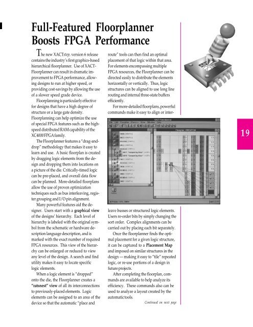
Full-Featured Floorplanner<br />
Boosts FPGA Performance<br />
The new XACTstep, version 6 release<br />
contains the industry’s first graphics-based<br />
hierarchical floorplanner. Use of XACT-<br />
Floorplanner can result in dramatic improvement<br />
to FPGA performance, allowing<br />
designs to run at higher speed, or<br />
providing cost-savings by allowing the use<br />
of a slower speed grade device.<br />
Floorplanning is particularly effective<br />
for designs that have a high degree of<br />
structure or a large gate density.<br />
Floorplanning can help optimize the use<br />
of special FPGA features such as the highspeed<br />
distributed RAM capability of the<br />
XC4000 FPGA family.<br />
The Floorplanner features a “drag-anddrop”<br />
methodology that makes it easy to<br />
learn and use. A basic floorplan is created<br />
by dragging logic elements from the design<br />
and dropping them into locations on<br />
a picture of the die. Critically-timed logic<br />
can be pre-placed, and overall data flow<br />
can be planned. More-detailed floorplans<br />
allow the use of proven optimization<br />
techniques such as bus interleaving, register<br />
grouping and I/O pin alignment.<br />
Many powerful features aid the designer.<br />
Users start with a graphical view<br />
of the designs’ hierarchy. Each level of<br />
hierarchy is labeled with the original symbol<br />
from the schematic or hardware description<br />
language description, and is<br />
marked with the exact number of required<br />
FPGA resources. This view of the hierarchy<br />
can be enlarged or reduced to view<br />
any level of the design. A search and find<br />
utility makes it easy to locate specific<br />
logic elements.<br />
When a logic element is “dropped”<br />
onto the die, the Floorplanner creates a<br />
“ratsnest” view of all its interconnections<br />
to previously-placed elements. Logic<br />
elements can be assigned to an area of the<br />
device so that the automatic “place and<br />
route” tools can then find an optimal<br />
placement of that logic within that area.<br />
For elements encompassing multiple<br />
FPGA resources, the Floorplanner can be<br />
directed easily to distribute the elements<br />
horizontally or vertically. Thus, logic<br />
structures can be aligned to use long line<br />
routing and internal three-state buffers<br />
efficiently.<br />
For more-detailed floorplans, powerful<br />
commands make it easy to align or inter-<br />
leave busses or structured logic elements.<br />
Users re-order bits by simply changing the<br />
sort order. Complex alignments can be<br />
carried out by placing each bit separately.<br />
Once the floorplanner finds the optimal<br />
placement for a given logic structure,<br />
it can be captured to a Placement Map<br />
and imposed on similar structures in the<br />
design — making it easy to “tile” repeated<br />
logic, or re-use portions of a design in<br />
future projects.<br />
After completing the floorplan, commands<br />
are available to help analyze its<br />
efficiency. These commands also can be<br />
used to analyze a layout created by the<br />
automatic tools.<br />
Continued on next page<br />
19


