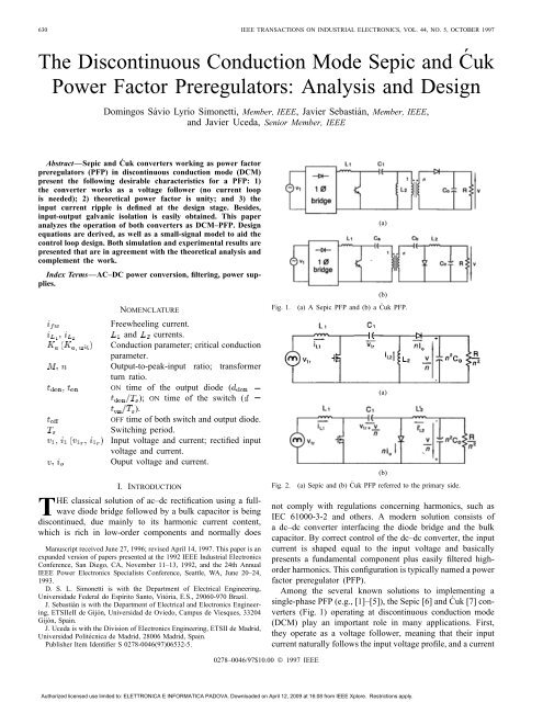
The Discontinuous Conduction Mode Sepic and ´ Cuk Power
The Discontinuous Conduction Mode Sepic and ´ Cuk Power
The Discontinuous Conduction Mode Sepic and ´ Cuk Power

Create successful ePaper yourself
Turn your PDF publications into a flip-book with our unique Google optimized e-Paper software.
630 IEEE TRANSACTIONS ON INDUSTRIAL ELECTRONICS, VOL. 44, NO. 5, OCTOBER 1997<br />
<strong>The</strong> <strong>Discontinuous</strong> <strong>Conduction</strong> <strong>Mode</strong> <strong>Sepic</strong> <strong>and</strong> Ćuk<br />
<strong>Power</strong> Factor Preregulators: Analysis <strong>and</strong> Design<br />
Domingos Sávio Lyrio Simonetti, Member, IEEE, Javier Sebastián, Member, IEEE,<br />
<strong>and</strong> Javier Uceda, Senior Member, IEEE<br />
Abstract—<strong>Sepic</strong> <strong>and</strong> Ćuk converters working as power factor<br />
preregulators (PFP) in discontinuous conduction mode (DCM)<br />
present the following desirable characteristics for a PFP: 1)<br />
the converter works as a voltage follower (no current loop<br />
is needed); 2) theoretical power factor is unity; <strong>and</strong> 3) the<br />
input current ripple is defined at the design stage. Besides,<br />
input-output galvanic isolation is easily obtained. This paper<br />
analyzes the operation of both converters as DCM–PFP. Design<br />
equations are derived, as well as a small-signal model to aid the<br />
control loop design. Both simulation <strong>and</strong> experimental results are<br />
presented that are in agreement with the theoretical analysis <strong>and</strong><br />
complement the work.<br />
Index Terms—AC–DC power conversion, filtering, power supplies.<br />
NOMENCLATURE<br />
Freewheeling current.<br />
<strong>and</strong> currents.<br />
<strong>Conduction</strong> parameter; critical conduction<br />
parameter.<br />
Output-to-peak-input ratio; transformer<br />
turn ratio.<br />
ON time of the output diode (<br />
); ON time of the switch (<br />
).<br />
OFF time of both switch <strong>and</strong> output diode.<br />
Switching period.<br />
Input voltage <strong>and</strong> current; rectified input<br />
voltage <strong>and</strong> current.<br />
Ouput voltage <strong>and</strong> current.<br />
I. INTRODUCTION<br />
THE classical solution of ac–dc rectification using a fullwave<br />
diode bridge followed by a bulk capacitor is being<br />
discontinued, due mainly to its harmonic current content,<br />
which is rich in low-order components <strong>and</strong> normally does<br />
Manuscript received June 27, 1996; revised April 14, 1997. This paper is an<br />
exp<strong>and</strong>ed version of papers presented at the 1992 IEEE Industrial Electronics<br />
Conference, San Diego, CA, November 11–13, 1992, <strong>and</strong> the 24th Annual<br />
IEEE <strong>Power</strong> Electronics Specialists Conference, Seattle, WA, June 20–24,<br />
1993.<br />
D. S. L. Simonetti is with the Department of Electrical Engineering,<br />
Universidade Federal do Espírito Santo, Vitória, E.S., 29060-970 Brazil.<br />
J. Sebastián is with the Department of Electrical <strong>and</strong> Electronics Engineering,<br />
ETSIIeII de Gijón, Universidad de Oviedo, Campus de Viesques, 33204<br />
Gijón, Spain.<br />
J. Uceda is with the Division of Electronics Engineering, ETSII de Madrid,<br />
Universidad Politécnica de Madrid, 28006 Madrid, Spain.<br />
Publisher Item Identifier S 0278-0046(97)06532-5.<br />
0278–0046/97$10.00 © 1997 IEEE<br />
(a)<br />
(b)<br />
Fig. 1. (a) A <strong>Sepic</strong> PFP <strong>and</strong> (b) a Ćuk PFP.<br />
(b)<br />
Fig. 2. (a) <strong>Sepic</strong> <strong>and</strong> (b) Ćuk PFP referred to the primary side.<br />
(a)<br />
not comply with regulations concerning harmonics, such as<br />
IEC 61000-3-2 <strong>and</strong> others. A modern solution consists of<br />
a dc–dc converter interfacing the diode bridge <strong>and</strong> the bulk<br />
capacitor. By correct control of the dc–dc converter, the input<br />
current is shaped equal to the input voltage <strong>and</strong> basically<br />
presents a fundamental component plus easily filtered highorder<br />
harmonics. This configuration is typically named a power<br />
factor preregulator (PFP).<br />
Among the several known solutions to implementing a<br />
single-phase PFP (e.g., [1]–[5]), the <strong>Sepic</strong> [6] <strong>and</strong> Ćuk [7] converters<br />
(Fig. 1) operating at discontinuous conduction mode<br />
(DCM) play an important role in many applications. First,<br />
they operate as a voltage follower, meaning that their input<br />
current naturally follows the input voltage profile, <strong>and</strong> a current<br />
Authorized licensed use limited to: ELETTRONICA E INFORMATICA PADOVA. Downloaded on April 12, 2009 at 16:08 from IEEE Xplore. Restrictions apply.
SIMONETTI et al.: SEPIC AND ĆUK POWER FACTOR PREREGULATORS 631<br />
(a) (b)<br />
(c) (d)<br />
Fig. 3. A <strong>Sepic</strong> DCM–PFP. (a) First stage of operation. (b) Second stage. (c) Third stage. (d) Inductor currents.<br />
loop is not necessary. Second, input–output isolation is easily<br />
implemented. Finally, the input current ripple is defined at<br />
the design stage by the correct choice of magnetic component<br />
values. <strong>The</strong> converters work with zero-current turn-on in the<br />
switch <strong>and</strong> zero-current turn-off in the output diode, but with<br />
high rms current <strong>and</strong> voltage stresses, which limits their<br />
application range. Also, it is necessary to consider inherent<br />
problems caused by an isolation transformer (e.g., leakage<br />
inductance) if one is used.<br />
In the following sections, the operating stages are presented<br />
for both converters as DCM–PFP’s, along with the design<br />
equations <strong>and</strong> a small-signal model. Some design examples,<br />
simulations, <strong>and</strong> experimental results complete the analysis.<br />
In this paper, DCM means that each switching period presents<br />
a time interval in which neither the switch nor the output diode<br />
is conducting (freewheeling stage).<br />
II. ANALYSIS OF OPERATION<br />
A <strong>Sepic</strong> PFP with input–output isolation is shown in<br />
Fig. 1(a), <strong>and</strong> a similar Ćuk PFP is shown in Fig. 1(b). In<br />
the analysis, the output stage is referred to the primary side of<br />
the transformer, <strong>and</strong> the resulting <strong>Sepic</strong> <strong>and</strong> Ćuk topologies are<br />
shown in Fig. 2(a) <strong>and</strong> (b), respectively. Because of space, in<br />
the following figures, only the <strong>Sepic</strong> operation is considered,<br />
but a similar development can be made for the Ćuk converter.<br />
Equations for both converters are identical, provided that, for<br />
the <strong>Sepic</strong> converter,<br />
<strong>and</strong> for the Ćuk converter,<br />
(1)<br />
(2)<br />
For the <strong>Sepic</strong> converter, the capacitor voltage is equal<br />
to the input voltage, whereas, for the Ćuk converter, it is the<br />
sum of input <strong>and</strong> (referred) output voltage.<br />
A. First Stage of Operation<br />
This stage is shown in Fig. 3(a). <strong>The</strong> inductor currents are<br />
defined as<br />
<strong>and</strong> can be seen in Fig. 3(d). This stage is defined by the ON<br />
time of the switch ( ).<br />
B. Second Stage of Operation<br />
<strong>The</strong> second stage is shown in Fig. 3(b), <strong>and</strong> <strong>and</strong><br />
are given by<br />
This stage finishes when <strong>and</strong> lasts<br />
Authorized licensed use limited to: ELETTRONICA E INFORMATICA PADOVA. Downloaded on April 12, 2009 at 16:08 from IEEE Xplore. Restrictions apply.<br />
(3)<br />
(4)<br />
(5)
632 IEEE TRANSACTIONS ON INDUSTRIAL ELECTRONICS, VOL. 44, NO. 5, OCTOBER 1997<br />
Fig. 4. Diode current.<br />
C. Third Stage of Operation<br />
This is a freewheeling stage, shown in Fig. 3(c). This stage<br />
lasts until the start of a new switching period. <strong>The</strong> switch <strong>and</strong><br />
output diode OFF time is given by<br />
D. Average Output Current<br />
For both converters, the average output current is the<br />
average diode current, shown in Fig. 4. Its peak value is given<br />
by<br />
where<br />
Its average value in a switching period is given by<br />
<strong>and</strong> the average for half of a line period becomes<br />
E. Input Current<br />
Considering 100% of efficiency, ,<br />
Using (9) in (11), <strong>and</strong> noting that ,<br />
where<br />
(6)<br />
(7)<br />
(8)<br />
(9)<br />
(10)<br />
(11)<br />
(12)<br />
(13)<br />
Fig. 5. Input current ripple.<br />
From (12), it can be seen that <strong>Sepic</strong> <strong>and</strong> Ćuk converters<br />
as DCM–PFP are perfect PFP in theory ( is perfectly<br />
sinusoidal).<br />
F. <strong>Discontinuous</strong> <strong>Conduction</strong> <strong>Mode</strong> Operation<br />
<strong>and</strong> the Critical <strong>Conduction</strong> Parameter<br />
To operate at DCM, the following inequalities must hold<br />
[see Fig. 3(d)]:<br />
(14)<br />
(15)<br />
<strong>The</strong> worst situation occurs for . <strong>The</strong>refore, to<br />
operate at DCM,<br />
On the other h<strong>and</strong>, the average output current is given by<br />
Using (10) <strong>and</strong> (17) results in<br />
(16)<br />
(17)<br />
(18)<br />
where is the conduction parameter of the <strong>Sepic</strong> or Ćuk<br />
PFP:<br />
(19)<br />
From (16) <strong>and</strong> (18), the critical value of to<br />
operate at DCM [8] can be found as<br />
(20)<br />
G. <strong>and</strong> Design<br />
<strong>The</strong> equivalent inductance<br />
is given by<br />
is obtained using (19) <strong>and</strong><br />
(21)<br />
<strong>The</strong> design of <strong>and</strong> is made using the desired ripple<br />
value of the input current. Considering the input current shown<br />
in Fig. 5, its peak-to-peak value is given as<br />
Its maximum value occurs for <strong>and</strong> is given by<br />
Authorized licensed use limited to: ELETTRONICA E INFORMATICA PADOVA. Downloaded on April 12, 2009 at 16:08 from IEEE Xplore. Restrictions apply.<br />
(22)<br />
(23)
SIMONETTI et al.: SEPIC AND ĆUK POWER FACTOR PREREGULATORS 633<br />
<strong>The</strong>refore, can be obtained considering the specified<br />
maximum current ripple:<br />
<strong>and</strong><br />
(24)<br />
(25)<br />
( normally is a percentage of the fundamental input current<br />
.)<br />
H. <strong>The</strong> Design of the Intermediate Capacitor<br />
In conventional <strong>Sepic</strong> <strong>and</strong> Ćuk converters, the capacitor<br />
voltage is assumed to be constant. When operating as a PFP,<br />
the capacitor voltage is under the following two conflicting<br />
constraints: 1) to present a nearly constant value within a<br />
switching period <strong>and</strong> 2) to follow the input voltage profile<br />
within a line period. Its value has a significant influence in the<br />
input current waveform. <strong>The</strong> resonant frequency of , ,<br />
<strong>and</strong> must be much greater than the line frequency to avoid<br />
input current oscillations at every line half cycle. Also, the<br />
resonant frequency between <strong>and</strong> must be lower than<br />
the switching frequency to assure almost constant voltage in<br />
a switching period. A good initial approximation for is<br />
given by [9]<br />
where<br />
(26)<br />
(27)<br />
An isolated Ćuk converter presents an additional resonance<br />
caused by the transformer magnetizing inductance that might<br />
constitute a major problem [10]. In the <strong>Sepic</strong> converter, the<br />
magnetizing inductance is usually used as the inductor .<br />
I. Small-Signal <strong>Mode</strong>l<br />
A small-signal model can be easily obtained using the<br />
CIECA approach [11]. <strong>The</strong> following small-signal perturbations<br />
will be applied to both input <strong>and</strong> output average currents:<br />
where the caret means steady-state value <strong>and</strong> means<br />
the introduced perturbation (small-signal value). Applying<br />
the perturbations in (10) <strong>and</strong> performing the small-signal<br />
approximation ( ) results in<br />
(28)<br />
Fig. 6. Small-signal model equivalent circuit.<br />
where<br />
Repeating the procedure for (13) results in<br />
where<br />
(29)<br />
(30)<br />
(31)<br />
<strong>The</strong> equivalent electric circuit described by (28) <strong>and</strong> (30)<br />
is shown in Fig. 6. From the equivalent circuit, the transfer<br />
function for the particular application can be found. <strong>The</strong><br />
equivalent small-signal impedance of the load is a function<br />
of the type of load the PFP is feeding.<br />
1) Constant Impedance Load: <strong>The</strong> small-signal impedance<br />
is the actual load impedance:<br />
(32)<br />
2) Constant <strong>Power</strong> Load: A PFP usually feeds a dc–dc<br />
converter [(switch-mode power supply (SMPS)]. An SMPS<br />
presents the following small-signal input impedance [12]:<br />
(33)<br />
3) Constant Current Load: <strong>The</strong> load acts as a current<br />
source (e.g., a linear regulator). <strong>The</strong> small-signal impedance is<br />
(34)<br />
III. DESIGN EXAMPLE AND SIMULATION<br />
A <strong>Sepic</strong> PFP was designed with the following characteristics:<br />
t V;<br />
V;<br />
kHz s<br />
W<br />
Authorized licensed use limited to: ELETTRONICA E INFORMATICA PADOVA. Downloaded on April 12, 2009 at 16:08 from IEEE Xplore. Restrictions apply.
634 IEEE TRANSACTIONS ON INDUSTRIAL ELECTRONICS, VOL. 44, NO. 5, OCTOBER 1997<br />
(a) (b)<br />
(c) (d)<br />
Fig. 7. Simulation results. (a) Input current. (b) Inductor currents. (c) Output voltage. (d) Intermediate capacitor (gI) voltage.<br />
<strong>The</strong> ratio is<br />
(35)<br />
<strong>The</strong> critical conduction parameter (boundary between discontinuous<br />
<strong>and</strong> continuous conduction operation) is<br />
(36)<br />
To assure DCM operation, the following is<br />
chosen:<br />
From (18), the nominal duty cycle is found:<br />
<strong>and</strong>, using (21),<br />
<strong>The</strong> current ripple is<br />
(37)<br />
(38)<br />
H (39)<br />
A (40)<br />
<strong>and</strong>, from (24) <strong>and</strong> (25),<br />
mH<br />
H (41)<br />
Considering a resonant frequency of 2500 [Hz] the intermediate<br />
capacitor is given by<br />
F (42)<br />
Through simulation, was chosen to be 0.39 F. Simulation<br />
results are shown in Fig. 7. Fig. 7(a) shows the input<br />
current; Fig. 7(b) shows the current in inductors <strong>and</strong> for<br />
a few switching periods; Fig. 7(c) shows the output voltage<br />
<strong>and</strong> Fig. 7(d) shows capacitor voltage.<br />
<strong>The</strong> importance of a correct choice of capacitor is shown<br />
in Fig. 8. Fig. 8(a) shows the input current using F;<br />
a low-frequency oscillation ( kHz) can be observed<br />
in the current signal. On the other h<strong>and</strong>, Fig. 8(b) shows<br />
the capacitor voltage for F. In this case, the<br />
capacitor voltage cannot be considered constant in a switching<br />
period, <strong>and</strong> its peak value is much higher than that shown<br />
in Fig. 7(d).<br />
Authorized licensed use limited to: ELETTRONICA E INFORMATICA PADOVA. Downloaded on April 12, 2009 at 16:08 from IEEE Xplore. Restrictions apply.
SIMONETTI et al.: SEPIC AND ĆUK POWER FACTOR PREREGULATORS 635<br />
(a)<br />
(b)<br />
Fig. 8. Influence of gI value. (a) Input current using gI a QXW "F. (b) gI<br />
capacitor voltage using gI aHXI"F.<br />
Also, the small-signal model was tested through simulation.<br />
From (29), it is found that<br />
(43)<br />
Considering a resistive load, <strong>and</strong> having mF, the<br />
transfer function is<br />
(44)<br />
Fig. 9(a) shows full-circuit simulation <strong>and</strong> small-signal<br />
model results for a 20-V increase in the input voltage<br />
( ). For a constant power load, the transfer function<br />
is given by<br />
(45)<br />
Fig. 9(b) shows open-loop simulation <strong>and</strong> model results<br />
for a change of 10% in the duty cycle ( ). <strong>The</strong><br />
estimated small-signal model results <strong>and</strong> full-circuit simulation<br />
results are in good agreement. Simulation results have shown<br />
the validity of the design approach <strong>and</strong> small-signal model<br />
presented.<br />
(a)<br />
(b)<br />
Fig. 9. Open-loop dynamic simulation results. (a) Input voltage increased by<br />
20 V, resistive load. (b) Duty-cycle increased by 0.03, constant power load.<br />
IV. EXPERIMENTAL RESULTS<br />
<strong>The</strong> following single-phase <strong>Sepic</strong> DCM–PFP was implemented:<br />
V;<br />
kHz;<br />
W;<br />
t V;<br />
Using the equations presented in this paper, the following<br />
is obtained:<br />
Authorized licensed use limited to: ELETTRONICA E INFORMATICA PADOVA. Downloaded on April 12, 2009 at 16:08 from IEEE Xplore. Restrictions apply.<br />
mH<br />
H<br />
F (46)
636 IEEE TRANSACTIONS ON INDUSTRIAL ELECTRONICS, VOL. 44, NO. 5, OCTOBER 1997<br />
(a) (b)<br />
(c) (d)<br />
Fig. 10. Experimental results. (a) Input voltage <strong>and</strong> current (filtered). (b) Inductor currents. (c) Output voltage. (d) Dynamic response for a load change.<br />
<strong>The</strong> control-to-output transfer function ( F) is<br />
(47)<br />
<strong>The</strong> feedback loop of a PFP must be slow (crossover<br />
frequency below one-third of the line frequency) to avoid excessive<br />
second-harmonic injection from the output voltage into<br />
the input current (resulting in third-order harmonic current) [1].<br />
<strong>The</strong> system is stable if the open-loop transfer function crosses<br />
0 dB with 20 dB slope. Taking these points into account, an<br />
output voltage feedback loop was implemented, yielding the<br />
following open-loop transfer function:<br />
(48)<br />
<strong>The</strong> zero crossover frequency is about 5 Hz with 20 dB<br />
slope, <strong>and</strong> the gain at 100 Hz is close to 0.01.<br />
Fig. 10(a) shows the converter input voltage <strong>and</strong> current.<br />
It can be observed that the current actually follows the input<br />
voltage. Fig. 10(b) shows <strong>and</strong> inductor currents for a<br />
few switching periods, whereas Fig. 10(c) shows the output<br />
voltage. <strong>The</strong> dynamic response of the PFP for a 100–50 W load<br />
change <strong>and</strong> vice versa can be seen in Fig. 10(d). Experimental<br />
results confirm the analysis carried out in this paper.<br />
V. CONCLUSIONS<br />
<strong>Sepic</strong> <strong>and</strong> Ćuk converters working as PFP in DCM are<br />
perfect preregulators. <strong>The</strong> input current naturally follows the<br />
input voltage, <strong>and</strong> theoretical power factor is one. <strong>The</strong> operation<br />
analysis for each stage leads to the equations for<br />
correctly designing the converter. <strong>The</strong> ripple present in the<br />
input current is limited by design, choosing an adequate<br />
value for the input inductor ( ). A correct choice of the<br />
intermediate capacitor is fundamental in obtaining a highquality<br />
input current.<br />
<strong>The</strong> static <strong>and</strong> dynamic simulation results, as well as the experimental<br />
results, have confirmed the validity of the analysis<br />
<strong>and</strong> design approaches presented here.<br />
REFERENCES<br />
[1] L. H. Dixon, “High power factor preregulators for off-line power<br />
supplies,” in Unitrode <strong>Power</strong> Supply Design Seminar Manual SEM600,<br />
Unitrode Corp., Waltham, MA, pp. 6.1–6.16, 1988.<br />
[2] I. Barbi <strong>and</strong> S. A. O. Silva, “Sinusoidal line current rectification at<br />
unity power factor with boost quasiresonant converters,” in Proc. IEEE<br />
APEC, 1990, pp. 553–562.<br />
[3] C. Zhov, R. B. Ridley, <strong>and</strong> F. C. Lee, “Design <strong>and</strong> analysis of a<br />
hysteretic boost power factor correction circuit,” in Proc. IEEE PESC,<br />
1990, pp. 800–807.<br />
[4] J. Sebastián, J. Uceda, J. A. Cobos, J. Arau, <strong>and</strong> F. Aldana, “Improving<br />
power factor correction in distributed power supply systems using<br />
PWM <strong>and</strong> ZCS-QR <strong>Sepic</strong> topologies,” in Proc. IEEE PESC, 1991, pp.<br />
780–791.<br />
Authorized licensed use limited to: ELETTRONICA E INFORMATICA PADOVA. Downloaded on April 12, 2009 at 16:08 from IEEE Xplore. Restrictions apply.
SIMONETTI et al.: SEPIC AND ĆUK POWER FACTOR PREREGULATORS 637<br />
[5] R. Erickson, M. Madigan, <strong>and</strong> S. Singer, “Design of a simple highpower-factor<br />
rectifier based on the flyback converter,” in Proc. IEEE<br />
APEC, 1990, pp. 792–801.<br />
[6] R. P. Massey <strong>and</strong> E. C. Snyder, “High voltage single-ended DC–DC<br />
converter,” in Proc. IEEE PESC, 1977, pp. 156–159.<br />
[7] S. Ćuk <strong>and</strong> R. D. Middlebrook, “A new optimum topology switching<br />
DC-to-DC converter,” in Proc. IEEE PESC, 1977, pp. 160–179.<br />
[8] J. Sebastián, J. A. Cobos, P. Gil, <strong>and</strong> J. Uceda, “<strong>The</strong> determination of<br />
the boundaries between continuous <strong>and</strong> discontinuous conduction modes<br />
in DC-to-DC converters used as power factor preregulators,” in Proc.<br />
IEEE PESC, 1992, pp. 1061–1070.<br />
[9] D. S. L. Simonetti, “AC–DC preregulators with power factor<br />
correction—Single-switch solutions,” Ph.D. dissertation, Univ.<br />
Politécnica de Madrid, Madrid, Spain, Nov. 1995.<br />
[10] R. A. Langley, J. D. van Wyk, <strong>and</strong> J. J. Schoeman, “Instabilities in<br />
transformer-coupled Ćuk-converters <strong>and</strong> their solution at higher power<br />
levels,” in Proc. 4th Int. Conf. <strong>Power</strong> Electronics <strong>and</strong> Variable-Speed<br />
Drives, July 1990, pp. 207–211.<br />
[11] P. R. K. Chetty, “Current injected equivalent circuit approach (CIECA)<br />
to modeling of switching dc–dc converters,” IEEE Trans. Aerosp.<br />
Electron. Syst., vol. 17, pp. 802–808, Nov. 1981.<br />
[12] R. D. Middlebrook, “Input filter considerations in design <strong>and</strong> application<br />
of switching regulators,” in Conf. Rec. IEEE-IAS Annu. Meeting, 1979,<br />
pp. 366–382.<br />
Domingos Sávio Lyrio Simonetti (S’92–M’95)<br />
was born in Vitória, Brazil, in 1961. He received<br />
the Degree in electrical engineering from the<br />
Universidade Federal do Espírito Santo, Vitória,<br />
Brazil, the M.Sc. degree from the Federal University<br />
of Santa Catarina, Florianópolis, Brazil, <strong>and</strong> the<br />
Ph.D. degree from the Universidad Politécnica de<br />
Madrid, Madrid, Spain, in 1984, 1987, <strong>and</strong> 1995,<br />
respectively.<br />
Since 1984, he has been a Professor in the<br />
Electrical Engineering Department, Universidade<br />
Federal do Espírito Santo. His research interests include high-power-factor<br />
rectifiers, active power filters, low-loss converters, <strong>and</strong> machine drives.<br />
Javier Sebastián (M’87), for a photograph <strong>and</strong> biography, see this issue,<br />
p. 603.<br />
Javier Uceda (M’83–SM’91), for a photograph <strong>and</strong> biography, see this issue,<br />
p. 603.<br />
Authorized licensed use limited to: ELETTRONICA E INFORMATICA PADOVA. Downloaded on April 12, 2009 at 16:08 from IEEE Xplore. Restrictions apply.