The Discontinuous Conduction Mode Sepic and ´ Cuk Power
The Discontinuous Conduction Mode Sepic and ´ Cuk Power
The Discontinuous Conduction Mode Sepic and ´ Cuk Power

You also want an ePaper? Increase the reach of your titles
YUMPU automatically turns print PDFs into web optimized ePapers that Google loves.
630 IEEE TRANSACTIONS ON INDUSTRIAL ELECTRONICS, VOL. 44, NO. 5, OCTOBER 1997<br />
<strong>The</strong> <strong>Discontinuous</strong> <strong>Conduction</strong> <strong>Mode</strong> <strong>Sepic</strong> <strong>and</strong> Ćuk<br />
<strong>Power</strong> Factor Preregulators: Analysis <strong>and</strong> Design<br />
Domingos Sávio Lyrio Simonetti, Member, IEEE, Javier Sebastián, Member, IEEE,<br />
<strong>and</strong> Javier Uceda, Senior Member, IEEE<br />
Abstract—<strong>Sepic</strong> <strong>and</strong> Ćuk converters working as power factor<br />
preregulators (PFP) in discontinuous conduction mode (DCM)<br />
present the following desirable characteristics for a PFP: 1)<br />
the converter works as a voltage follower (no current loop<br />
is needed); 2) theoretical power factor is unity; <strong>and</strong> 3) the<br />
input current ripple is defined at the design stage. Besides,<br />
input-output galvanic isolation is easily obtained. This paper<br />
analyzes the operation of both converters as DCM–PFP. Design<br />
equations are derived, as well as a small-signal model to aid the<br />
control loop design. Both simulation <strong>and</strong> experimental results are<br />
presented that are in agreement with the theoretical analysis <strong>and</strong><br />
complement the work.<br />
Index Terms—AC–DC power conversion, filtering, power supplies.<br />
NOMENCLATURE<br />
Freewheeling current.<br />
<strong>and</strong> currents.<br />
<strong>Conduction</strong> parameter; critical conduction<br />
parameter.<br />
Output-to-peak-input ratio; transformer<br />
turn ratio.<br />
ON time of the output diode (<br />
); ON time of the switch (<br />
).<br />
OFF time of both switch <strong>and</strong> output diode.<br />
Switching period.<br />
Input voltage <strong>and</strong> current; rectified input<br />
voltage <strong>and</strong> current.<br />
Ouput voltage <strong>and</strong> current.<br />
I. INTRODUCTION<br />
THE classical solution of ac–dc rectification using a fullwave<br />
diode bridge followed by a bulk capacitor is being<br />
discontinued, due mainly to its harmonic current content,<br />
which is rich in low-order components <strong>and</strong> normally does<br />
Manuscript received June 27, 1996; revised April 14, 1997. This paper is an<br />
exp<strong>and</strong>ed version of papers presented at the 1992 IEEE Industrial Electronics<br />
Conference, San Diego, CA, November 11–13, 1992, <strong>and</strong> the 24th Annual<br />
IEEE <strong>Power</strong> Electronics Specialists Conference, Seattle, WA, June 20–24,<br />
1993.<br />
D. S. L. Simonetti is with the Department of Electrical Engineering,<br />
Universidade Federal do Espírito Santo, Vitória, E.S., 29060-970 Brazil.<br />
J. Sebastián is with the Department of Electrical <strong>and</strong> Electronics Engineering,<br />
ETSIIeII de Gijón, Universidad de Oviedo, Campus de Viesques, 33204<br />
Gijón, Spain.<br />
J. Uceda is with the Division of Electronics Engineering, ETSII de Madrid,<br />
Universidad Politécnica de Madrid, 28006 Madrid, Spain.<br />
Publisher Item Identifier S 0278-0046(97)06532-5.<br />
0278–0046/97$10.00 © 1997 IEEE<br />
(a)<br />
(b)<br />
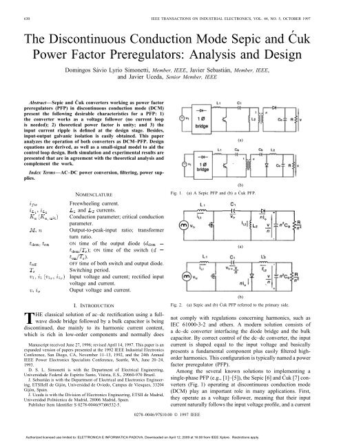
Fig. 1. (a) A <strong>Sepic</strong> PFP <strong>and</strong> (b) a Ćuk PFP.<br />
(b)<br />
Fig. 2. (a) <strong>Sepic</strong> <strong>and</strong> (b) Ćuk PFP referred to the primary side.<br />
(a)<br />
not comply with regulations concerning harmonics, such as<br />
IEC 61000-3-2 <strong>and</strong> others. A modern solution consists of<br />
a dc–dc converter interfacing the diode bridge <strong>and</strong> the bulk<br />
capacitor. By correct control of the dc–dc converter, the input<br />
current is shaped equal to the input voltage <strong>and</strong> basically<br />
presents a fundamental component plus easily filtered highorder<br />
harmonics. This configuration is typically named a power<br />
factor preregulator (PFP).<br />
Among the several known solutions to implementing a<br />
single-phase PFP (e.g., [1]–[5]), the <strong>Sepic</strong> [6] <strong>and</strong> Ćuk [7] converters<br />
(Fig. 1) operating at discontinuous conduction mode<br />
(DCM) play an important role in many applications. First,<br />
they operate as a voltage follower, meaning that their input<br />
current naturally follows the input voltage profile, <strong>and</strong> a current<br />
Authorized licensed use limited to: ELETTRONICA E INFORMATICA PADOVA. Downloaded on April 12, 2009 at 16:08 from IEEE Xplore. Restrictions apply.
SIMONETTI et al.: SEPIC AND ĆUK POWER FACTOR PREREGULATORS 631<br />
(a) (b)<br />
(c) (d)<br />
Fig. 3. A <strong>Sepic</strong> DCM–PFP. (a) First stage of operation. (b) Second stage. (c) Third stage. (d) Inductor currents.<br />
loop is not necessary. Second, input–output isolation is easily<br />
implemented. Finally, the input current ripple is defined at<br />
the design stage by the correct choice of magnetic component<br />
values. <strong>The</strong> converters work with zero-current turn-on in the<br />
switch <strong>and</strong> zero-current turn-off in the output diode, but with<br />
high rms current <strong>and</strong> voltage stresses, which limits their<br />
application range. Also, it is necessary to consider inherent<br />
problems caused by an isolation transformer (e.g., leakage<br />
inductance) if one is used.<br />
In the following sections, the operating stages are presented<br />
for both converters as DCM–PFP’s, along with the design<br />
equations <strong>and</strong> a small-signal model. Some design examples,<br />
simulations, <strong>and</strong> experimental results complete the analysis.<br />
In this paper, DCM means that each switching period presents<br />
a time interval in which neither the switch nor the output diode<br />
is conducting (freewheeling stage).<br />
II. ANALYSIS OF OPERATION<br />
A <strong>Sepic</strong> PFP with input–output isolation is shown in<br />
Fig. 1(a), <strong>and</strong> a similar Ćuk PFP is shown in Fig. 1(b). In<br />
the analysis, the output stage is referred to the primary side of<br />
the transformer, <strong>and</strong> the resulting <strong>Sepic</strong> <strong>and</strong> Ćuk topologies are<br />
shown in Fig. 2(a) <strong>and</strong> (b), respectively. Because of space, in<br />
the following figures, only the <strong>Sepic</strong> operation is considered,<br />
but a similar development can be made for the Ćuk converter.<br />
Equations for both converters are identical, provided that, for<br />
the <strong>Sepic</strong> converter,<br />
<strong>and</strong> for the Ćuk converter,<br />
(1)<br />
(2)<br />
For the <strong>Sepic</strong> converter, the capacitor voltage is equal<br />
to the input voltage, whereas, for the Ćuk converter, it is the<br />
sum of input <strong>and</strong> (referred) output voltage.<br />
A. First Stage of Operation<br />
This stage is shown in Fig. 3(a). <strong>The</strong> inductor currents are<br />
defined as<br />
<strong>and</strong> can be seen in Fig. 3(d). This stage is defined by the ON<br />
time of the switch ( ).<br />
B. Second Stage of Operation<br />
<strong>The</strong> second stage is shown in Fig. 3(b), <strong>and</strong> <strong>and</strong><br />
are given by<br />
This stage finishes when <strong>and</strong> lasts<br />
Authorized licensed use limited to: ELETTRONICA E INFORMATICA PADOVA. Downloaded on April 12, 2009 at 16:08 from IEEE Xplore. Restrictions apply.<br />
(3)<br />
(4)<br />
(5)
632 IEEE TRANSACTIONS ON INDUSTRIAL ELECTRONICS, VOL. 44, NO. 5, OCTOBER 1997<br />
Fig. 4. Diode current.<br />
C. Third Stage of Operation<br />
This is a freewheeling stage, shown in Fig. 3(c). This stage<br />
lasts until the start of a new switching period. <strong>The</strong> switch <strong>and</strong><br />
output diode OFF time is given by<br />
D. Average Output Current<br />
For both converters, the average output current is the<br />
average diode current, shown in Fig. 4. Its peak value is given<br />
by<br />
where<br />
Its average value in a switching period is given by<br />
<strong>and</strong> the average for half of a line period becomes<br />
E. Input Current<br />
Considering 100% of efficiency, ,<br />
Using (9) in (11), <strong>and</strong> noting that ,<br />
where<br />
(6)<br />
(7)<br />
(8)<br />
(9)<br />
(10)<br />
(11)<br />
(12)<br />
(13)<br />
Fig. 5. Input current ripple.<br />
From (12), it can be seen that <strong>Sepic</strong> <strong>and</strong> Ćuk converters<br />
as DCM–PFP are perfect PFP in theory ( is perfectly<br />
sinusoidal).<br />
F. <strong>Discontinuous</strong> <strong>Conduction</strong> <strong>Mode</strong> Operation<br />
<strong>and</strong> the Critical <strong>Conduction</strong> Parameter<br />
To operate at DCM, the following inequalities must hold<br />
[see Fig. 3(d)]:<br />
(14)<br />
(15)<br />
<strong>The</strong> worst situation occurs for . <strong>The</strong>refore, to<br />
operate at DCM,<br />
On the other h<strong>and</strong>, the average output current is given by<br />
Using (10) <strong>and</strong> (17) results in<br />
(16)<br />
(17)<br />
(18)<br />
where is the conduction parameter of the <strong>Sepic</strong> or Ćuk<br />
PFP:<br />
(19)<br />
From (16) <strong>and</strong> (18), the critical value of to<br />
operate at DCM [8] can be found as<br />
(20)<br />
G. <strong>and</strong> Design<br />
<strong>The</strong> equivalent inductance<br />
is given by<br />
is obtained using (19) <strong>and</strong><br />
(21)<br />
<strong>The</strong> design of <strong>and</strong> is made using the desired ripple<br />
value of the input current. Considering the input current shown<br />
in Fig. 5, its peak-to-peak value is given as<br />
Its maximum value occurs for <strong>and</strong> is given by<br />
Authorized licensed use limited to: ELETTRONICA E INFORMATICA PADOVA. Downloaded on April 12, 2009 at 16:08 from IEEE Xplore. Restrictions apply.<br />
(22)<br />
(23)
SIMONETTI et al.: SEPIC AND ĆUK POWER FACTOR PREREGULATORS 633<br />
<strong>The</strong>refore, can be obtained considering the specified<br />
maximum current ripple:<br />
<strong>and</strong><br />
(24)<br />
(25)<br />
( normally is a percentage of the fundamental input current<br />
.)<br />
H. <strong>The</strong> Design of the Intermediate Capacitor<br />
In conventional <strong>Sepic</strong> <strong>and</strong> Ćuk converters, the capacitor<br />
voltage is assumed to be constant. When operating as a PFP,<br />
the capacitor voltage is under the following two conflicting<br />
constraints: 1) to present a nearly constant value within a<br />
switching period <strong>and</strong> 2) to follow the input voltage profile<br />
within a line period. Its value has a significant influence in the<br />
input current waveform. <strong>The</strong> resonant frequency of , ,<br />
<strong>and</strong> must be much greater than the line frequency to avoid<br />
input current oscillations at every line half cycle. Also, the<br />
resonant frequency between <strong>and</strong> must be lower than<br />
the switching frequency to assure almost constant voltage in<br />
a switching period. A good initial approximation for is<br />
given by [9]<br />
where<br />
(26)<br />
(27)<br />
An isolated Ćuk converter presents an additional resonance<br />
caused by the transformer magnetizing inductance that might<br />
constitute a major problem [10]. In the <strong>Sepic</strong> converter, the<br />
magnetizing inductance is usually used as the inductor .<br />
I. Small-Signal <strong>Mode</strong>l<br />
A small-signal model can be easily obtained using the<br />
CIECA approach [11]. <strong>The</strong> following small-signal perturbations<br />
will be applied to both input <strong>and</strong> output average currents:<br />
where the caret means steady-state value <strong>and</strong> means<br />
the introduced perturbation (small-signal value). Applying<br />
the perturbations in (10) <strong>and</strong> performing the small-signal<br />
approximation ( ) results in<br />
(28)<br />
Fig. 6. Small-signal model equivalent circuit.<br />
where<br />
Repeating the procedure for (13) results in<br />
where<br />
(29)<br />
(30)<br />
(31)<br />
<strong>The</strong> equivalent electric circuit described by (28) <strong>and</strong> (30)<br />
is shown in Fig. 6. From the equivalent circuit, the transfer<br />
function for the particular application can be found. <strong>The</strong><br />
equivalent small-signal impedance of the load is a function<br />
of the type of load the PFP is feeding.<br />
1) Constant Impedance Load: <strong>The</strong> small-signal impedance<br />
is the actual load impedance:<br />
(32)<br />
2) Constant <strong>Power</strong> Load: A PFP usually feeds a dc–dc<br />
converter [(switch-mode power supply (SMPS)]. An SMPS<br />
presents the following small-signal input impedance [12]:<br />
(33)<br />
3) Constant Current Load: <strong>The</strong> load acts as a current<br />
source (e.g., a linear regulator). <strong>The</strong> small-signal impedance is<br />
(34)<br />
III. DESIGN EXAMPLE AND SIMULATION<br />
A <strong>Sepic</strong> PFP was designed with the following characteristics:<br />
t V;<br />
V;<br />
kHz s<br />
W<br />
Authorized licensed use limited to: ELETTRONICA E INFORMATICA PADOVA. Downloaded on April 12, 2009 at 16:08 from IEEE Xplore. Restrictions apply.
634 IEEE TRANSACTIONS ON INDUSTRIAL ELECTRONICS, VOL. 44, NO. 5, OCTOBER 1997<br />
(a) (b)<br />
(c) (d)<br />
Fig. 7. Simulation results. (a) Input current. (b) Inductor currents. (c) Output voltage. (d) Intermediate capacitor (gI) voltage.<br />
<strong>The</strong> ratio is<br />
(35)<br />
<strong>The</strong> critical conduction parameter (boundary between discontinuous<br />
<strong>and</strong> continuous conduction operation) is<br />
(36)<br />
To assure DCM operation, the following is<br />
chosen:<br />
From (18), the nominal duty cycle is found:<br />
<strong>and</strong>, using (21),<br />
<strong>The</strong> current ripple is<br />
(37)<br />
(38)<br />
H (39)<br />
A (40)<br />
<strong>and</strong>, from (24) <strong>and</strong> (25),<br />
mH<br />
H (41)<br />
Considering a resonant frequency of 2500 [Hz] the intermediate<br />
capacitor is given by<br />
F (42)<br />
Through simulation, was chosen to be 0.39 F. Simulation<br />
results are shown in Fig. 7. Fig. 7(a) shows the input<br />
current; Fig. 7(b) shows the current in inductors <strong>and</strong> for<br />
a few switching periods; Fig. 7(c) shows the output voltage<br />
<strong>and</strong> Fig. 7(d) shows capacitor voltage.<br />
<strong>The</strong> importance of a correct choice of capacitor is shown<br />
in Fig. 8. Fig. 8(a) shows the input current using F;<br />
a low-frequency oscillation ( kHz) can be observed<br />
in the current signal. On the other h<strong>and</strong>, Fig. 8(b) shows<br />
the capacitor voltage for F. In this case, the<br />
capacitor voltage cannot be considered constant in a switching<br />
period, <strong>and</strong> its peak value is much higher than that shown<br />
in Fig. 7(d).<br />
Authorized licensed use limited to: ELETTRONICA E INFORMATICA PADOVA. Downloaded on April 12, 2009 at 16:08 from IEEE Xplore. Restrictions apply.
SIMONETTI et al.: SEPIC AND ĆUK POWER FACTOR PREREGULATORS 635<br />
(a)<br />
(b)<br />
Fig. 8. Influence of gI value. (a) Input current using gI a QXW "F. (b) gI<br />
capacitor voltage using gI aHXI"F.<br />
Also, the small-signal model was tested through simulation.<br />
From (29), it is found that<br />
(43)<br />
Considering a resistive load, <strong>and</strong> having mF, the<br />
transfer function is<br />
(44)<br />
Fig. 9(a) shows full-circuit simulation <strong>and</strong> small-signal<br />
model results for a 20-V increase in the input voltage<br />
( ). For a constant power load, the transfer function<br />
is given by<br />
(45)<br />
Fig. 9(b) shows open-loop simulation <strong>and</strong> model results<br />
for a change of 10% in the duty cycle ( ). <strong>The</strong><br />
estimated small-signal model results <strong>and</strong> full-circuit simulation<br />
results are in good agreement. Simulation results have shown<br />
the validity of the design approach <strong>and</strong> small-signal model<br />
presented.<br />
(a)<br />
(b)<br />
Fig. 9. Open-loop dynamic simulation results. (a) Input voltage increased by<br />
20 V, resistive load. (b) Duty-cycle increased by 0.03, constant power load.<br />
IV. EXPERIMENTAL RESULTS<br />
<strong>The</strong> following single-phase <strong>Sepic</strong> DCM–PFP was implemented:<br />
V;<br />
kHz;<br />
W;<br />
t V;<br />
Using the equations presented in this paper, the following<br />
is obtained:<br />
Authorized licensed use limited to: ELETTRONICA E INFORMATICA PADOVA. Downloaded on April 12, 2009 at 16:08 from IEEE Xplore. Restrictions apply.<br />
mH<br />
H<br />
F (46)
636 IEEE TRANSACTIONS ON INDUSTRIAL ELECTRONICS, VOL. 44, NO. 5, OCTOBER 1997<br />
(a) (b)<br />
(c) (d)<br />
Fig. 10. Experimental results. (a) Input voltage <strong>and</strong> current (filtered). (b) Inductor currents. (c) Output voltage. (d) Dynamic response for a load change.<br />
<strong>The</strong> control-to-output transfer function ( F) is<br />
(47)<br />
<strong>The</strong> feedback loop of a PFP must be slow (crossover<br />
frequency below one-third of the line frequency) to avoid excessive<br />
second-harmonic injection from the output voltage into<br />
the input current (resulting in third-order harmonic current) [1].<br />
<strong>The</strong> system is stable if the open-loop transfer function crosses<br />
0 dB with 20 dB slope. Taking these points into account, an<br />
output voltage feedback loop was implemented, yielding the<br />
following open-loop transfer function:<br />
(48)<br />
<strong>The</strong> zero crossover frequency is about 5 Hz with 20 dB<br />
slope, <strong>and</strong> the gain at 100 Hz is close to 0.01.<br />
Fig. 10(a) shows the converter input voltage <strong>and</strong> current.<br />
It can be observed that the current actually follows the input<br />
voltage. Fig. 10(b) shows <strong>and</strong> inductor currents for a<br />
few switching periods, whereas Fig. 10(c) shows the output<br />
voltage. <strong>The</strong> dynamic response of the PFP for a 100–50 W load<br />
change <strong>and</strong> vice versa can be seen in Fig. 10(d). Experimental<br />
results confirm the analysis carried out in this paper.<br />
V. CONCLUSIONS<br />
<strong>Sepic</strong> <strong>and</strong> Ćuk converters working as PFP in DCM are<br />
perfect preregulators. <strong>The</strong> input current naturally follows the<br />
input voltage, <strong>and</strong> theoretical power factor is one. <strong>The</strong> operation<br />
analysis for each stage leads to the equations for<br />
correctly designing the converter. <strong>The</strong> ripple present in the<br />
input current is limited by design, choosing an adequate<br />
value for the input inductor ( ). A correct choice of the<br />
intermediate capacitor is fundamental in obtaining a highquality<br />
input current.<br />
<strong>The</strong> static <strong>and</strong> dynamic simulation results, as well as the experimental<br />
results, have confirmed the validity of the analysis<br />
<strong>and</strong> design approaches presented here.<br />
REFERENCES<br />
[1] L. H. Dixon, “High power factor preregulators for off-line power<br />
supplies,” in Unitrode <strong>Power</strong> Supply Design Seminar Manual SEM600,<br />
Unitrode Corp., Waltham, MA, pp. 6.1–6.16, 1988.<br />
[2] I. Barbi <strong>and</strong> S. A. O. Silva, “Sinusoidal line current rectification at<br />
unity power factor with boost quasiresonant converters,” in Proc. IEEE<br />
APEC, 1990, pp. 553–562.<br />
[3] C. Zhov, R. B. Ridley, <strong>and</strong> F. C. Lee, “Design <strong>and</strong> analysis of a<br />
hysteretic boost power factor correction circuit,” in Proc. IEEE PESC,<br />
1990, pp. 800–807.<br />
[4] J. Sebastián, J. Uceda, J. A. Cobos, J. Arau, <strong>and</strong> F. Aldana, “Improving<br />
power factor correction in distributed power supply systems using<br />
PWM <strong>and</strong> ZCS-QR <strong>Sepic</strong> topologies,” in Proc. IEEE PESC, 1991, pp.<br />
780–791.<br />
Authorized licensed use limited to: ELETTRONICA E INFORMATICA PADOVA. Downloaded on April 12, 2009 at 16:08 from IEEE Xplore. Restrictions apply.
SIMONETTI et al.: SEPIC AND ĆUK POWER FACTOR PREREGULATORS 637<br />
[5] R. Erickson, M. Madigan, <strong>and</strong> S. Singer, “Design of a simple highpower-factor<br />
rectifier based on the flyback converter,” in Proc. IEEE<br />
APEC, 1990, pp. 792–801.<br />
[6] R. P. Massey <strong>and</strong> E. C. Snyder, “High voltage single-ended DC–DC<br />
converter,” in Proc. IEEE PESC, 1977, pp. 156–159.<br />
[7] S. Ćuk <strong>and</strong> R. D. Middlebrook, “A new optimum topology switching<br />
DC-to-DC converter,” in Proc. IEEE PESC, 1977, pp. 160–179.<br />
[8] J. Sebastián, J. A. Cobos, P. Gil, <strong>and</strong> J. Uceda, “<strong>The</strong> determination of<br />
the boundaries between continuous <strong>and</strong> discontinuous conduction modes<br />
in DC-to-DC converters used as power factor preregulators,” in Proc.<br />
IEEE PESC, 1992, pp. 1061–1070.<br />
[9] D. S. L. Simonetti, “AC–DC preregulators with power factor<br />
correction—Single-switch solutions,” Ph.D. dissertation, Univ.<br />
Politécnica de Madrid, Madrid, Spain, Nov. 1995.<br />
[10] R. A. Langley, J. D. van Wyk, <strong>and</strong> J. J. Schoeman, “Instabilities in<br />
transformer-coupled Ćuk-converters <strong>and</strong> their solution at higher power<br />
levels,” in Proc. 4th Int. Conf. <strong>Power</strong> Electronics <strong>and</strong> Variable-Speed<br />
Drives, July 1990, pp. 207–211.<br />
[11] P. R. K. Chetty, “Current injected equivalent circuit approach (CIECA)<br />
to modeling of switching dc–dc converters,” IEEE Trans. Aerosp.<br />
Electron. Syst., vol. 17, pp. 802–808, Nov. 1981.<br />
[12] R. D. Middlebrook, “Input filter considerations in design <strong>and</strong> application<br />
of switching regulators,” in Conf. Rec. IEEE-IAS Annu. Meeting, 1979,<br />
pp. 366–382.<br />
Domingos Sávio Lyrio Simonetti (S’92–M’95)<br />
was born in Vitória, Brazil, in 1961. He received<br />
the Degree in electrical engineering from the<br />
Universidade Federal do Espírito Santo, Vitória,<br />
Brazil, the M.Sc. degree from the Federal University<br />
of Santa Catarina, Florianópolis, Brazil, <strong>and</strong> the<br />
Ph.D. degree from the Universidad Politécnica de<br />
Madrid, Madrid, Spain, in 1984, 1987, <strong>and</strong> 1995,<br />
respectively.<br />
Since 1984, he has been a Professor in the<br />
Electrical Engineering Department, Universidade<br />
Federal do Espírito Santo. His research interests include high-power-factor<br />
rectifiers, active power filters, low-loss converters, <strong>and</strong> machine drives.<br />
Javier Sebastián (M’87), for a photograph <strong>and</strong> biography, see this issue,<br />
p. 603.<br />
Javier Uceda (M’83–SM’91), for a photograph <strong>and</strong> biography, see this issue,<br />
p. 603.<br />
Authorized licensed use limited to: ELETTRONICA E INFORMATICA PADOVA. Downloaded on April 12, 2009 at 16:08 from IEEE Xplore. Restrictions apply.