Growth and physical properties of crystalline rubrene - BOA Bicocca ...
Growth and physical properties of crystalline rubrene - BOA Bicocca ...
Growth and physical properties of crystalline rubrene - BOA Bicocca ...

Create successful ePaper yourself
Turn your PDF publications into a flip-book with our unique Google optimized e-Paper software.
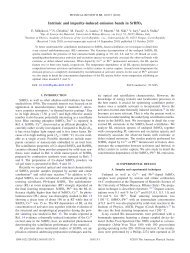
3.2 Sample characterization 39<br />
Figure 3.9: AFM tapping mode images <strong>of</strong> a 3 × 3 µm 2 region <strong>of</strong> the surface <strong>of</strong> a<br />
sample consisting <strong>of</strong> a <strong>rubrene</strong> thin film grown on top <strong>of</strong> a quatertiophene thin film.<br />
(a) Height image. (b) Phase contrast image collected at the same time as (a).<br />
order to minimize the tip-sample electrostatic interaction. The resulting<br />
voltage between the tip <strong>and</strong> the sample then is:<br />
∆V = ∆ϕ − Vdc + Vac sin(ωt) (3.3)<br />
where ∆ϕ is the work function difference (or contact potential difference)<br />
between the tip <strong>and</strong> the sample, Vdc is the DC potential applied to the tip<br />
<strong>and</strong> ω is the frequency <strong>of</strong> the applied Vac bias. If the tip-sample distance is<br />
smaller than the tip radius, then the tip-sample system can be considered as<br />
a parallel plate capacitor whose energy U is given by<br />
U = 1 2<br />
C∆V<br />
2<br />
where C is the capacitance <strong>of</strong> the tip-sample system.<br />
(3.4)<br />
The electrostatic force between the tip <strong>and</strong> the sample is then given by<br />
F = − ∂U<br />
∂z<br />
∂C<br />
= −1<br />
2 ∂z ∆V 2 = Fdc + Fω + F2ω<br />
where the three components <strong>of</strong> the force are<br />
Fdc = − 1<br />
<br />
∂C<br />
(∆ϕ − Vdc)<br />
2 ∂z<br />
2 +<br />
<br />
V 2<br />
ac<br />
2<br />
(3.5)<br />
(3.6)