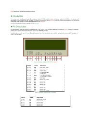
Comparison of CMOS Current Conveyor Circuits for Non-Foster ...
Comparison of CMOS Current Conveyor Circuits for Non-Foster ...
Comparison of CMOS Current Conveyor Circuits for Non-Foster ...

You also want an ePaper? Increase the reach of your titles
YUMPU automatically turns print PDFs into web optimized ePapers that Google loves.
<strong>Comparison</strong> <strong>of</strong> <strong>CMOS</strong> <strong>Current</strong> <strong>Conveyor</strong> <strong>Circuits</strong> <strong>for</strong><br />
<strong>Non</strong>-<strong>Foster</strong> Applications<br />
Varun S. Kshatri, John M. C. Covington III, Joshua W. Shehan, Thomas P. Weldon, and Ryan S. Adams<br />
Department <strong>of</strong> Electrical and Computer Engineering<br />
University <strong>of</strong> North Carolina at Charlotte<br />
Charlotte, NC, USA<br />
tpweldon@uncc.edu<br />
Abstract— <strong>Current</strong> conveyors are an important component<br />
<strong>for</strong> implementing non-<strong>Foster</strong> circuits such as negative capacitors<br />
and negative resistors. However, different topologies exist <strong>for</strong><br />
implementing negative capacitance using a current conveyor, and<br />
the per<strong>for</strong>mance <strong>of</strong> such topologies can vary greatly. There<strong>for</strong>e,<br />
this paper considers two competing realizations <strong>of</strong> negative<br />
capacitance using a current conveyor, where both circuits are<br />
designed <strong>for</strong> -5 pF in a 0.5 micron <strong>CMOS</strong> process. Simulation<br />
results are presented that show significant bandwidth differences<br />
<strong>for</strong> the two -5 pF designs, where one approach has more than<br />
twice the bandwidth <strong>of</strong> the second approach.<br />
Keywords—negative capacitance; negative impedance converter;<br />
<strong>CMOS</strong>; bandwidth; second generation current conveyor (CCII+).<br />
I. INTRODUCTION<br />
A current conveyor is a basic building block that has found<br />
wide application since its introduction in 1968 by Smith and<br />
Sedra [1] and the re<strong>for</strong>mulation in 1970 by Sedra and Smith<br />
[2]. <strong>Current</strong> conveyors have found use in current-mode and<br />
mixed-mode filter design, instrumentation and wideband<br />
amplifiers, and non-<strong>Foster</strong> circuits [3]-[5], [7]-[8]. Although<br />
current conveyors have been used <strong>for</strong> more than four decades,<br />
there is renewed interest in their use in a variety <strong>of</strong> analog<br />
signal processing tasks such as oscillators, controlled sources,<br />
impedance convertors, impedance inverters, gyrators, and<br />
various analog computation elements. The present paper<br />
compares two topologies <strong>of</strong> current conveyors <strong>for</strong> relative<br />
bandwidth per<strong>for</strong>mance in a 0.5 micron <strong>CMOS</strong> process <strong>for</strong><br />
non-<strong>Foster</strong> applications. In this, simulation results show<br />
marked differences in bandwidth as noted <strong>for</strong> other processes<br />
[6].<br />
There are several generations <strong>of</strong> current conveyors with<br />
different sets <strong>of</strong> equations describing current and voltage<br />
relationships at the terminals <strong>of</strong> the devices. In this paper,<br />
second-generation current conveyors (CCII) are considered <strong>for</strong><br />
the realization <strong>of</strong> negative capacitance using two different<br />
circuit topologies. Although the same current conveyor is used<br />
in both topologies, simulation results are given that show one<br />
approach has twice the bandwidth <strong>of</strong> the other.<br />
In the following section, the second-generation <strong>CMOS</strong><br />
current conveyor is described, and the two competing circuit<br />
topologies <strong>for</strong> negative capacitance are described. The<br />
This material is based upon work supported by the National Science<br />
Foundation under Grant No. ECCS-1101939.<br />
subsequent section describes the detailed design, layout, and<br />
simulation results <strong>for</strong> the proposed circuits. The simulation<br />
results demonstrate significant per<strong>for</strong>mance differences<br />
between the two competing topologies when compared <strong>for</strong> a<br />
nominal design goal <strong>of</strong> -5 pF.<br />
II. CIRCUIT ANALYSIS<br />
The CCII current conveyor to be investigated is based on a<br />
Sedra and Smith second-generation current conveyor [2], and<br />
is shown in Fig. 1. It is a three-port device with the following<br />
set <strong>of</strong> equations:<br />
! ! = ! ! , (1)<br />
! ! = 0 , (2)<br />
! ! = ! ! , (3)<br />
where vx and ix are the input voltage and current to the X<br />
terminal, vy and iy are the input voltage and current to the Y<br />
terminal, and vz and iz are the input voltage and current to the<br />
Z terminal <strong>of</strong> Fig. 1. The sign <strong>of</strong> the current iz in (3)<br />
determines the positive or negative type <strong>of</strong> second-generation<br />
current conveyor (CCII). As given in (3) above, and in the<br />
following discussion, a positive CCII device (CCII+) is used.<br />
The first negative capacitance circuit topology under<br />
consideration is shown in Fig. 2, where the Z terminal is<br />
connected to the Y terminal. The same point also serves as the<br />
input <strong>of</strong> the overall circuit, having input impedance Zin with<br />
respect to ground. A load impedance ZL is connected from<br />
terminal X to ground, and serves as the reference impedance<br />
that is to be inverted.<br />
Fig. 1. Basic CCII+ current conveyor voltages and currents.
Fig. 2. First negative capacitance circuit topology using a CCII+ current<br />
conveyor. Input impedance Zin is between terminal Y and ground, and<br />
load impedance ZL is between terminal X and ground, where Zin = -ZL.<br />
From the node at terminal X in Fig. 2,<br />
! ! = − !!<br />
! , (4)<br />
!!<br />
and since iz = ix from (3), and since vx = vy. from (1), then<br />
! ! = − !!<br />
! . (5)<br />
!!<br />
At the input terminal, Y, the input voltage vin = vy, and since<br />
iy = 0 from (2), summing currents at terminal Y yields iin = iz,<br />
and so (5) becomes<br />
! !" = − ! !"<br />
! , (6)<br />
!!<br />
and the input impedance Zin is<br />
! !" = ! !"<br />
= −!<br />
!<br />
! . (7)<br />
!"<br />
The second negative capacitance circuit topology under<br />
consideration is shown in Fig. 3, where the Z terminal <strong>of</strong> the<br />
CCII+ is connected to the Y terminal, and now the X terminal<br />
serves as the input terminal <strong>of</strong> the circuit having input<br />
impedance Zin with respect to ground. A load impedance ZL is<br />
Fig. 3. Second negative capacitance circuit topology using a CCII+ current<br />
conveyor. Input impedance Zin is between terminal X and ground, and<br />
load impedance ZL is between terminal Z and ground, where Zin = -ZL.<br />
Fig. 4. Detailed schematic <strong>of</strong> current conveyor circuit (CCII+).<br />
also connected from the Z terminal to ground, where ZL serves<br />
as the reference impedance to be inverted.<br />
For the circuit <strong>of</strong> Fig. 3, since iy = 0 from (2), then<br />
! ! = − !!<br />
! . (8)<br />
!!<br />
From (1) the input voltage vin = vx = vy = vz, and iz = iy from<br />
(3), so rearranging, (8) becomes<br />
! !" = !!<br />
=<br />
!!<br />
! !"<br />
= −!<br />
!<br />
! . (9)<br />
!"<br />
III. RESULTS<br />
The detailed schematic <strong>of</strong> the <strong>CMOS</strong> implementation <strong>of</strong> the<br />
CCII+ current conveyor is shown in Fig. 3, where all pMOS<br />
are 100×0.5 microns and all nMOS are 50×0.5 microns. The<br />
layout <strong>of</strong> the CCII+ <strong>of</strong> Fig. 4 in 0.5 micron <strong>CMOS</strong> is shown in<br />
Fig. 5, and the design is currently out <strong>for</strong> fabrication.<br />
Fig. 5. Layout <strong>of</strong> current conveyor (CCII+) circuit in 0.5 micron <strong>CMOS</strong>.
Fig. 6. Simulation results showing real part <strong>of</strong> Zin (solid blue) and<br />
imaginary part <strong>of</strong> Zin (dotted red) <strong>for</strong> a 5 pF capacitive load ZL <strong>for</strong> the<br />
circuit <strong>of</strong> Fig. 2.<br />
To compare the per<strong>for</strong>mance <strong>of</strong> the two topologies <strong>of</strong> Fig. 2<br />
and Fig. 3, the two designs were simuluated with a 5 pF load<br />
<strong>for</strong> ZL. In this case, both circuits then have an expected input<br />
impedance Zin corresponding to a -5 pF negative capacitance.<br />
The simulation results <strong>for</strong> Zin <strong>of</strong> the circuit in Fig. 2 are<br />
shown in Fig. 6, with the real part <strong>of</strong> Zin shown in solid blue<br />
and the imaginary part <strong>of</strong> Zin shown in dotted red. As is evident<br />
in Fig. 6, the imaginary part <strong>of</strong> the impedance follows the<br />
expected pr<strong>of</strong>ile <strong>of</strong> a negative capacitance, where the sign <strong>of</strong><br />
the reactance is inverted from that a <strong>of</strong> a positve capacitance.<br />
The simulation results <strong>for</strong> Zin <strong>of</strong> the circuit in Fig. 3 are shown<br />
in Fig. 7.<br />
The resulting capacitances at the inputs <strong>of</strong> the circuits <strong>of</strong><br />
Fig. 2 and Fig. 3 are shown in Fig. 8 and Fig. 9, respectively.<br />
As seen in the simulation results <strong>of</strong> Fig. 8 and Fig. 9, the<br />
capacitance values are near their expected values <strong>of</strong> -5 pF at<br />
low frequency, with corresponding low-frequency capacitances<br />
<strong>of</strong> -4.1 pF and -5.7 pF respectively. However, comparing the<br />
results <strong>of</strong> Fig. 8 and Fig. 9, the circuit <strong>of</strong> Fig. 3 has<br />
substantially larger bandwidth than the circuit <strong>of</strong> Fig. 2.<br />
Fig. 7. Simulation results showing real part <strong>of</strong> Zin (solid blue) and<br />
imaginary part <strong>of</strong> Zin (dotted red) <strong>for</strong> a 5 pF capacitive load ZL <strong>for</strong> the<br />
circuit <strong>of</strong> Fig. 3.<br />
Fig. 8. Simulation results showing input capacitance observed at Zin <strong>for</strong> a<br />
load capacitance ZL <strong>of</strong> 5 pF <strong>for</strong> the topology <strong>of</strong> Fig. 2 (computed<br />
capacitance values above the resonance near 300 MHz are anomalous due<br />
to zero crossing <strong>of</strong> Im(Z) ).<br />
Finally, as is typical with many non-<strong>Foster</strong> circuits, the<br />
two circuits were observed to be sensitive to the impedances<br />
<strong>of</strong> the signal sources used in the simulation. Although not<br />
evident in the results <strong>of</strong> Fig. 8 and Fig. 9, the circuit <strong>of</strong> Fig. 2<br />
used a source impedance <strong>of</strong> 50 ohms and the circuit <strong>of</strong> Fig. 3<br />
was tested with a 2500 ohm source impedance. To illustrate<br />
this, the circuit <strong>of</strong> Fig. 10 is a representative model <strong>of</strong> the<br />
input impedance <strong>of</strong> the circuit <strong>of</strong> Fig. 3 with impedance <strong>of</strong><br />
Fig. 7. In Fig. 10, Rp = -2500 Ω, Rs = 180 Ω, and C = -6 pF.<br />
The circuit <strong>of</strong> Fig. 10 approaches an impedance <strong>of</strong> Zin = 180<br />
Ω, at high frequency, just as the simulation <strong>of</strong> Fig. 7. At dc,<br />
the circuit <strong>of</strong> Fig. 10 approaches an impedance <strong>of</strong> Zin = -2320<br />
Ω, corresponding to the downward trajectory <strong>of</strong> Re(Z) seen at<br />
the lowest frequency <strong>of</strong> Fig. 7. Thus, a source impedance<br />
greater than 2320 ohms was used <strong>for</strong> the circuit <strong>of</strong> Fig. 3 to<br />
ensure stable simulations at low frequency [9].<br />
IV. CONCLUSION<br />
Two different circuit topologies <strong>for</strong> negative capacitance were<br />
simulated using second-generation <strong>CMOS</strong> current conveyors<br />
Fig. 9. Simulation results showing input capacitance observed at Zin <strong>for</strong> a<br />
load capacitance ZL <strong>of</strong> 5 pF <strong>for</strong> the topology <strong>of</strong> Fig. 3 (computed<br />
capacitance values above the resonance near 1000 MHz are anomalous).
Fig. 10. Circuit model <strong>for</strong> input impedance Zin <strong>of</strong> the topology <strong>of</strong> Fig.<br />
3 with impedance <strong>of</strong> Fig. 7.<br />
(CCII+). The analysis <strong>of</strong> the circuits, under simplifying<br />
assumptions, shows that the expected observed negative<br />
capacitances should approximately equal the negative <strong>of</strong> the<br />
load capacitances. The simulation results are in good<br />
agreement <strong>for</strong> the 5 pF external load, with observed negative<br />
capacitances <strong>of</strong> -4.1 pF and -5.7 pF at low frequency.<br />
However, one topology is observed to have more than twice<br />
the bandwidth <strong>of</strong> the other, even though the same <strong>CMOS</strong><br />
CCII+ is used in both cases. The only difference between the<br />
two cases is the configuration <strong>of</strong> the circuitry external to the<br />
CCII+.<br />
ACKNOWLEDGMENT<br />
This material is based upon work supported by the National<br />
Science Foundation under Grant No. ECCS-1101939.<br />
REFERENCES<br />
[1]. K. C. Smith and A. Sedra, “The current conveyor - A new circuit<br />
building block,” Proceedings <strong>of</strong> the IEEE, vol. 56, no.8, pp. 1368-<br />
1369, Aug. 1968.<br />
[2]. A. Sedra and K. C. Smith, “A second generation current conveyor<br />
and its applications,” IEEE Trans. on Circuit Theory, vol.17, no.1,<br />
pp. 132-134, Feb. 1970.<br />
[3]. M. T. Abuelma’atti and A. Bentrcia, “A novel mixed-mode CCIIbased<br />
filter,” Active and Passive Electronic Components, vol. 27,<br />
pp. 197-205, Dec. 2004.<br />
[4]. C. Galanis and I. Haritantis, “An improved current mode<br />
instrumentation amplifier,” Proceedings <strong>of</strong> the third IEEE<br />
international conference on Electronics, <strong>Circuits</strong> and System, vol.<br />
1, pp. 65-68, Oct. 1996.<br />
[5]. T. P. Weldon, K. Miehle, R. S. Adams and K. Daneshvar, "A<br />
wideband microwave double-negative metamaterial with non-<br />
<strong>Foster</strong> loading," 2012 Proceedings <strong>of</strong> IEEE SoutheastCon, pp. 1-5,<br />
15-18, Mar. 2012.<br />
[6]. J. Popovic, A. Pavasovic, and D. Vasiljevic, “Low-power High<br />
Bandwidth <strong>CMOS</strong> <strong>Current</strong> <strong>Conveyor</strong>,” PROC 21st International<br />
Conference on Microelectronics (MIEL’97), vol. 2, Yugoslavia,<br />
Sep. 1997.<br />
[7]. W. Surakampontorn, V. Riewruja, K. Kumwachara and K.<br />
Dejhan, “Accurate <strong>CMOS</strong>-based current conveyors,” IEEE Trans.<br />
Instvum. Meas., vol. 40, no. 4, pp. 699-702, Aug. 1991.<br />
[8]. A. S. Sedra, G.W. Roberts and F. Gohh, “The current conveyor:<br />
history, progress and new results,” IEE Proc. <strong>of</strong> ISCAS 1990, Vol.<br />
137, pp 78-87<br />
[9]. S. D. Stearns, “<strong>Non</strong>-<strong>Foster</strong> circuits and stability theory,” 2011<br />
IEEE International Symposium Antenas and Propagation<br />
(APSURSI), pp. 1942-1945, Jul. 2011.