Comparison of CMOS Current Conveyor Circuits for Non-Foster ...
Comparison of CMOS Current Conveyor Circuits for Non-Foster ...
Comparison of CMOS Current Conveyor Circuits for Non-Foster ...

You also want an ePaper? Increase the reach of your titles
YUMPU automatically turns print PDFs into web optimized ePapers that Google loves.
Fig. 2. First negative capacitance circuit topology using a CCII+ current<br />
conveyor. Input impedance Zin is between terminal Y and ground, and<br />
load impedance ZL is between terminal X and ground, where Zin = -ZL.<br />
From the node at terminal X in Fig. 2,<br />
! ! = − !!<br />
! , (4)<br />
!!<br />
and since iz = ix from (3), and since vx = vy. from (1), then<br />
! ! = − !!<br />
! . (5)<br />
!!<br />
At the input terminal, Y, the input voltage vin = vy, and since<br />
iy = 0 from (2), summing currents at terminal Y yields iin = iz,<br />
and so (5) becomes<br />
! !" = − ! !"<br />
! , (6)<br />
!!<br />
and the input impedance Zin is<br />
! !" = ! !"<br />
= −!<br />
!<br />
! . (7)<br />
!"<br />
The second negative capacitance circuit topology under<br />
consideration is shown in Fig. 3, where the Z terminal <strong>of</strong> the<br />
CCII+ is connected to the Y terminal, and now the X terminal<br />
serves as the input terminal <strong>of</strong> the circuit having input<br />
impedance Zin with respect to ground. A load impedance ZL is<br />
Fig. 3. Second negative capacitance circuit topology using a CCII+ current<br />
conveyor. Input impedance Zin is between terminal X and ground, and<br />
load impedance ZL is between terminal Z and ground, where Zin = -ZL.<br />
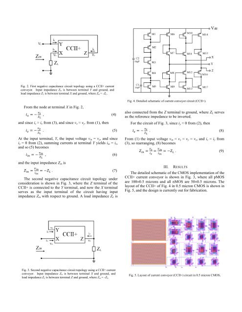
Fig. 4. Detailed schematic <strong>of</strong> current conveyor circuit (CCII+).<br />
also connected from the Z terminal to ground, where ZL serves<br />
as the reference impedance to be inverted.<br />
For the circuit <strong>of</strong> Fig. 3, since iy = 0 from (2), then<br />
! ! = − !!<br />
! . (8)<br />
!!<br />
From (1) the input voltage vin = vx = vy = vz, and iz = iy from<br />
(3), so rearranging, (8) becomes<br />
! !" = !!<br />
=<br />
!!<br />
! !"<br />
= −!<br />
!<br />
! . (9)<br />
!"<br />
III. RESULTS<br />
The detailed schematic <strong>of</strong> the <strong>CMOS</strong> implementation <strong>of</strong> the<br />
CCII+ current conveyor is shown in Fig. 3, where all pMOS<br />
are 100×0.5 microns and all nMOS are 50×0.5 microns. The<br />
layout <strong>of</strong> the CCII+ <strong>of</strong> Fig. 4 in 0.5 micron <strong>CMOS</strong> is shown in<br />
Fig. 5, and the design is currently out <strong>for</strong> fabrication.<br />
Fig. 5. Layout <strong>of</strong> current conveyor (CCII+) circuit in 0.5 micron <strong>CMOS</strong>.