Comparison of CMOS Current Conveyor Circuits for Non-Foster ...
Comparison of CMOS Current Conveyor Circuits for Non-Foster ...
Comparison of CMOS Current Conveyor Circuits for Non-Foster ...

Create successful ePaper yourself
Turn your PDF publications into a flip-book with our unique Google optimized e-Paper software.
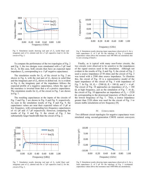
Fig. 6. Simulation results showing real part <strong>of</strong> Zin (solid blue) and<br />
imaginary part <strong>of</strong> Zin (dotted red) <strong>for</strong> a 5 pF capacitive load ZL <strong>for</strong> the<br />
circuit <strong>of</strong> Fig. 2.<br />
To compare the per<strong>for</strong>mance <strong>of</strong> the two topologies <strong>of</strong> Fig. 2<br />
and Fig. 3, the two designs were simuluated with a 5 pF load<br />
<strong>for</strong> ZL. In this case, both circuits then have an expected input<br />
impedance Zin corresponding to a -5 pF negative capacitance.<br />
The simulation results <strong>for</strong> Zin <strong>of</strong> the circuit in Fig. 2 are<br />
shown in Fig. 6, with the real part <strong>of</strong> Zin shown in solid blue<br />
and the imaginary part <strong>of</strong> Zin shown in dotted red. As is evident<br />
in Fig. 6, the imaginary part <strong>of</strong> the impedance follows the<br />
expected pr<strong>of</strong>ile <strong>of</strong> a negative capacitance, where the sign <strong>of</strong><br />
the reactance is inverted from that a <strong>of</strong> a positve capacitance.<br />
The simulation results <strong>for</strong> Zin <strong>of</strong> the circuit in Fig. 3 are shown<br />
in Fig. 7.<br />
The resulting capacitances at the inputs <strong>of</strong> the circuits <strong>of</strong><br />
Fig. 2 and Fig. 3 are shown in Fig. 8 and Fig. 9, respectively.<br />
As seen in the simulation results <strong>of</strong> Fig. 8 and Fig. 9, the<br />
capacitance values are near their expected values <strong>of</strong> -5 pF at<br />
low frequency, with corresponding low-frequency capacitances<br />
<strong>of</strong> -4.1 pF and -5.7 pF respectively. However, comparing the<br />
results <strong>of</strong> Fig. 8 and Fig. 9, the circuit <strong>of</strong> Fig. 3 has<br />
substantially larger bandwidth than the circuit <strong>of</strong> Fig. 2.<br />
Fig. 7. Simulation results showing real part <strong>of</strong> Zin (solid blue) and<br />
imaginary part <strong>of</strong> Zin (dotted red) <strong>for</strong> a 5 pF capacitive load ZL <strong>for</strong> the<br />
circuit <strong>of</strong> Fig. 3.<br />
Fig. 8. Simulation results showing input capacitance observed at Zin <strong>for</strong> a<br />
load capacitance ZL <strong>of</strong> 5 pF <strong>for</strong> the topology <strong>of</strong> Fig. 2 (computed<br />
capacitance values above the resonance near 300 MHz are anomalous due<br />
to zero crossing <strong>of</strong> Im(Z) ).<br />
Finally, as is typical with many non-<strong>Foster</strong> circuits, the<br />
two circuits were observed to be sensitive to the impedances<br />
<strong>of</strong> the signal sources used in the simulation. Although not<br />
evident in the results <strong>of</strong> Fig. 8 and Fig. 9, the circuit <strong>of</strong> Fig. 2<br />
used a source impedance <strong>of</strong> 50 ohms and the circuit <strong>of</strong> Fig. 3<br />
was tested with a 2500 ohm source impedance. To illustrate<br />
this, the circuit <strong>of</strong> Fig. 10 is a representative model <strong>of</strong> the<br />
input impedance <strong>of</strong> the circuit <strong>of</strong> Fig. 3 with impedance <strong>of</strong><br />
Fig. 7. In Fig. 10, Rp = -2500 Ω, Rs = 180 Ω, and C = -6 pF.<br />
The circuit <strong>of</strong> Fig. 10 approaches an impedance <strong>of</strong> Zin = 180<br />
Ω, at high frequency, just as the simulation <strong>of</strong> Fig. 7. At dc,<br />
the circuit <strong>of</strong> Fig. 10 approaches an impedance <strong>of</strong> Zin = -2320<br />
Ω, corresponding to the downward trajectory <strong>of</strong> Re(Z) seen at<br />
the lowest frequency <strong>of</strong> Fig. 7. Thus, a source impedance<br />
greater than 2320 ohms was used <strong>for</strong> the circuit <strong>of</strong> Fig. 3 to<br />
ensure stable simulations at low frequency [9].<br />
IV. CONCLUSION<br />
Two different circuit topologies <strong>for</strong> negative capacitance were<br />
simulated using second-generation <strong>CMOS</strong> current conveyors<br />
Fig. 9. Simulation results showing input capacitance observed at Zin <strong>for</strong> a<br />
load capacitance ZL <strong>of</strong> 5 pF <strong>for</strong> the topology <strong>of</strong> Fig. 3 (computed<br />
capacitance values above the resonance near 1000 MHz are anomalous).