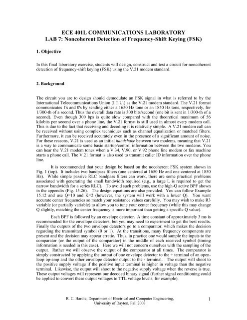
ECE 401L COMMUNICATIONS LABORATORY LAB 7 - University of ...
ECE 401L COMMUNICATIONS LABORATORY LAB 7 - University of ...
ECE 401L COMMUNICATIONS LABORATORY LAB 7 - University of ...

You also want an ePaper? Increase the reach of your titles
YUMPU automatically turns print PDFs into web optimized ePapers that Google loves.
<strong>ECE</strong> <strong>401L</strong> <strong>COMMUNICATIONS</strong> <strong><strong>LAB</strong>ORATORY</strong><br />
<strong>LAB</strong> 7: Noncoherent Detection <strong>of</strong> Frequency-Shift Keying (FSK)<br />
1. Objective<br />
In this final laboratory exercise, students will design, construct and test a circuit for noncoherent<br />
detection <strong>of</strong> frequency-shift keying (FSK) using the V.21 modem standard.<br />
2. Background<br />
The circuit you are to design should demodulate an FSK signal in what is referred to by the<br />
International Telecommunications Union (I.T.U.) as the V.21 modem standard. The V.21 format<br />
communicates 1's and 0's by sending either a 1650 Hz tone or an 1850 Hz tone, respectively, for<br />
1/300-th <strong>of</strong> a second. Thus the overall data rate is 300 bits/second (one bit is sent in 1/300-th <strong>of</strong> a<br />
second). Even though 300 bps is quite slow compared with the theoretical maximum <strong>of</strong> 56<br />
kilobits per second over a phone line, the V.21 format is still used in almost every modem call.<br />
This is due to the fact that receiving and decoding it is relatively simple. A V.21 modem call can<br />
be received without using complex techniques such as channel equalization or matched filters.<br />
Furthermore, it can be received accurately even in the presence <strong>of</strong> a significant amount <strong>of</strong> noise.<br />
For these reasons, V.21 is used as an initial handshake between two modems, meaning that V.21<br />
is a way to communicate some basic startup/control information between the two modems. You<br />
can hear the V.21 modem tones when a V.34, V.90, or V.92 phone line modem or fax machine<br />
starts a phone call. The V.21 format is also used to transmit caller ID information over the phone<br />
line.<br />
It is recommended that your design be based on the nocoherent FSK system shown in<br />
Fig. 1 (top). It includes two bandpass filters (one centered at 1650 Hz and one centered at 1850<br />
Hz). While simple passive RLC bandpass filters can work, there are some practical problems<br />
associated with generating the small bandwidth required (e.g., a large L is required to get the<br />
narrow bandwidth for a series RLC). To avoid such problems, use the high-Q active BPF shown<br />
in the appendix (Fig. 15.26). The design equations are also provided. You can follow Example<br />
15.12 and use Q=10 and K=2 (however, the system will work with a lower Q). You want<br />
accurate center frequencies so match your resistance values carefully. You may wish to make R3<br />
variable (or partially variable) to allow you to tune your center frequency (while this may change<br />
Q slightly, matching the center frequency is more important than getting a specific Q value).<br />
Each BPF is followed by an envelope detector. A time constant <strong>of</strong> approximately 3 ms is<br />
recommended for the envelope detectors, but you may need to experiment to get the best results.<br />
Finally the outputs <strong>of</strong> the two envelope detectors go to a comparator, which makes the decision<br />
regarding the transmitted symbol (0 or 1). At the transitions, many frequency components are<br />
present and the decision may appear erratic. Thus, in practice one would sample the inputs to the<br />
comparator (or the output <strong>of</strong> the comparator) in the middle <strong>of</strong> each received symbol (timing<br />
information is needed in this case). Here we will not concern ourselves with the sampling <strong>of</strong> the<br />
output. Rather we will observe the output <strong>of</strong> the comparator at all times. The comparator is<br />
simply constructed by applying the output <strong>of</strong> one envelope detector to the + terminal <strong>of</strong> an openloop<br />
op-amp and the other envelope detector output to the - terminal. The output will shoot to<br />
the positive supply voltage if the positive input terminal is higher in voltage than the negative<br />
terminal. Likewise, the output will shoot to the negative supply voltage when the reverse is true.<br />
These output voltages will represent our decoded binary signal (further signal conditioning could<br />
be applied to convert these output voltages to TTL voltage levels, for example).<br />
R. C. Hardie, Department <strong>of</strong> Electrical and Computer Engineering,<br />
<strong>University</strong> <strong>of</strong> Dayton, Fall 2003<br />
1
Figure 1: (top) Noncoherent demodulation <strong>of</strong> FSK (bottom) coherent demodulation <strong>of</strong> FSK.<br />
2. Prelab Assignment<br />
You should create a preliminary design for your FSK demodulator. Refinements to the design<br />
may be required as you construct and test your circuit. The design can be done as a lab group or<br />
individually. Prepare and submit a clear schematic for your design (at least one per lab group).<br />
Specify the key design equations used for each module in the design (i.e., BPF center frequency,<br />
BPF bandwidth, BPF Q-factor, time constant <strong>of</strong> envelope detectors, etc).<br />
3. Procedure<br />
3.1 BPF<br />
It is recommended that you construct your circuit in modules and test each module. In particular,<br />
construct each BPF and test the frequency response. Make sure the center frequency <strong>of</strong> each is<br />
very close to the desired frequency (note the two center frequencies are only 200 Hz apart). You<br />
may need to adjust your resistor values (possibly with a potentiometer for R3 to tune the BPF<br />
center frequencies). Once you are satisfied with the frequency response you observe, collect at<br />
least 10 magnitude frequency response measurements (output peak-to-peak voltage divided by<br />
input peak-to-peak voltage) around the center frequency <strong>of</strong> each BPF and generate a magnitude<br />
frequency response plot for each BPF. Do the BPFs behave as expected? It will be helpful to<br />
show the two frequency-response plots on the same axis in your report, since they work as a pair.<br />
Generate an FSK signal with the waveform generator. Be sure to correctly enter the two<br />
frequencies. Set the FSK rate (1/2 the bit rate) initially to 10 Hz to make it easier to test and<br />
debug your circuit. Inspect the output <strong>of</strong> one BPF on Channel 1 and the output <strong>of</strong> the other on<br />
Channel 2. One BPF output should have a large amplitude, while the other is small, and vice<br />
versa. If the BPFs appear to be working correctly, increase the FSK rate to 150 Hz (300 bits per<br />
second). Capture the outputs <strong>of</strong> the two BPFs simultaneously at this V.21 rate for your report.<br />
R. C. Hardie, Department <strong>of</strong> Electrical and Computer Engineering,<br />
<strong>University</strong> <strong>of</strong> Dayton, Fall 2003<br />
2
3.2 Envelope Detectors<br />
Next, construct the envelope detectors and test them. Keep in mind they must allow the signal to<br />
transition every 1/300-th <strong>of</strong> a second, but maintain a relatively constant output voltage during the<br />
duration <strong>of</strong> a bit (smoothing out the 1650 Hz or 1850 Hz signal coming in). We recommend<br />
starting with a time constant <strong>of</strong> approximately 3 ms (but again, you may need to tune it for<br />
optimum performance). Construct the envelope detectors and connect them to the outputs <strong>of</strong> the<br />
BPFs. Reduce the FSK rate back to 10 Hz signal with the waveform generator and inspect the<br />
output <strong>of</strong> one BPF on Channel 1 and the output <strong>of</strong> the corresponding envelope detector on<br />
Channel 2. The output <strong>of</strong> the envelope detector should look like a square wave and track the<br />
envelope <strong>of</strong> the BPF output (although some ripple may still be visible). Be sure your input<br />
voltage is sufficiently high for the envelope detector to operate correctly. Now increase the FSK<br />
rate to 150 Hz. Once you are satisfied with the envelope detectors, capture both envelope<br />
detector outputs simultaneously with an FSK rate <strong>of</strong> 150Hz for the report.<br />
3.3 Comparator<br />
Lastly, construct and test the comparator. Apply any periodic input to the comparator and look<br />
for the square-wave output that should result (remember the op-amp has no feedback path). Now<br />
connected the comparator to the rest <strong>of</strong> the circuit and try it! Start by using an FSK rate <strong>of</strong> 10Hz.<br />
Verify the output (it should be a square wave synced with the FSK signal). Increase your FSK<br />
rate to 150 Hz and capture the output. Demonstrate the operation <strong>of</strong> the complete circuit to the<br />
TA.<br />
3.4 The “Bit-rate Challenge” and Improvements (Optional)<br />
If time permits try to see how high a bit rate you can demodulate while maintaining a “clean”<br />
output (i.e., it stays high for one bit duration and stays low for the next with little or no<br />
oscillations over the duration <strong>of</strong> a bit). One thing that may improve the system’s performance is<br />
to add an RC LPF at the output <strong>of</strong> the comparator to remove any unwanted oscillations. Use a<br />
cut<strong>of</strong>f frequency above 2x the bit rate in Hertz (to pass the bit pulses) and below 1650 Hz (to<br />
suppress the oscillations, tune for optimum performance). Now, pass the output <strong>of</strong> the LPF<br />
through another comparator that compares with zero (ground the negative terminal). Does this<br />
output look cleaner? Let’s have a friendly competition to see who can get a clean output at the<br />
highest bit rate (the “bit-rate” challenge!).<br />
3.5 Audible Test<br />
Now let’s try to construct an “air” modem. Since the V.21 is designed for audible channels<br />
(phone lines), we can broadcast the FSK signal audibly and detect it with a microphone. Reduce<br />
the amplitude <strong>of</strong> the FSK signal and then connect a speaker to the waveform generator.<br />
Construct an amplifier with a gain <strong>of</strong> approximately 100 and connect a microphone to the input <strong>of</strong><br />
the amplifier and connect the output <strong>of</strong> the amplifier to the FSK demodulator circuit. Slowly<br />
increase the amplitude <strong>of</strong> the FSK signal using the waveform generator and place the microphone<br />
near the speaker. Now display the FSK signal on Channel 1 and the output <strong>of</strong> your FSK<br />
demodulator circuit on Channel 2. Does it work? If necessary, reduce the FSK rate. Capture an<br />
output waveform.<br />
R. C. Hardie, Department <strong>of</strong> Electrical and Computer Engineering,<br />
<strong>University</strong> <strong>of</strong> Dayton, Fall 2003<br />
3
3. Lab Write-up<br />
This lab write-up should be done in a formal report fashion. It should be done in Word and be<br />
formatted according to the guidelines provided on the <strong>ECE</strong><strong>401L</strong> website (under “formal report<br />
guidelines”). Provide information regarding the objective <strong>of</strong> the lab, show all theoretical design<br />
equations and calculations (use the equation editor), include sufficient experimental results to<br />
demonstrate the efficacy <strong>of</strong> your design, and provide meaningful conclusions and<br />
recommendations to possibly improve the design.<br />
Bonus: Provide us with an interesting scientific question and answer that we can use for future<br />
bonus questions (in the spirit <strong>of</strong> the previous bonus questions).<br />
APPENDIX: HIGH-Q ACTIVE BPF<br />
R. C. Hardie, Department <strong>of</strong> Electrical and Computer Engineering,<br />
<strong>University</strong> <strong>of</strong> Dayton, Fall 2003<br />
4
R. C. Hardie, Department <strong>of</strong> Electrical and Computer Engineering,<br />
<strong>University</strong> <strong>of</strong> Dayton, Fall 2003<br />
5
R. C. Hardie, Department <strong>of</strong> Electrical and Computer Engineering,<br />
<strong>University</strong> <strong>of</strong> Dayton, Fall 2003<br />
6
R. C. Hardie, Department <strong>of</strong> Electrical and Computer Engineering,<br />
<strong>University</strong> <strong>of</strong> Dayton, Fall 2003<br />
7
R. C. Hardie, Department <strong>of</strong> Electrical and Computer Engineering,<br />
<strong>University</strong> <strong>of</strong> Dayton, Fall 2003<br />
8