AM Modulation and Demodulation - University of Dayton : Homepages
AM Modulation and Demodulation - University of Dayton : Homepages
AM Modulation and Demodulation - University of Dayton : Homepages

You also want an ePaper? Increase the reach of your titles
YUMPU automatically turns print PDFs into web optimized ePapers that Google loves.
1. Objective<br />
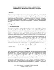
ECE 401L COMMUNICATIONS LABORATORY<br />
LAB 3: <strong>AM</strong> <strong>Modulation</strong> <strong>and</strong> <strong>Demodulation</strong><br />
Students will build <strong>and</strong> test a different type <strong>of</strong> amplitude modulation (<strong>AM</strong>) transmitter. The<br />
modulation will be accomplished by exploiting the nonlinear characteristics <strong>of</strong> a diode. The<br />
system will be tested by transmitting a signal to a commercial <strong>AM</strong> radio. Students will design,<br />
build <strong>and</strong> test the b<strong>and</strong>pass filter subsystem <strong>and</strong> the radio frequency (RF) amplifier stage.<br />
Students will also design, build <strong>and</strong> test an envelope detector for <strong>AM</strong> demodulation.<br />
2. Background<br />
2.1 <strong>Modulation</strong> using diode nonlinearity<br />
Amplitude modulation can be accomplished using a nonlinear element such as a forward biased<br />
diode near the turn-on voltage. The overall system to be implemented is shown in block diagram<br />
form in Figure 1. It is composed <strong>of</strong> a summer (Figure 2), a nonlinear circuit (Figure 3), a radio<br />
frequency (RF) amplifier, <strong>and</strong> a b<strong>and</strong>pass filter. The heart <strong>of</strong> the system is the nonlinear circuit<br />
shown in Figure 3. This circuit has an input-output function like that shown in Figure 4. This<br />
curve is governed by the voltage-current characteristic curve <strong>of</strong> the diode. Note that when the<br />
input voltage is in the 0.3V-0.5V range, the curve appears quadratic. We will exploit this to<br />
create a double-sideb<strong>and</strong> large-carrier (DSB-LC) <strong>AM</strong> signal.<br />
The input to the nonlinear circuit is the sum <strong>of</strong> a message signal, the carrier, <strong>and</strong> a DC bias<br />
voltage. Specifically this is given by<br />
The nonlinear circuit can be modeled with a polynomial as follows<br />
v1( t) = mt () + ct () + B.<br />
(1)<br />
v () t = cv () t + cv () t + cv () t + ...<br />
(2)<br />
2 3<br />
2 1 1 2 1 3 1<br />
Limiting this to a second order polynomial yields<br />
( ) ( ) 2<br />
v () t = c mt () + ct () + B + c mt () + ct () + B . (3)<br />
2 1 2<br />
This model seems reasonable, based on inspection <strong>of</strong> the input-output curve in Figure 4.<br />
Multiplying out the terms in (3) yields<br />
R. C. Hardie, Department <strong>of</strong> Electrical <strong>and</strong> Computer Engineering,<br />
<strong>University</strong> <strong>of</strong> <strong>Dayton</strong>, Fall 2003<br />
1
mt ()<br />
ct ()<br />
∑<br />
B<br />
1<br />
RF <strong>AM</strong>P BPF<br />
() v t 2 () v t 3 ()<br />
1 v t<br />
RF <strong>AM</strong>P BPF<br />
() v t 2 () v t 3 () v t<br />
Figure 1: <strong>AM</strong> modulator using nonlinear element<br />
( )<br />
( )<br />
v () t = 2 cmtct ()() + 2 cB+ c ct () (DSB-LC)<br />
2 2 2 1<br />
+ cB + cB<br />
2<br />
2 1<br />
+ + +<br />
2<br />
2 cB 2 c1 mt () cm 2 () t (baseb<strong>and</strong>)<br />
2<br />
cc 2 t<br />
(DC)<br />
+ ()<br />
(harmonic & DC)<br />
R. C. Hardie, Department <strong>of</strong> Electrical <strong>and</strong> Computer Engineering,<br />
<strong>University</strong> <strong>of</strong> <strong>Dayton</strong>, Fall 2003<br />
. (4)<br />
Note that we get some DC terms, baseb<strong>and</strong> terms, a harmonic term <strong>and</strong> the desired DSB-LC<br />
signal. The DSB-LC signal can be extracted by putting the signal through a b<strong>and</strong>pass filter.<br />
Assuming that the carrier is at a much higher frequency than the baseb<strong>and</strong> signal, a b<strong>and</strong>pass<br />
filter centered at the carrier frequency should be able to effectively eliminate the DC, baseb<strong>and</strong><br />
<strong>and</strong> harmonic terms. Neglecting the gain constant from the RF amplifier, this leaves us with the<br />
following signal<br />
( )<br />
v () t = 2 cmtct ()() + 2 cB+ c ct () . (5)<br />
3 2 2 1<br />
Note that for a sinusoidal carrier this represents a DSB-LC signal. The modulation index is given<br />
by<br />
2 c2|min{ mt ()}|<br />
m =<br />
. (6)<br />
2cB+<br />
c<br />
2 1<br />
Note that the modulation index is controlled in large part by the DC bias voltage <strong>and</strong> the message<br />
amplitude. We generally have little control over the polynomial parameters c 1 <strong>and</strong> c 2 .<br />
Because <strong>of</strong> the nature <strong>of</strong> the diode circuit, the voltage out <strong>of</strong> the nonlinear circuit is relatively<br />
small (typically less than 0.7V). Thus, an RF amplifier stage can be used to boost the signal<br />
prior to sending the signal to an antenna. As in the previous lab, we use a simple end-loaded wire<br />
antenna.<br />
2.2 <strong>Demodulation</strong> using envelope detection<br />
The envelope detector circuit is shown in Figure 5. It comprised <strong>of</strong> a diode followed by an RC<br />
circuit. When the input voltage is positive, the capacitor charges (i.e., step response). When the<br />
input goes negative, the diode becomes an open circuit <strong>and</strong> voltage on the capacitor exponentially<br />
2
decays (i.e., natural response) at a rate determined by the time constant ( τ = RC ). By choosing<br />
an appropriate value for the time constant, the voltage will closely follow the envelope <strong>of</strong> the<br />
modulated signal. The capacitor gets recharged by every peak but does not fall to zero between<br />
peaks because the time constant limits the decay. Thus, choosing the time constant <strong>of</strong> the RC<br />
circuit depends on the carrier frequency <strong>and</strong> message frequency. A rule <strong>of</strong> thumb is to use<br />
1/ f ≪τ = RC ≪ 1/ B,<br />
(7)<br />
c<br />
where f c is the carrier frequency in Hz <strong>and</strong> B is the b<strong>and</strong>width <strong>of</strong> the message signal. A lowpass<br />
filter can be employed after the envelope detector to smooth out ripple in the received signal.<br />
Figure 2: Summing amplifier circuit.<br />
Figure 3: Nonlinear circuit used for modulation.<br />
R. C. Hardie, Department <strong>of</strong> Electrical <strong>and</strong> Computer Engineering,<br />
<strong>University</strong> <strong>of</strong> <strong>Dayton</strong>, Fall 2003<br />
3
v2() t<br />
(V)<br />
0.3<br />
0.25<br />
0.2<br />
0.15<br />
0.1<br />
0.05<br />
Figure 4: Input/Output voltage relationship for nonlinear circuit (data from PSPICE with D1N4148<br />
diode <strong>and</strong> 1.8k Ohm resistor wi th no additional load).<br />
3. Prelab Assignment<br />
0<br />
0.2 0.3 0.4 0.5 0.6 0.7 0.8<br />
v1() t (V)<br />
Figure 5: Envelope detector for simple demodulation <strong>of</strong> DSB-LC signals.<br />
• Design a simple RLC b<strong>and</strong>pass filter centered at 600kHz with a 40kHz b<strong>and</strong>width (i.e.,<br />
attenuation < -3dB in a 40kHz passb<strong>and</strong>) using available component values. The lab has<br />
10uH, 47uH, <strong>and</strong> 100uH inductors. The available resistor values are shown in Table 1<br />
<strong>and</strong> the available capacitor values are shown in Table 2. Make sure you convert your<br />
design frequencies to radians/sec before using st<strong>and</strong>ard filter formulas. Verify your<br />
design with a PSPICE frequency sweep analysis.<br />
R. C. Hardie, Department <strong>of</strong> Electrical <strong>and</strong> Computer Engineering,<br />
<strong>University</strong> <strong>of</strong> <strong>Dayton</strong>, Fall 2003<br />
4
• Design a low-gain RF amplifier using a LF353 op-amp for the output stage. Keep in<br />
mind that the gain-b<strong>and</strong>width product for this op-amp is 4MHz. This is higher than the<br />
741 but it still limits our gain considerably for RF applications. For example, with a gain<br />
<strong>of</strong> 100, the op-amp circuit will only operate out to about 40kHz. Choose a suitable gain<br />
for operation at approximately 600kHz <strong>and</strong> design a non-inverting amplifier with this<br />
gain. Use available component values.<br />
• Design the envelope detector where ( B f )<br />
4. Procedure<br />
Use available component values.<br />
4.1 Nonlinear Circuit<br />
τ = 1/ + 1/ /2,<br />
B = 5 kHz <strong>and</strong> f = 600 kHz.<br />
Begin by constructing the nonlinear diode circuit shown in Figure 3. Let the input, v1( t ) , be a<br />
saw-tooth wave at 1kHz or higher. Set the peak-to-peak voltage to be 2V <strong>and</strong> set the DC <strong>of</strong>fset<br />
to +0.5V. Display the input on Channel 1 (X). Display the output, v2( t ) , on Channel 2 (Y). If<br />
the output looks as you would expect, according to (2), set the oscilloscope for XY mode (use the<br />
“Main/Delayed” button). Set the scales for approximately 200 mV/division on each input.<br />
Center the curve, which should look like that in Figure 4, <strong>and</strong> save a screen capture. Identify <strong>and</strong><br />
make note <strong>of</strong> the range <strong>of</strong> input voltages for which there is a nearly quadratic response. What is<br />
the approximate center <strong>of</strong> this input voltage range <strong>and</strong> what is its approximate extent?<br />
4.2 Summing Amplifier Subsystem<br />
To multiply two signals, we must add the two signals in question <strong>and</strong> apply the sum to the input<br />
<strong>of</strong> the nonlinear circuit. Since one <strong>of</strong> our signals is an RF carrier, we must construct our summer<br />
using a wide b<strong>and</strong>width operational amplifier (LF353, see datasheet attached). Construct the<br />
inverting summing circuit shown in Figure 2. Let the message, mt () , input be a 1kHz sinusoid<br />
from the WaveTek, with a peak-to-peak voltage <strong>of</strong> approximately 0.2V. Let the carrier be a 0.5V<br />
pp, 10kHz sinusoid, with a –0.4V DC <strong>of</strong>fset (note that this becomes +0.4V after the inverting<br />
summer). Apply the summed input to the nonlinear circuit. Display the summed signal on<br />
Channel 1 <strong>and</strong> the output <strong>of</strong> the nonlinear circuit on Channel 2. Use an external sync from the<br />
WaveTek so as to lock onto the message signal. Adjust the amplitudes <strong>and</strong> <strong>of</strong>fset as need to get<br />
the summed signal in the “sweet spot” <strong>of</strong> the nonlinear circuit, identified in Section 4.1. If you<br />
are satisfied with the result, save a screen capture <strong>and</strong> comment on what you observe. Try<br />
changing the message frequency <strong>and</strong> shape (square, sawtooth, etc) <strong>and</strong> observe the output.<br />
4.3 RF Amplifier<br />
To boost the output <strong>of</strong> the nonlinear circuit, construct the non-inverting low-gain RF amplifier<br />
that you designed in the pre-lab. This can be built using the second operational amplifier<br />
contained on the LF353 chip. Connect the output <strong>of</strong> the nonlinear circuit to the input <strong>of</strong> the RF<br />
amplifier <strong>and</strong> verify the operation <strong>of</strong> this circuit.<br />
R. C. Hardie, Department <strong>of</strong> Electrical <strong>and</strong> Computer Engineering,<br />
<strong>University</strong> <strong>of</strong> <strong>Dayton</strong>, Fall 2003<br />
c<br />
c<br />
5
4.4 <strong>AM</strong> Broadcasting<br />
Connect a length <strong>of</strong> wire to the output <strong>of</strong> the RF amplifier (i.e., an end-loaded wire antenna).<br />
Increase the carrier to approximately 600kHz <strong>and</strong> let the message to be a sinusoid at<br />
approximately 1kHz. Using the <strong>AM</strong> radio in the lab, tune in your signal by matching your<br />
carrier frequency <strong>and</strong> the receiver. Try transmitting different message frequencies <strong>and</strong><br />
waveforms. Comment on what you hear. Demonstrate your successful system for the TA.<br />
Build an inverting audio amplifier using a st<strong>and</strong>ard operational amplifier (i.e., dual LM1458 or<br />
single 741). Connect the microphone. Verify the output <strong>of</strong> the amplifier on the scope <strong>and</strong> select<br />
a gain (by changing the feedback resistor value) that yields roughly a 0.2V peak-to-peak output<br />
voltage when speaking normally (you want the same voltage levels that the WaveTek is<br />
producing). Connect the amplifier output in place <strong>of</strong> the WaveTek input <strong>and</strong> try transmitting your<br />
voice. How does the transmitter perform compared to the chopper modulator transmitter? Does<br />
it have more range, less range, or about the same?<br />
4.5 B<strong>and</strong> Pass Filter<br />
While not necessary for operation during the tests above, a b<strong>and</strong>pass filter would be required in<br />
any commercial <strong>AM</strong> transmitter to limit each station to approximately 10kHz (center frequencies<br />
ranging from 540kHz to 1600kHz). Construct the b<strong>and</strong>pass filter you designed in the pre-lab (do<br />
not incorporate into transmitter yet) <strong>and</strong> test it by applying a sinusoidal input <strong>and</strong> sweeping the<br />
frequency past the designed center frequency. Once you are satisfied with its operation,<br />
incorporate the filter into your system. If you wish to test transmission with the BPF in place,<br />
you need to move your antenna connection to the output <strong>of</strong> the BPF. Note that the passive BPF<br />
will cause some attenuation, even in the passb<strong>and</strong>, negatively impacting transmission power.<br />
Remove the microphone input from the summer <strong>and</strong> return to a 10kHz sinusoidal message signal<br />
from the WaveTek. Display the output <strong>of</strong> the RF amplifier (input to BPF) on Channel 1 <strong>and</strong> the<br />
output <strong>of</strong> the BPF on Channel 2. Save a screen capture showing these signals. Try different<br />
message signals <strong>and</strong> frequencies <strong>and</strong> observe the output. How does the time-domain output differ<br />
before <strong>and</strong> after the BPF? Explain the differences you observe. It may be helpful to refer to<br />
Equation (4).<br />
Use the FFT function to display the frequency spectrum <strong>of</strong> the signal before the BPF. Set the<br />
FFT for 2MSa/sec with a center frequency <strong>of</strong> 600kHz <strong>and</strong> a span <strong>of</strong> 500kHz. Try changing the<br />
message frequency, carrier frequency, message waveform, <strong>and</strong> observe the corresponding spectra.<br />
Try to underst<strong>and</strong> what you observe. Save a screen capture <strong>and</strong> explain the source <strong>of</strong> the major<br />
peaks in the spectrum that you capture. Be sure to capture the peak at the fundamental frequency<br />
<strong>of</strong> the carrier <strong>and</strong> the peaks from the message (the sideb<strong>and</strong> power). Next, observe the FFT <strong>of</strong> the<br />
signal after the BPF. Save a screen capture <strong>and</strong> explain what you observe.<br />
4.6 <strong>Demodulation</strong><br />
Construct the envelope detector in Figure 5 using the design values from the pre-lab. Test your<br />
detector with an <strong>AM</strong> signal from a laboratory signal generator. Initially use a 600kHz, 5V peakto-peak,<br />
sinusoidal carrier <strong>and</strong> 1kHz sinusoidal message (refer to Lab 1 if necessary). Observe<br />
the input <strong>AM</strong> signal on Channel 1 <strong>and</strong> your detector output on Channel 2. Use the external sync<br />
from the message signal generator. Save a screen capture illustrating the successful demodulation<br />
<strong>of</strong> an <strong>AM</strong> signal. Vary the modulation level <strong>and</strong> modulation waveform <strong>and</strong> observe the results.<br />
R. C. Hardie, Department <strong>of</strong> Electrical <strong>and</strong> Computer Engineering,<br />
<strong>University</strong> <strong>of</strong> <strong>Dayton</strong>, Fall 2003<br />
6
What happens when you over-modulate the carrier (modulation index > 1)? Vary the carrier<br />
frequency <strong>and</strong> observe the results? For what range <strong>of</strong> carrier frequencies does you detector<br />
appear to adequately demodulate a 1kHz sinusoidal message? What range <strong>of</strong> message<br />
frequencies does your detector adequately demodulate with a fixed 600kHz carrier?<br />
4.7 Computer Aided Analysis<br />
Calculate the frequency response <strong>of</strong> your BPF by h<strong>and</strong> <strong>and</strong> plot the magnitude <strong>and</strong> phase<br />
frequency response with MATLAB. Use units <strong>of</strong> dB for the gain (magnitude frequency<br />
response), <strong>and</strong> let the horizontal axis be frequency in Hz plotted on a log axis (i.e., use<br />
semilogx(.)). Using the equation editor in Word, include a few steps <strong>and</strong> the final result <strong>of</strong> your<br />
frequency response analysis in your report. What is the theoretical attenuation in dB at the<br />
carrier? What is the theoretical attenuation in dB 10kHz from the carrier?<br />
Analyze the nonlinear diode circuit in Figure 3. Insert a DC voltage source in PSPICE <strong>and</strong><br />
perform a DC sweep analysis, plotting the output over the resistor. The resulting plot should look<br />
like Figure 4. Use diode model D1N4148. Include the PSPICE plot <strong>and</strong> schematic in your writeup.<br />
5. Lab Write-up<br />
Create a Word document organized according the numbered procedure sections (Sections 4.1-<br />
4.7). Provide screen captures with detailed descriptions <strong>and</strong> answers to the questions posed in the<br />
lab next to the appropriate procedure section.<br />
Bonus Question: In the 1700’s a major scientific problem <strong>of</strong> the day was how to determine the<br />
longitude <strong>of</strong> a vessel at sea. Latitude, you see, can be determined by measuring the angle <strong>of</strong> the<br />
sun to the horizon at it highest point in the day. Longitude was not so simple in those days. Who<br />
is credited with solving this problem <strong>and</strong> how was it solved?<br />
R. C. Hardie, Department <strong>of</strong> Electrical <strong>and</strong> Computer Engineering,<br />
<strong>University</strong> <strong>of</strong> <strong>Dayton</strong>, Fall 2003<br />
7
Table 1: Resistor values available in the lab<br />
4.7 5.1 5.6 6.2 6.8 7.5 8.2 9.1<br />
10 12 15 18 20 22 24 27<br />
30 33 36 39 43 47 51 56<br />
62 68 75 82 91 100 120 150<br />
180 200 220 240 270 300 330 360<br />
390 430 470 510 560 620 680 750<br />
820 910 1k 1.2k 1.5k 1.8k 2k 2.2k<br />
2.4k 2.7k 3k 3.3k 3.6k 3.9k 4.3k 4.7k<br />
5.1k 6.2k 6.8k 7.5 8.2k 9.1k 10k 12k<br />
15k 18k 20k 22k 24k 27k 30k 33k<br />
36k 39k 43k 47k 51k 56k 62k 68k<br />
75k 82k 91k 100k 120k 150k 180k 200k<br />
220k 240k 270k 300k 330k 360k 390k 430k<br />
470k 510k 560k 620k 680k 750k 820k 910k<br />
1M 1.2M 1.5M 1.8M 2M 2.2M 2.4M 2.7M<br />
Table 2: Capacitor values available in the lab.<br />
10 pF 0.0022 uF 0.47 uF 470 uF<br />
15 pF 0.0033 uF 0.68 uF 1000 uF<br />
22 pF 0.0047 uF 1 uF 2200 uF<br />
33 pF 0.0068 uF 2.2 uF<br />
47 pF 0.01 uF 3.3 uF<br />
68 pF 0.015 uF 4.7 uF<br />
100 pF 0.1 uF 6.8 uF<br />
150 pF 0.15 uF 10 uF<br />
220 pF 0.047 uF 22 uF<br />
330 pF 0.061 uF 33 uF<br />
470 pF 0.022 uF 47 uF<br />
680 pF 0.033 uF 100 uF<br />
0.001 uF 0.22 uF 220 uF<br />
0.0015 uF 0.33 uF<br />
R. C. Hardie, Department <strong>of</strong> Electrical <strong>and</strong> Computer Engineering,<br />
<strong>University</strong> <strong>of</strong> <strong>Dayton</strong>, Fall 2003<br />
8