

Design of De-Emphasis and Equalization Circuits for Gigabit Serial ...
Design of De-Emphasis and Equalization Circuits for Gigabit Serial ...
Design of De-Emphasis and Equalization Circuits for Gigabit Serial ...

Create successful ePaper yourself
Turn your PDF publications into a flip-book with our unique Google optimized e-Paper software.
Memory<br />
Bridge<br />
FB-DIMM Configurations<br />
Read Data<br />
(Primary North)<br />
14<br />
10<br />
Write Data<br />
(Primary South)<br />
DRAM<br />
DRAM<br />
DRAM<br />
DRAM<br />
AMB<br />
DRAM<br />
DRAM<br />
DRAM<br />
DRAM<br />
Secondary<br />
North<br />
Secondary<br />
South<br />
DRAM<br />
DRAM<br />
DRAM<br />
DRAM<br />
AMB<br />
DRAM<br />
DRAM<br />
DRAM<br />
DRAM<br />
*Third party marks <strong>and</strong> br<strong>and</strong>s are the property <strong>of</strong> their respective owners<br />
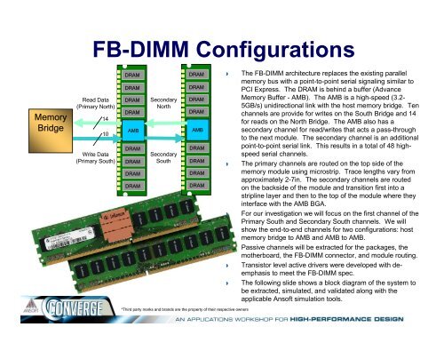
� The FB-DIMM architecture replaces the existing parallel<br />
memory bus with a point-to-point serial signaling similar to<br />
PCI Express. The DRAM is behind a buffer (Advance<br />
Memory Buffer - AMB). The AMB is a high-speed (3.2-<br />
5GB/s) unidirectional link with the host memory bridge. Ten<br />
channels are provide <strong>for</strong> writes on the South Bridge <strong>and</strong> 14<br />
<strong>for</strong> reads on the North Bridge. The AMB also has a<br />
secondary channel <strong>for</strong> read/writes that acts a pass-through<br />
to the next module. The secondary channel is an additional<br />
point-to-point serial link. This results in a total <strong>of</strong> 48 highspeed<br />
serial channels.<br />
� The primary channels are routed on the top side <strong>of</strong> the<br />
memory module using microstrip. Trace lengths vary from<br />
approximately 2-7in. The secondary channels are routed<br />
on the backside <strong>of</strong> the module <strong>and</strong> transition first into a<br />
stripline layer <strong>and</strong> then to the top <strong>of</strong> the module where they<br />
interface with the AMB BGA.<br />
� For our investigation we will focus on the first channel <strong>of</strong> the<br />
Primary South <strong>and</strong> Secondary South channels. We will<br />
show the end-to-end channels <strong>for</strong> two configurations: host<br />
memory bridge to AMB <strong>and</strong> AMB to AMB.<br />
� Passive channels will be extracted <strong>for</strong> the packages, the<br />
motherboard, the FB-DIMM connector, <strong>and</strong> module routing.<br />
� Transistor level active drivers were developed with deemphasis<br />
to meet the FB-DIMM spec.<br />
� The following slide shows a block diagram <strong>of</strong> the system to<br />
be extracted, simulated, <strong>and</strong> validated along with the<br />
applicable Ans<strong>of</strong>t simulation tools.


