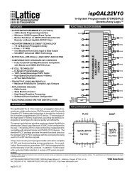
Beginner's Guide to ispLSI and pLSI Using pDS Software
Beginner's Guide to ispLSI and pLSI Using pDS Software
Beginner's Guide to ispLSI and pLSI Using pDS Software

You also want an ePaper? Increase the reach of your titles
YUMPU automatically turns print PDFs into web optimized ePapers that Google loves.
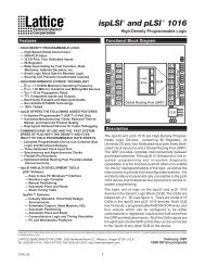
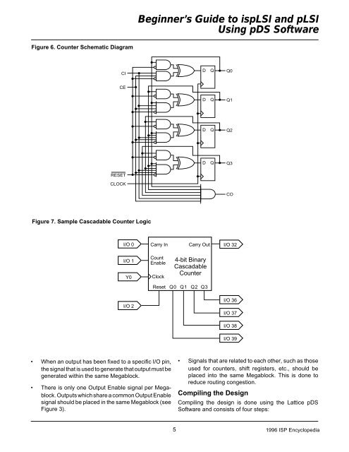
Figure 6. Counter Schematic Diagram<br />
CI<br />
CE<br />
RESET<br />
CLOCK<br />
Figure 7. Sample Cascadable Counter Logic<br />
Beginner’s <strong>Guide</strong> <strong>to</strong> <strong>is<strong>pLSI</strong></strong> <strong>and</strong> <strong>pLSI</strong><br />
<strong>Using</strong> <strong>pDS</strong> <strong>Software</strong><br />
D Q<br />
D Q<br />
D Q<br />
D Q<br />
Q0<br />
Q1<br />
Q2<br />
Q3<br />
CO<br />
I/O 0 Carry In Carry Out I/O 32<br />
I/O 1<br />
Y0<br />
I/O 2<br />
Count<br />
Enable<br />
Clock<br />
Reset<br />
• When an output has been fixed <strong>to</strong> a specific I/O pin,<br />
the signal that is used <strong>to</strong> generate that output must be<br />
generated within the same Megablock.<br />
• There is only one Output Enable signal per Megablock.<br />
Outputs which share a common Output Enable<br />
signal should be placed in the same Megablock (see<br />
Figure 3).<br />
4-bit Binary<br />
Cascadable<br />
Counter<br />
Q0 Q1 Q2 Q3<br />
I/O 36<br />
I/O 37<br />
I/O 38<br />
I/O 39<br />
• Signals that are related <strong>to</strong> each other, such as those<br />
used for counters, shift registers, etc., should be<br />
placed in<strong>to</strong> the same Megablock. This is done <strong>to</strong><br />
reduce routing congestion.<br />
Compiling the Design<br />
Compiling the design is done using the Lattice <strong>pDS</strong><br />
<strong>Software</strong> <strong>and</strong> consists of four steps:<br />
5 1996 ISP Encyclopedia