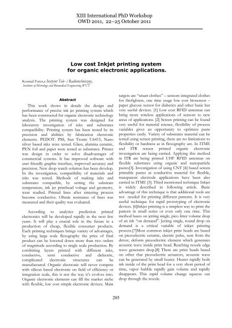
Low Cost Inkjet printing System For Organic Electronic
Low Cost Inkjet printing System For Organic Electronic
Low Cost Inkjet printing System For Organic Electronic

Create successful ePaper yourself
Turn your PDF publications into a flip-book with our unique Google optimized e-Paper software.
Konrad Futer,a Instytut Tele- i Radiotechniczny,<br />
Institute of Metrology and Biomedical Engineering WUT<br />
<strong>Low</strong> cost <strong>Inkjet</strong> <strong>printing</strong> system<br />
for organic electronic applications.<br />
Abstract<br />
This work shows in details the design and<br />
performance of precise ink jet <strong>printing</strong> system which<br />
has been constructed for organic electronic technology<br />
analysis. The <strong>printing</strong> system was designed for<br />
laboratory investigation of inks and substrates<br />
compatibility. Printing system has been tested by its<br />
precision and abilities by fabrication electronic<br />
elements. PEDOT: PSS, Sun Tronic U6415, Nano<br />
silver based inks were tested. Glass, alumina ceramic,<br />
PEN foil and paper were tested as substrates. Printer<br />
was design in order to solve disadvantages of<br />
commercial systems. It has improved software with<br />
user friendly graphic interface, improved accuracy and<br />
precision. New drop watch solution has been develop.<br />
In the investigation, compatibility of materials and<br />
inks was tested. Methods of making inks and<br />
substrates compatible, by setting the substrate<br />
temperature, ink jet printhead voltage and geometry,<br />
were studied. Printed lines after sintering process<br />
become conductive. Ohmic resistance of lines was<br />
measured and their quality was evaluated.<br />
According to analytics prediction printed<br />
electronics will be developed rapidly in the next few<br />
years. It will play a crucial role in the future in a<br />
production of cheap, flexible consumer products.<br />
Each <strong>printing</strong> techniques brings variety of advantages,<br />
by using large scale flexography the price of final<br />
product can be lowered down more than two orders<br />
of magnitude according to single scale production. By<br />
combining layers printed with different inks,<br />
conductive, semi conductive and dielectric,<br />
complicated electronic structures can be<br />
manufactured. <strong>Organic</strong> electronic will never compete<br />
with silicon based electronic on field of efficiency or<br />
integration scale, this is not the way it’s evolves into.<br />
<strong>Organic</strong> electronic elements can fill the market niche<br />
with flexible, low cost simple electronic devices. Main<br />
XIII International PhD Workshop<br />
OWD 2011, 22–25 October 2011<br />
205<br />
targets are “smart clothes” – sensors integrated clothes<br />
for firefighters, one time usage low cost biosensor –<br />
paper glucose sensor for diabetics and other basic but<br />
very useful devices. [1] <strong>Low</strong> cost RFID antennas can<br />
bring more wireless applications of sensors to new<br />
areas of applications. [2] Screen <strong>printing</strong> can be found<br />
very useful for material science, flexibility of process<br />
variables gives an opportunity to optimize paste<br />
properties easily. Variety of substrates material can be<br />
tested using screen <strong>printing</strong>, there are no limitations to<br />
flexibility or hardness as in flexography are. In ITME<br />
and ITR screen printed organic electronic<br />
investigation are being carried. Applying this method<br />
in ITR are being printed UHF RFID antennas on<br />
flexible substrates using organic and nanoparticle<br />
pastes[3]. Investigation of using CNT [4] based screen<br />
printable pastes as conductive material for flexible,<br />
transparent electrode applications have been also<br />
carried in ITME [5]. Third mentioned technique <strong>Inkjet</strong><br />
is widely described in following article. Basic<br />
advantage of this technique is that additional tools are<br />
not needed for <strong>printing</strong> different patterns. It is very<br />
useful technique for rapid prototyping of electronic<br />
devices. [6]<strong>Inkjet</strong> <strong>printing</strong> is a simplest way to print the<br />
pattern in small series or even only one time. This<br />
method bases on jetting single, pico litter volume drop<br />
of an ink “on demand”. Jetting single, round drop on<br />
demand is a critical variable of inkjet <strong>printing</strong><br />
process.[7]Most common inkjet print heads are based<br />
on piezoelectric ceramic, electric pulse, sent from the<br />
driver, deform piezoelectric element which generates<br />
acoustic wave inside print head. Reaching nozzle edge<br />
wave generates drop.[8] There are print heads based<br />
on other that piezoelectric actuators, acoustic wave<br />
can be generated by small heater. Heater rapidly boils<br />
ink inside of the print head for a very short period of<br />
time, vapor bubble rapidly gain volume and rapidly<br />
disappears. This rapid volume change squeeze out<br />
drop through the nozzle.
1. The design of <strong>Inkjet</strong> printer<br />
In this paper the design of piezoelectric print head<br />
based inkjet printer is described. It has been designed<br />
and built in Tele & Radio Research Institute (ITR). It<br />
is a small and low cost inkjet printer. The issue was to<br />
design flexible, low cost <strong>printing</strong> system to support<br />
material science investigation, technology optimization<br />
and new technology development. New <strong>printing</strong><br />
system should have <strong>printing</strong> abilities no lower than<br />
commercial printers and low cost couldn’t be an<br />
excuse. Commercial available <strong>printing</strong> systems has<br />
already been found inaccurate for some task realized<br />
in R&D units or in small laboratories. Those<br />
disadvantages, commonly described by the users were<br />
supposed to be removed from new designed <strong>printing</strong><br />
system. Built <strong>printing</strong> system, is based on MicroDrop,<br />
piezoceramic PZT print head system [9]. This specific<br />
system gives the highest spectrum of compatible inks.<br />
It is possible to use inks with pH in the range 1-12,<br />
viscosity 1-12 cPs. Nozzle diameters in this printer are<br />
50 µm and 100 µm, drop volume is in range from 35<br />
pl to 85 pl. Printhead has a heater, build in, that<br />
allows to heat up ink inside of the nozzle up to 100˚C.<br />
Printhead is controlled by attached driver unit.<br />
Generated electric pulse deforms piezoelectric<br />
actuator inside of the printhead. Operator controls the<br />
right pulse shape to get single “drop on demand”<br />
(DoD). Amplitude, length and delay of the pulse can<br />
be also set according to optimize drop shape.<br />
Amplitude can be set in range 0-250 V, length from 10<br />
– 300 ms, and delay from 1000 to 9999 µs. Control<br />
unit generates strobe signal for the strobe light. This<br />
gives the ability to observe drops in still – “frozen”<br />
position using simple CCD camera. This system is also<br />
called “Drop Watcher”. Delay of the strobe light<br />
signal can be adjust to freeze the right moment of the<br />
drop forming process. Commercial drop watch<br />
systems does not allow to freeze the picture<br />
Therefore, adjusting and optimization is less accurate<br />
then. Drop forming sequence taken by the strobe light<br />
CCD camera in different time delays is shown in Fig.<br />
1.<br />
Fig. 1. Drop forming sequence of PEDOT:PSS taken by<br />
the CCD camera. Time offset was 20µs, 30µs, 40µs.<br />
206<br />
2. Printing tests<br />
Printer abilities has been tested by <strong>printing</strong> patterns<br />
on most use substrates and by using variety of inks. To<br />
test precision and accuracy specific pattern was<br />
designs. An array of single dots, dot lines, horizontal<br />
and vertical. <strong>For</strong> system tests nano silver based ink was<br />
used, this ink is a commercial ink provide by<br />
Amepox[14]. Dot spacing was 0,15 mm, dot diameter<br />
100 µm. Printhead impulse was set to 110 V and 50<br />
µs. Substrate temperature was 65 ˚C. As a substrate<br />
glass was used. 10 exact patterns has been printed.<br />
Specimen were measured by using optical microscopy<br />
(see fig. 4). Diameter, spacing and position of each dot<br />
was measured and analyzed. Dots diameter was 100<br />
µm ± 4 µm, horizontal spacing 150 µm ± 2 µm,<br />
vertical spacing 150 µm ± 4 µm, position error 5 µm<br />
(as a distance from theoretic position to printed dot<br />
center), shape error 11 µm (as o standard deviations<br />
from ideal round shape).(Fig.2.)<br />
Fig. 2. Printed test pattern and shape precision.<br />
Shape precision and jetting accuracy was also<br />
investigated. As a substrate for this test, glass was<br />
used. Single drop was jetted one more time on the<br />
printed pattern. As it can be seen, dots from the<br />
second layer are deposited precise on centers of first<br />
layers dots. This proves very high <strong>printing</strong> precision.<br />
Second layer dots exhibit smaller shape error, less than<br />
3µm from model circular shape. However second layer<br />
dots have smaller diameter, the average diameter is 92<br />
µm. This is caused by different surface tension on<br />
clean substrate surface and printed dots surface.<br />
3. Line <strong>printing</strong> investigation<br />
Line <strong>printing</strong> ability was investigated. Using built<br />
<strong>printing</strong> system conductive lines were printed on<br />
ceramic substrate. As ink, nano silver based ink was<br />
used. Line <strong>printing</strong> tests were divided into four<br />
categories by quantity of layers. Lines were printed on<br />
substrate heated to four temperatures, 40°C, 60°C,<br />
80°C, 100°C. The issue was to find optimal parameters<br />
for <strong>printing</strong> conductive lines using nano silver based<br />
ink. Results of this test can be seen in tab. 1.
layers<br />
/tem<br />
p˚C<br />
40<br />
60<br />
80<br />
100<br />
1 2 3 4<br />
Table 1. Different substrate temperature and layers<br />
quantity <strong>printing</strong> results.<br />
Blur edges of prints are caused by the structure of<br />
ceramic substrate. First layer of ink soaked in the<br />
porous substrate and deform the edge. Second layer of<br />
ink forms a line, solvents evaporates fast enough, to<br />
prevent dots from spilling on the first layer. Different<br />
line structure, width and morphology can be achieved<br />
by using different combination of parameters. Due to<br />
the test, best results can be obtained by <strong>printing</strong> on<br />
ceramic substrate heated to 80 °C with three layers. All<br />
printed patterns were sintered in 350 °C for one hour.<br />
In this process organic ink ingredients evaporates, and<br />
lines became conductive. After sintering resistance of<br />
lines was measured. The lowest resistance has lines<br />
printed on substrate heated to 60 °C with four layers.<br />
Resistance of this line is 0,063 Ω, lines with five layers<br />
and more, has higher resistance. It is caused by surface<br />
cracks, lines with four layers and more has long, wide<br />
surface cracks. Resistance value for line with five<br />
layers is 0,083 Ω, six 0,097 Ω . (see fig. 3).<br />
Figure 3. Surface cracks on line printed on substrate<br />
heated to 60 °C with five layers. Sintered in 350 °C for<br />
one hour.<br />
Lines after sintering process can be seen in table 2.<br />
The “Coffee Ring” effect is strongly present. With<br />
line with three layers “Stack Coins” effect is observed.<br />
<strong>For</strong> four layer line none of these effects is present, but<br />
207<br />
“Halo” effect shows up. Halo effect is caused by<br />
porous structure of surface of alumina ceramic<br />
substrate that was used in this experiment.<br />
Layers 2 3 4<br />
Resistance 1,29 Ω 0,85 Ω 0,06 Ω<br />
Tab. 2. Printed conductive lines, after sintering by firing<br />
in 350 °C for one hour.<br />
4. Conclusions<br />
Achieved results show, that precise inkjet <strong>printing</strong><br />
system for organic electronic has been build. The<br />
advantage of this system is that it is low budget.<br />
Parameters of the new built system meet the<br />
commercial <strong>Inkjet</strong> <strong>printing</strong> systems, but it has been<br />
reached with ten times smaller budget. Developed new<br />
software makes pattern design easer for user, and<br />
graphic interface is more clear and friendly. Accuracy<br />
of the system was improved by using optimized<br />
maximum speed calculation algorithm. Printing<br />
precision of the printer is lower than 5µm and dot<br />
shape precision is not higher than 4µm. 100 µm ±5<br />
µm lines can be printed using this system, this meets<br />
most requirements for manufacturing simple<br />
electronic devices. Moreover substrate stage design<br />
gives higher standard of temperature stability. It<br />
improves heat transfer and even distribution on<br />
substrate surface for low heat conductive materials like<br />
ceramic or paper. New drop watch solution adopted in<br />
this system uses CCD camera directed at printhead<br />
nozzle, makes drops observation during <strong>printing</strong><br />
possible. This gives drops control feedback while<br />
<strong>printing</strong> process available. All these features sums up<br />
in high flexibility of <strong>printing</strong> system which opens new<br />
areas of possible usage of inkjet printers in electronic<br />
industry. Printed nano silver lines become conductive<br />
after sintering process. Sintering was executed by<br />
firing specimens in 350 °C for one hour. It is planned<br />
to investigate resistance sintering, as low temperature<br />
process, ready to print conductive lines on substrates<br />
fragile for high temperature firing. Printed conductive<br />
lines after firing have resistance 0,063 Ω. This values<br />
and precision makes this system ready for <strong>printing</strong>
Radio Frequency Identification antennas, sensors,<br />
precise MEMS devices, conductive lines and pads or<br />
transistor electrodes. It is planned to manufacture<br />
organic electronic circuits using this system, OFET<br />
(<strong>Organic</strong> Field Effect Transistor) based logic<br />
structures and OLED / PLED screens. <strong>System</strong> has<br />
now entered the final test stage were its abilities will be<br />
investigated in small scale production line. It is ready<br />
to fabricate elements on semi commercial scale, and<br />
new materials for new applications are being<br />
developed.<br />
References<br />
[1]. M.Sibinski, M.Jakubowska, M.Sloma „Flexible<br />
Temperature Sensors on Fibers” Sensors 2010,<br />
10(9), 7934-7946<br />
[2]. White Paper “OE-A Roadmap for <strong>Organic</strong> and<br />
Printed <strong>Electronic</strong>s”.<strong>Organic</strong> <strong>Electronic</strong><br />
Association, 2009,<br />
[3]. K. Janeczek, A. Młożniak, G. Kozioł, A. Araźna,<br />
M. Jakubowska, P. Bajurko, „Screen printed UHF<br />
antennas on flexible substrates”, Proceeding SPIE<br />
7745, 77451B (2010)<br />
[4]. M.Słoma M., Jakubowska M., Młożniak A.,<br />
„Multiwalled carbon nanotubes deposition in thick<br />
film silver conductor”, Proc. of SPIE Volume<br />
6937, 2007.<br />
[5]. Ptak J., Cież M., Zaraska K., Słoma M.,<br />
Jakubowska M., “A comparison of electrooptical<br />
characteristics of the electroluminescent lamps<br />
with transparent electrodes based on ITO and<br />
CNT”, Large-area <strong>Organic</strong> and Printed <strong>Electronic</strong>s<br />
Convention, June 23-25, 2009<br />
[6]. J. Sitek, K. Futera, K. Janeczek, K. Bukat, W.<br />
Stęplewski, M.Koscielski, M. Jakubowska,<br />
Investigation of inkjet technology forprinted<br />
organic electronics, Elektronika LII Nr 3/2011, s.<br />
112,<br />
[7]. M.M.Mohebi, J.R.G.Evans “A Drop-on-Demand<br />
Ink-Jet Printer for Combinatorial Libraries and<br />
Functionally Graded Ceramics“2002<br />
[8]. H.Wijshoff „The dynamics of the piezo inkjet<br />
printhead operation”, Physics Reports 2010<br />
[9]. Producer datasheet www.Microdrop.de.<br />
[10]. Thorlabs GmbH www.thorlabs.de – Motorized 2”<br />
LNR datasheet.<br />
[11]. Toshiba-Teli Corporation WWW.toshiba-teli.com<br />
prpduces datasheet.<br />
[12]. J Choi, J Yamaguchi, S Morales, Ro Horowitz, Y<br />
Zhao and A Majumdar,“Design and control of a<br />
thermal stabilizing system for a MEMS<br />
optomechanical uncooled infrared imaging camera<br />
“; 2003 Elsevier Science<br />
208<br />
[13]. FLIR SC645 data WWW.flir.com/themrmography<br />
[14]. Nanosilver ink datasheet http://www.amepoxmc.com<br />
Authors:<br />
Konrad FUTERA 1,2<br />
1Instytut Tele- i Radiotechniczny<br />
ul. Ratuszowa 11, 03-450<br />
Warszawa, 22 619 22 41,<br />
Konrad.futera@itr.org.pl<br />
2 Institute of Metrology and<br />
Biomedical Engineering<br />
Warsaw University of Technology<br />
ul. Św. Andrzeja Boboli 8, 02-525<br />
Warszawa,<br />
e-mail: k.futera@mchtr.pw.edu.pl