

Application Note 118 CMOS Oscillators - Fairchild Semiconductor
Application Note 118 CMOS Oscillators - Fairchild Semiconductor
Application Note 118 CMOS Oscillators - Fairchild Semiconductor

You also want an ePaper? Increase the reach of your titles
YUMPU automatically turns print PDFs into web optimized ePapers that Google loves.
<strong>CMOS</strong> <strong>Oscillators</strong><br />
INTRODUCTION<br />
This note describes several square wave oscillators that can<br />
be built using <strong>CMOS</strong> logic elements. These circuits offer the<br />
following advantages:<br />
• Guaranteed startability<br />
• Relatively good stability with respect to power supply<br />
variations<br />
• Operation over a wide supply voltage range (3V to 15V)<br />
• Operation over a wide frequency range from less than 1<br />
Hz to about 15 MHz<br />
• Low power consumption (see AN-90)<br />
• Easy interface to other logic families and elements including<br />
TTL<br />
Several RC oscillators and two crystal controlled oscillators<br />
are described. The stability of the RC oscillator will be sufficient<br />
for the bulk of applications; however, some applications<br />
will probably require the stability of a crystal. Some applications<br />
that require a lot of stability are:<br />
1. Timekeeping over a long interval. A good deal of stability<br />
is required to duplicate the performance of an ordinary<br />
wrist watch (about 12 ppm). This is, of course, obtainable<br />
with a crystal. However, if the time interval is short<br />
and/or the resolution of the timekeeping device is relatively<br />
large, an RC oscillator may be adequate. For example:<br />
if a stopwatch is built with a resolution of tenths of<br />
seconds and the longest interval of interest is two minutes,<br />
then an accuracy of 1 part in 1200 (2 minutes x 60<br />
seconds/minute x 10 tenth/second) may be acceptable<br />
since any error is less than the resolution of the device.<br />
2. When logic elements are operated near their specified<br />
limits. It may be necessary to maintain clock frequency<br />
accuracy within very tight limits in order to avoid exceeding<br />
the limits of the logic family being used, or in which<br />
the timing relationships of clock signals in dynamic MOS<br />
memory or shift register systems must be preserved.<br />
3. Baud rate generators for communications equipment.<br />
4. Any system that must interface with other tightly specified<br />
systems. Particularly those that use a “handshake”<br />
technique in which Request or Acknowledge pulses<br />
must be of specific widths.<br />
LOGICAL OSCILLATORS<br />
Before describing any specific circuits, a few words about<br />
logical oscillators may clear up some recurring confusion.<br />
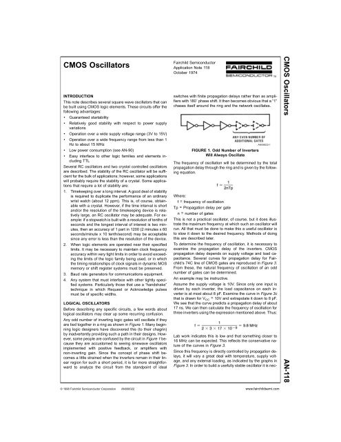
Any odd number of inverting logic gates will oscillate if they<br />
are tied together in a ring as shown in Figure 1. Many beginning<br />
logic designers have discovered this (to their chagrin)<br />
by inadvertently providing such a path in their designs. However,<br />
some people are confused by the circuit in Figure 1 because<br />
they are accustomed to seeing sinewave oscillators<br />
implemented with positive feedback, or amplifiers with<br />
non-inverting gain. Since the concept of phase shift becomes<br />
a little strained when the inverters remain in their linear<br />
region for such a short period, it is far more straightforward<br />
to analyze the circuit from the standpoint of ideal<br />
<strong>Fairchild</strong> <strong>Semiconductor</strong><br />
<strong>Application</strong> <strong>Note</strong> <strong>118</strong><br />
October 1974<br />
switches with finite propagation delays rather than as amplifiers<br />
with 180˚ phase shift. It then becomes obvious that a “1”<br />
chases itself around the ring and the network oscillates.<br />
FIGURE 1. Odd Number of Inverters<br />
Will Always Oscillate<br />
AN006022-1<br />
The frequency of oscillation will be determined by the total<br />
propagation delay through the ring and is given by the following<br />
equation.<br />
Where:<br />
f = frequency of oscillation<br />
Tp = Propagation delay per gate<br />
n = number of gates<br />
This is not a practical oscillator, of course, but it does illustrate<br />
the maximum frequency at which such an oscillator will<br />
run. All that must be done to make this a useful oscillator is<br />
to slow it down to the desired frequency. Methods of doing<br />
this are described later.<br />
To determine the frequency of oscillation, it is necessary to<br />
examine the propagation delay of the inverters. <strong>CMOS</strong><br />
propagation delay depends on supply voltage and load capacitance.<br />
Several curves for propagation delay for <strong>Fairchild</strong>’s<br />
74C line of <strong>CMOS</strong> gates are reproduced in Figure 3.<br />
From these, the natural frequency of oscillation of an odd<br />
number of gates can be determined.<br />
An example may be instructive.<br />
Assume the supply voltage is 10V. Since only one input is<br />
driven by each inverter, the load capacitance on each inverter<br />
is at most about 8 pF. Examine the curve in Figure 3c<br />
that is drawn for VCC = 10V and extrapolate it down to 8 pF.<br />
We see that the curve predicts a propagation delay of about<br />
17 ns. We can then calculate the frequency of oscillation for<br />
three inverters using the expression mentioned above. Thus:<br />
Lab work indicates this is low and that something closer to<br />
16 MHz can be expected. This reflects the conservative nature<br />
of the curves in Figure 3.<br />
Since this frequency is directly controlled by propagation delays,<br />
it will vary a great deal with temperature, supply voltage,<br />
and any external loading, as indicated by the graphs in<br />
Figure 3. In order to build a usefully stable oscillator it is nec-<br />
© 1998 <strong>Fairchild</strong> <strong>Semiconductor</strong> Corporation AN006022 www.fairchildsemi.com<br />
<strong>CMOS</strong> <strong>Oscillators</strong> AN-<strong>118</strong>
essary to add passive elements that determine oscillation<br />
frequency and minimize the effect of <strong>CMOS</strong> characteristics.<br />
STABLE RC OSCILLATOR<br />
Figure 2 illustrates a useful oscillator made with three inverters.<br />
Actually, any inverting <strong>CMOS</strong> gate or combination of<br />
gates could be used. This means left over portions of gate<br />
packages can be often used. The duty cycle will be close to<br />
50% and will oscillate at a frequency that is given by the following<br />
expression.<br />
FIGURE 2. Three Gate Oscillator<br />
Propagation Delay vs<br />
Ambient Temperature<br />
MM54C00/MM74C00,<br />
MM54C02/MM74C02,<br />
MM54C04/MM74C04<br />
(a)<br />
AN006022-3<br />
AN006022-2<br />
Propagation Delay vs<br />
Ambient Temperature<br />
MM54C00/MM74C00,<br />
MM54C02/MM74C02,<br />
MM54C04/MM74C04<br />
(b)<br />
AN006022-4<br />
FIGURE 3. Propagation Delay for 74C Gates<br />
Propagation Delay Time vs<br />
Load Capacitance<br />
MM54C00/MM74C00,<br />
MM54C02/MM74C02,<br />
MM54C04/MM74C04<br />
AN006022-5<br />
The following three special cases may be useful. Figure 4 illustrates the approximate output waveform and the<br />
voltage V 1 at the charging node.<br />
www.fairchildsemi.com 2<br />
(c)
AN006022-6<br />
FIGURE 4. Waveforms for Oscillator in Figure 2<br />
<strong>Note</strong> that the voltage V2 will be clamped by input diodes<br />
when V1 is greater than VCC or more negative than ground.<br />
During this portion of the cycle current will flow through R2.<br />
At all other times the only current through R2 is a very minimal<br />
leakage term. <strong>Note</strong> also that as soon as V1 passes<br />
through threshold (about 50% of supply) and the input to the<br />
last inverter begins to change, V1will also change in a direction<br />
that reinforces the switching action; i.e., providing positive<br />
feedback. This further enhances the stability and predictability<br />
of the network.<br />
This oscillator is fairly insensitive to power supply variations<br />
due largely to the threshold tracking close to 50% of the supply<br />
voltage. Just how stable it is will be determined by the frequency<br />
of oscillation; the lower the frequency the more stability<br />
and vice versa. This is because propagation delay and<br />
the effect of threshold shifts comprise a smaller portion of the<br />
overall period. Stability will also be enhanced if R1 is made<br />
large enough to swamp any variations in the <strong>CMOS</strong> output<br />
resistance.<br />
TWO GATE OSCILLATOR WILL NOT NECESSARILY<br />
OSCILLATE<br />
A popular oscillator is shown in Figure 5a. The only undesirable<br />
feature of this oscillator is that it may not oscillate. This<br />
is readily demonstrated by letting the value of C go to zero.<br />
The network then degenerates into Figure 5b, which obviously<br />
will not oscillate. This illustrates that there is some<br />
value of C1 that will not force the network to oscillate. The<br />
real difference between this two gate oscillator and the three<br />
gate oscillator is that the former must be forced to oscillate<br />
by the capacitor while the three gate network will always oscillate<br />
willingly and is simply slowed down by the capacitor.<br />
The three gate network will always oscillate, regardless of<br />
the value of C1 but the two gate oscillator will not oscillate<br />
when C1 is small.<br />
(a)<br />
AN006022-7<br />
AN006022-8<br />
(b)<br />
FIGURE 5. Less Than Perfect Oscillator<br />
The only advantage the two gate oscillator has over the<br />
three gate oscillator is that it uses one less inverter. This may<br />
or may not be a real concern, depending on the gate count in<br />
each user’s specific application. However, the next section<br />
offers a real minimum parts count oscillator.<br />
A SINGLE SCHMITT TRIGGER MAKES AN<br />
OSCILLATOR<br />
Figure 6 illustrates an oscillator made from a single Schmitt<br />
trigger. Since the MM74C14 is a hex Schmitt trigger, this oscillator<br />
consumes only one sixth of a package. The remaining<br />
5 gates can be used either as ordinary inverters like the<br />
MM74C04 or their Schmitt trigger characteristics can be<br />
used to advantage in the normal manner. Assuming these<br />
five inverters can be used elsewhere in the system, Figure 6<br />
must represent the ultimate in low gate count oscillators.<br />
AN006022-9<br />
FIGURE 6. Schmitt Trigger Oscillator<br />
Voltage V 1 is depicted in Figure 7 and changes between the<br />
two thresholds of the Schmitt trigger. If these thresholds<br />
were constant percentages of V CC over the supply voltage<br />
range, the oscillator would be insensitive to variations in<br />
V CC. However, this is not the case. The thresholds of the<br />
Schmitt trigger vary enough to make the oscillator exhibit a<br />
good deal of sensitivity to V CC.<br />
3 www.fairchildsemi.com
AN-<strong>118</strong> <strong>CMOS</strong> <strong>Oscillators</strong><br />
<strong>Application</strong>s that do not require extreme stability or that have<br />
access to well regulated supplies should not be bothered by<br />
this sensitivity to V CC. Variations in threshold can be expected<br />
to run as high as four or five percent when V CC varies<br />
from 5V to 15V.<br />
LIFE SUPPORT POLICY<br />
A <strong>CMOS</strong> CRYSTAL OSCILLATOR<br />
Figure 8 illustrates a crystal oscillator that uses only one<br />
<strong>CMOS</strong> inverter as the active element. Any odd number of inverters<br />
may be used, but the total propagation delay through<br />
the ring limits the highest frequency that can be obtained.<br />
Obviously, the fewer inverters that are used, the higher the<br />
maximum possible frequency.<br />
CONCLUSIONS<br />
A large number of oscillator applications can be implemented<br />
with the extremely simple, reliable, inexpensive and<br />
versatile <strong>CMOS</strong> oscillators described in this note. These oscillators<br />
consume very little power compared to most other<br />
approaches. Each of the oscillators requires less than one<br />
full package of <strong>CMOS</strong> inverters of the MM74C04 variety.<br />
Frequently such an oscillator can be built using leftover<br />
gates of the MM74C00, MM74C02, MM74C10 variety. Stability<br />
superior to that easily attainable with TTL oscillators is<br />
readily attained, particularly at lower frequencies. These oscillators<br />
are so versatile, easy to build, and inexpensive that<br />
they should find their way into many diverse designs.<br />
FAIRCHILD’S PRODUCTS ARE NOT AUTHORIZED FOR USE AS CRITICAL COMPONENTS IN LIFE SUPPORT DE-<br />
VICES OR SYSTEMS WITHOUT THE EXPRESS WRITTEN APPROVAL OF THE PRESIDENT OF FAIRCHILD SEMI-<br />
CONDUCTOR CORPORATION. As used herein:<br />
1. Life support devices or systems are devices or systems<br />
which, (a) are intended for surgical implant into<br />
the body, or (b) support or sustain life, and (c) whose<br />
failure to perform when properly used in accordance<br />
with instructions for use provided in the labeling, can<br />
be reasonably expected to result in a significant injury<br />
to the user.<br />
<strong>Fairchild</strong> <strong>Semiconductor</strong><br />
Corporation<br />
Americas<br />
Customer Response Center<br />
Tel: 1-888-522-5372<br />
www.fairchildsemi.com<br />
FIGURE 7. Waveforms for Schmitt<br />
Trigger Oscillator in Figure 6<br />
AN006022-10<br />
<strong>Fairchild</strong> <strong>Semiconductor</strong><br />
Europe<br />
Fax: +49 (0) 1 80-530 85 86<br />
Email: europe.support@nsc.com<br />
Deutsch Tel: +49 (0) 8 141-35-0<br />
English Tel: +44 (0) 1 793-85-68-56<br />
Italy Tel: +39 (0) 2 57 5631<br />
AN006022-11<br />
FIGURE 8. Crystal Oscillator<br />
2. A critical component in any component of a life support<br />
device or system whose failure to perform can be reasonably<br />
expected to cause the failure of the life support<br />
device or system, or to affect its safety or effectiveness.<br />
<strong>Fairchild</strong> <strong>Semiconductor</strong><br />
Hong Kong Ltd.<br />
13th Floor, Straight Block,<br />
Ocean Centre, 5 Canton Rd.<br />
Tsimshatsui, Kowloon<br />
Hong Kong<br />
Tel: +852 2737-7200<br />
Fax: +852 2314-0061<br />
National <strong>Semiconductor</strong><br />
Japan Ltd.<br />
Tel: 81-3-5620-6175<br />
Fax: 81-3-5620-6179<br />
<strong>Fairchild</strong> does not assume any responsibility for use of any circuitry described, no circuit patent licenses are implied and <strong>Fairchild</strong> reserves the right at any time without notice to change said circuitry and specifications.


