USER MANUAL - Rohde & Schwarz Singapore
USER MANUAL - Rohde & Schwarz Singapore
USER MANUAL - Rohde & Schwarz Singapore

You also want an ePaper? Increase the reach of your titles
YUMPU automatically turns print PDFs into web optimized ePapers that Google loves.
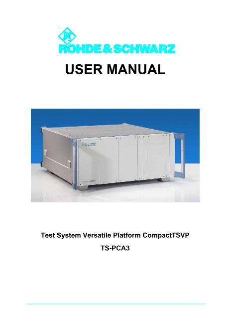
<strong>USER</strong> <strong>MANUAL</strong><br />
Test System Versatile Platform CompactTSVP<br />
TS-PCA3
User Manual<br />
for ROHDE & SCHWARZ Test System Versatile Platform CompactTSVP<br />
5th Issue / 11.05 / D 1152.3908.12<br />
All rights, also translation into foreign languages, are reserved. No part of this manual is permitted<br />
to be reproduced in any form (print, photocopy or any other method), also not for the preparation of<br />
lectures, or processed, reproduced or made available using electronic systems without written permission<br />
from ROHDE & SCHWARZ.<br />
© The passing on to third parties and the reproduction of this documentation, utilisation and communication<br />
of its contents is not permitted unless specifically approved. Infringements will incur claims<br />
for damages. All rights reserved in the case of the award of a patent or registration of a design.<br />
We draw to your attention that the names of software and hardware used in the User Manual, and<br />
the brand names of the respective companies are, in general, the subject of protection as trademarks,<br />
or under proprietary rights, or patent law.<br />
ROHDE & SCHWARZGmbH & Co. KG<br />
Corporate Headquarters<br />
Mühldorfstr. 15<br />
D-81671 München<br />
Telephone:<br />
Fax:<br />
Printed in the Federal Republic of Germany. Errors excepted, subject to technical change without notice.<br />
...49 (0)89/4129-13774<br />
...49 (0)89/4129-13777
095.1000 Bl.15<br />
Safety Instructions<br />
This unit has been designed and tested in accordance with the EC Certificate of Conformity and has left the<br />
manufacturer’s plant in a condition fully complying with safety standards.<br />
To maintain this condition and to ensure safe operation, the user must observe all instructions and warnings<br />
given in this operating manual.<br />
Observe<br />
operating<br />
instructions<br />
Safety-related symbols used on equipment and documentation from R&S:<br />
Weight<br />
indication for<br />
units >18 kg<br />
PE terminal Ground<br />
terminal<br />
1. The unit may be used only in the operating conditions<br />
and positions specified by the manufacturer.<br />
Unless otherwise agreed, the following<br />
applies to R&S products:<br />
IP degree of protection 2X, Pollution severity 2,<br />
overvoltage category 2, altitude max. 2000 m.<br />
The unit may be operated only from AC supply<br />
mains fused with max. 16 A.<br />
2. For measurements in circuits with voltages Vrms<br />
> 30 V, suitable measures should be taken to<br />
avoid any hazards.<br />
(using, for example, appropriate measuring<br />
equipment, fusing, current limiting, electrical<br />
separation, insulation).<br />
3. If the unit is to be permanently wired, the PE<br />
terminal of the unit must first be connected to<br />
the PE conductor on site before any other connections<br />
are made. Installation and cabling of<br />
the unit to be performed only by qualified technical<br />
personnel.<br />
4. For permanently installed units without built-in<br />
fuses, circuit breakers or similar protective devices,<br />
the supply circuit must be fused such as<br />
to provide suitable protection for the users and<br />
equipment.<br />
5. Prior to switching on the unit, it must be ensured<br />
that the nominal voltage set on the unit matches<br />
the nominal voltage of the AC supply network.<br />
If a different voltage is to be set, the power fuse<br />
of the unit may have to be changed accordingly.<br />
6. Units of protection class I with disconnectible<br />
AC supply cable and appliance connector may<br />
be operated only from a power socket with<br />
grounding contact and with the PE conductor<br />
con- nected.<br />
Danger!<br />
Shock hazard<br />
Warning! Hot<br />
surfaces<br />
Ground Attention!<br />
Electrostatic<br />
sensitive devices<br />
require<br />
special care<br />
7. It is not permissible to interrupt the PE conductor<br />
intentionally, neither in the incoming cable<br />
nor on the unit itself as this may cause the unit<br />
to become electrically hazardous.<br />
Any extension lines or multiple socket outlets<br />
used must be checked for compliance with<br />
relevant safety standards at regular intervals.<br />
8. If the unit has no power switch for disconnection<br />
from the AC supply, the plug of the connecting<br />
cable is regarded as the disconnecting device.<br />
In such cases it must be ensured that the power<br />
plug is easily reachable and accessible at all<br />
times (length of connecting cable approx. 2 m).<br />
Functional or electronic switches are not suitable<br />
for providing disconnection from the AC<br />
supply.<br />
If units without power switches are integrated in<br />
racks or systems, a disconnecting device must<br />
be provided at system level.<br />
9. Applicable local or national safety regulations<br />
and rules for the prevention of accidents must<br />
be observed in all work performed.<br />
Prior to performing any work on the unit or<br />
opening the unit, the latter must be disconnected<br />
from the supply network.<br />
Any adjustments, replacements of parts, maintenance<br />
or repair may be carried out only by<br />
authorized R&S technical personnel.<br />
Only original parts may be used for replacing<br />
parts relevant to safety (e.g. power switches,<br />
power transformers, fuses). A safety test must<br />
be performed after each replacement of parts<br />
relevant to safety.<br />
(visual inspection, PE conductor test, insulationresistance,<br />
leakage-current measurement, functional<br />
test).<br />
continued overleaf
10. Ensure that the connections with information<br />
technology equipment comply with IEC950 /<br />
EN60950.<br />
11. Lithium batteries must not be exposed to high<br />
temperatures or fire.<br />
Keep batteries away from children.<br />
If the battery is replaced improperly, there is<br />
danger of explosion. Only replace the battery by<br />
R&S type (see spare part list).<br />
Lithium batteries are suitable for environmentally<br />
friendly disposal or specialized recycling.<br />
Dispose of them in appropriate containers only.<br />
Do not short-circuit the battery.<br />
12. Equipment returned or sent in for repair must be<br />
packed in the original packing or in packing with<br />
electrostatic and mechanical protection.<br />
095.1000 Bl.16<br />
Safety Instructions<br />
13. Electrostatics via the connectors may damage<br />
the equipment. For the safe handling and<br />
operation of the equipment, appropriate<br />
measures against electrostatics should be<br />
implemented.<br />
14. The outside of the instrument is suitably cleaned<br />
using a soft, lint-free dustcloth. Never use<br />
solvents such as thinners, acetone or similar, as<br />
they may damage the front panel labeling or<br />
plastic parts.<br />
15. Any additional safety instructions given in this<br />
manual are also to be observed.<br />
Additional safety instructions:<br />
• Any alteration to the basic equipment is prohibited, unless carried out by persons authorized to do<br />
so according to section 9 of these safety instructions.<br />
• In case that a module is inserted which is specified for an analog bus operation < 60 VDC, then<br />
this limit is also restrictively valid for the total system.<br />
• The voltage limits for exposed voltage-carrying parts under DIN EN61010-1/6.3 must on no<br />
account be exceeded.<br />
If the use of higher voltages is required, this may be done only after consultation with R&S.<br />
• The total power which may be drawn from the secondary side depends on the format of the<br />
relevant backplane segment (typically 250VA).<br />
• When installing in racks, the ventilation of the system must be such that the specified data sheet<br />
values of 0 ... 50 °C are adhered to.
Support Center<br />
Telephone Europe: +49 180 512 42 42<br />
Telephone worldwide: +49 89 4129 13774<br />
Fax: +49 89 4129 13777<br />
e-mail: customersupport@rohde-schwarz.com<br />
If you have any technical queries about this <strong>Rohde</strong> &<br />
<strong>Schwarz</strong> equipment, our Hotline at the Support Center of<br />
<strong>Rohde</strong> & <strong>Schwarz</strong> Vertriebs-GmbH will be glad to help.<br />
Our team will discuss your queries and look for solutions to<br />
your problems.<br />
The Hotline is open Mondays to Fridays from 08.00 to 17.00<br />
hrs.<br />
For queries outside office hours, you can leave a message<br />
or send a note via fax or email. We will then get back to you<br />
as soon as possible.
5th Issue 11.05<br />
Test System Versatile Platform CompactTSVP TS-PCA3 Contents<br />
Contents<br />
1 User Information 1-1<br />
1.1 Foreword 1-1<br />
1.2 Related Documentation 1-2<br />
1.3 Purpose of the User Manual 1-3<br />
1.4 Explanation of Symbols 1-4<br />
2 Safety 2-1<br />
2.1 General 2-1<br />
2.2 Safety Instructions 2-1<br />
3 Description 3-1<br />
3.1 Usage 3-1<br />
3.1.1 General 3-1<br />
3.1.2 Explanation of Terms 3-2<br />
3.1.3 System Information 3-3<br />
3.2 Views 3-5<br />
3.3 Construction 3-7<br />
3.3.1 Case 3-7<br />
3.3.2 Slot Layout 3-8<br />
3.3.2.1 Plan View 3-8<br />
3.3.2.2 Side View 3-9<br />
3.3.3 Backplanes 3-9<br />
3.3.3.1 cPCI Backplane 3-10<br />
3.3.3.2 Analog Bus Backplane 3-15<br />
3.3.3.3 Power Backplane 3-18<br />
3.3.4 Ground Concept 3-18<br />
3.3.5 Geographical Addressing of the Slots with GA0 ... GA4 3-19<br />
3.3.6 CAN Bus 3-20<br />
3.3.7 Configurations with several Frames 3-21<br />
3.3.8 Switching the PSU 3-22<br />
3.3.9 System Controller 3-22<br />
3.3.10 Line Connection and Power Switch 3-23<br />
3.3.11 Cooling 3-23<br />
3.4 System Module TS-PSYS1 3-25<br />
3.4.1 General 3-25<br />
3.4.2 Characteristics 3-25<br />
3.4.3 Circuit Diagram of the TS-PSYS1 3-26<br />
1
2<br />
Contents Test System Versatile Platform CompactTSVP TS-PCA3<br />
3.4.4 Structure of the TS-PSYS1 3-26<br />
3.4.5 Functional Description of the TS-PSYS1 3-28<br />
3.4.5.1 Control 3-28<br />
3.4.5.2 System Functions 3-28<br />
3.4.5.3 System Clock 3-29<br />
3.4.5.4 Signal Looping 3-30<br />
3.4.5.5 Local Signal Outputs 3-30<br />
3.4.6 Driver Software 3-31<br />
3.4.7 Self-Test 3-31<br />
3.5 Function Description 3-31<br />
3.6 Permitted Module Configurations 3-32<br />
4 Commissioning 4-1<br />
4.1 Safety Instructions 4-1<br />
4.2 Setting Up 4-1<br />
4.2.1 Requirements for Repeatable Measurements 4-1<br />
4.2.2 Rack Mounting 4-1<br />
4.2.3 Desktop Setup 4-2<br />
4.3 Installation 4-3<br />
4.3.1 Safety Instructions 4-3<br />
4.3.2 Compatibility 4-3<br />
4.3.3 Module Installation 4-4<br />
4.3.4 Driver Installation 4-4<br />
4.4 Connections 4-5<br />
4.4.1 Line Inlet 4-5<br />
4.4.2 Connections at the Rear 4-5<br />
4.4.3 Connections at the Front 4-6<br />
4.5 Cabling 4-7<br />
4.5.1 Concept 4-7<br />
4.5.2 Analog Bus 4-9<br />
4.5.3 PXI Trigger Bus 4-10<br />
4.5.4 Internal Cabling of Short cPCI Modules 4-10<br />
4.5.5 External Cabling 4-11<br />
4.5.6 Opening the Case 4-12<br />
5 Operation 5-1<br />
5.1 General 5-1<br />
5.2 Powering the Unit ON and OFF 5-1<br />
5.3 Self-Test 5-3<br />
5th Issue 11.05
5th Issue 11.05<br />
Test System Versatile Platform CompactTSVP TS-PCA3 Contents<br />
6 Maintenance 6-1<br />
6.1 Important User Information 6-1<br />
6.2 Cleaning 6-1<br />
6.3 Fuse Replacement 6-2<br />
7 Plug-In Modules 7-1<br />
7.1 General 7-1<br />
7.2 Configuration Instructions 7-3<br />
7.2.1 General information 7-3<br />
7.2.2 Effects of the TS-PCA3 backplane redesign V4.0 7-3<br />
7.2.2.1 Reason 7-3<br />
7.2.2.2 Steps taken 7-4<br />
7.2.2.3 Effects 7-4<br />
8 Interface Description 8-1<br />
8.1 cPCI Backplane 8-1<br />
8.1.1 Position of Interfaces 8-1<br />
8.1.2 cPCI Connectors 8-2<br />
8.1.2.1 General 8-2<br />
8.1.2.2 Slot 1 (System) 8-3<br />
8.1.2.3 Slot 3 and 4 (cPCI peripheral) 8-4<br />
8.1.2.4 Slot 5 ... 14 (PXI peripheral / Rear I/O) 8-6<br />
8.1.2.5 Slot 15 (PXI peripheral / Rear I/O for PSYS) 8-8<br />
8.1.2.6 Slot 16 (PXI peripheral / Rear I/O) 8-10<br />
8.1.3 Connector X0 (P47) 8-11<br />
8.1.4 ATX Connectors 8-13<br />
8.1.5 Fan Connectors X90, X91, X92, X93 8-13<br />
8.1.6 Expansion Connector X80 8-14<br />
8.1.7 Jumper Field 8-14<br />
8.1.8 IPMB0 8-14<br />
8.2 Analog Bus Backplane 8-15<br />
8.2.1 Position of Interfaces 8-15<br />
8.2.2 Analog Bus Connectors X1 ... X16 8-16<br />
8.2.3 Analog Bus Connector X21 8-17<br />
8.2.4 Analog Bus Connector X22 8-18<br />
8.3 Power Backplane (Option) 8-19<br />
8.3.1 Position of Interfaces 8-19<br />
8.3.2 Power Backplane Utility Connector X13 8-19<br />
8.3.3 Power Backplane ATX Connector X12 8-20<br />
8.3.4 Power Backplane Connector X16 8-20<br />
8.3.5 Connector X1 (P47) 8-21<br />
3
4<br />
Contents Test System Versatile Platform CompactTSVP TS-PCA3<br />
8.4 Interfaces of the TS-PSYS1 8-23<br />
8.4.1 TS-PSYS1 Connector X1 8-23<br />
8.4.2 TS-PSYS1 Connector X20 8-24<br />
8.4.3 TS-PSYS1 Connector X30 8-25<br />
8.4.4 TS-PSYS1 Jumper Field X40 8-26<br />
8.4.5 TS-PSYS1 Jumper JP2 8-26<br />
8.4.6 TS-PSYS1 Jumper JP6 and JP7 8-26<br />
8.4.7 TS-PSYS1 Jumper JP8 8-27<br />
8.5 External Analog Interface 8-28<br />
8.5.1 Analog Bus Connector X2 8-28<br />
9 Technical Data 9-1<br />
9.1 Specification 9-1<br />
9.2 General Data 9-2<br />
9.3 Dimensions and Weight of the TS-PSYS1 9-3<br />
A Appendix A-1<br />
A.1 TS-PCA3 Backplane Versions A-1<br />
A.1.1 Effects of the TS-PCA3 backplane redesign A-1<br />
A.1.2 Effects of the TS-PCA3 backplane redesign V4.0 A-1<br />
A.1.2.1 Reason A-1<br />
A.1.2.2 Steps taken A-2<br />
A.1.2.3 Effects A-3<br />
A.1.3 Effects of the versions on individual modules A-4<br />
A.1.3.1 Can be used in slots 5 to 14 without any restrictions A-4<br />
A.1.3.2 Version-dependent effects A-5<br />
5th Issue 11.05
5th Issue 11.05<br />
Test System Versatile Platform CompactTSVP TS-PCA3 Figures<br />
Figures<br />
Figure 3-1 Configuration of the CompactTSVP.................................................3-3<br />
Figure 3-2 Front View ..........................................................................................3-5<br />
Figure 3-3 Rear View............................................................................................3-5<br />
Figure 3-4 Adapter Interface ...............................................................................3-6<br />
Figure 3-5 BW 2000 Case ....................................................................................3-7<br />
Figure 3-6 Plan View (Example)..........................................................................3-8<br />
Figure 3-7 Side View............................................................................................3-9<br />
Figure 3-8 Backplanes and Bus Systems..........................................................3-9<br />
Figure 3-9 CAN Bus Termination......................................................................3-11<br />
Figure 3-10 Wiring CAN bus ...............................................................................3-12<br />
Figure 3-11 Mountable Threaded Studs on the cPCI Backplane.....................3-13<br />
Figure 3-12 Connecting the current rail to AUX signals ..................................3-14<br />
Figure 3-13 Principle of the Analog Bus............................................................3-15<br />
Figure 3-14 Use of the Analog Bus in the CompactTSVP (Example)..............3-17<br />
Figure 3-15 Ground Concept ..............................................................................3-19<br />
Figure 3-16 Configuration example TS-PCA3 und TS-PWA3...........................3-21<br />
Figure 3-17 Layout of Fans in the Frame...........................................................3-24<br />
Figure 3-18 Circuit diagram of the TS-PSYS1 ...................................................3-26<br />
Figure 3-19 Connectors and Jumpers on the TS-PSYS1 .................................3-27<br />
Figure 3-20 Module Configuration TS-PCA3<br />
(Backplane Version 2.1 and 3.x).....................................................3-33<br />
Figure 3-21 Module Configuration TS-PCA3 (Backplane Version 4.0)............3-34<br />
Figure 4-1 Rear Connections..............................................................................4-5<br />
Figure 4-2 Front Connections.............................................................................4-6<br />
Figure 4-3 Inner and Internal Cabling Variants .................................................4-8<br />
Figure 4-4 Adaption of a Short PXI Module to the Adapter Interface<br />
(Example)..........................................................................................4-11<br />
Figure 4-5 CompactTSVP Rear View................................................................4-12<br />
Figure 6-1 CompactTSVP Rear View..................................................................6-2<br />
Figure 7-1 Plug-in modules in the CompactTSVP ...........................................7-1<br />
Figure 8-1 cPCI Backplane (Front View) ............................................................8-1<br />
Figure 8-2 Connectors P1 and P20 Front (Mating Side)...................................8-1<br />
5
6<br />
Figures Test System Versatile Platform CompactTSVP TS-PCA3<br />
Figure 8-3 cPCI Backplane (Rear View) .............................................................8-2<br />
Figure 8-4 Connectors P1 and P20 Rear (Mating Side) ....................................8-2<br />
Figure 8-5 Connector X0 (P47)..........................................................................8-11<br />
Figure 8-6 Analog Bus Backplane (Front View) ..............................................8-15<br />
Figure 8-7 Analog Bus Backplane (Rear View) ...............................................8-15<br />
Figure 8-8 Connectors X1 ... X16 (Mating Side)...............................................8-16<br />
Figure 8-9 Connector X21 (Mating Side) ..........................................................8-17<br />
Figure 8-10 Connector X22 (Mating Side) ..........................................................8-18<br />
Figure 8-11 Power Backplane .............................................................................8-19<br />
Figure 8-12 Connector X1 (P47) (Mating Side) ..................................................8-21<br />
Figure 8-13 TS-PSYS1 Connector X1 (Mating Side)..........................................8-23<br />
Figure 8-14 TS-PSYS1 Connector X20 (Mating Side)........................................8-24<br />
Figure 8-15 TS-PSYS1 Connector X30 (Mating Side)........................................8-25<br />
Figure 8-16 Signals at the TS-PSYS1 Jumper Field X40 ..................................8-26<br />
Figure 8-17 Signals at the TS-PSYS1 Jumper JP2............................................8-26<br />
Figure 8-18 TS-PSYS1 Jumper JP6 and JP7 .....................................................8-26<br />
Figure 8-19 Signal at the TS-PSYS1 Jumper JP8..............................................8-27<br />
Figure 8-20 Analog Bus Connector X2 (Mating Side) .......................................8-28<br />
5th Issue 11.05
5th Issue 11.05<br />
Test System Versatile Platform CompactTSVP TS-PCA3 Tables<br />
Tables<br />
Table 3-1 Software Standards ...........................................................................3-4<br />
Table 3-2 Other Characteristics ........................................................................3-4<br />
Table 3-3 Features of the BW 2000 Case .........................................................3-7<br />
Table 3-4 CAN Bus ...........................................................................................3-11<br />
Table 3-5 External Additional Signals ............................................................3-13<br />
Table 3-6 CAN Bus Termination......................................................................3-21<br />
Table 3-7 Device Addressing ..........................................................................3-22<br />
Table 3-8 Recommendations for Selecting the System Controller .............3-23<br />
Table 3-9 Characteristics of the TS-PSYS1....................................................3-25<br />
Table 3-10 Connectors on the TS-PSYS1.........................................................3-27<br />
Tabelle 5-1 PCI Configuration CompactTSVP (Example) ..................................5-2<br />
Tabelle 5-2 <strong>Rohde</strong> & <strong>Schwarz</strong> ID Numbers .........................................................5-2<br />
Table 8-1 Assignment Slot 1 .............................................................................8-3<br />
Table 8-2 Assignment Slot 3 and 4 ...................................................................8-4<br />
Table 8-3 Assignment Slot 5 ... 14 (Backplane Version 2.0 to 3.X) ................8-6<br />
Table 8-4 Assignment Slot 5 ... 14 (Backplane Version 4.X) ..........................8-7<br />
Table 8-5 Assignment Slot 15 (Backplane Version 2.0 to 3.X) .......................8-8<br />
Table 8-6 Assignment Slot 15 (Backplane Version 4.X) .................................8-9<br />
Table 8-7 Assignment Slot 16 .........................................................................8-10<br />
Table 8-8 Assignment X0 (P47) .......................................................................8-11<br />
Table 8-9 ATX Connector Assignment ...........................................................8-13<br />
Table 8-10 Assignment of X90 ... X93 ...............................................................8-13<br />
Table 8-11 Assignment of X80 ..........................................................................8-14<br />
Table 8-12 Jumper Field Assignment...............................................................8-14<br />
Table 8-13 IPMBO Assignment .........................................................................8-14<br />
Table 8-14 Assignment of X1... X16 ..................................................................8-16<br />
Table 8-15 Assignment of X21 ..........................................................................8-17<br />
Table 8-16 Assignment of X22 ..........................................................................8-18<br />
Table 8-17 Assignment of X13 ..........................................................................8-19<br />
Table 8-18 Assignment of X12 ..........................................................................8-20<br />
Table 8-19 Assignment of X16 ..........................................................................8-20<br />
7
8<br />
Tables Test System Versatile Platform CompactTSVP TS-PCA3<br />
Table 8-20 Assignment of X1 (P47)...................................................................8-21<br />
Table 8-21 TS-PSYS1 Assignment X1...............................................................8-23<br />
Table 8-22 TS-PSYS1 Assignment X20.............................................................8-24<br />
Table 8-23 TS-PSYS1 Assignment X30.............................................................8-25<br />
Table 8-24 Assignment of X2.............................................................................8-28<br />
5th Issue 11.05
5th Issue 11.05<br />
Test System Versatile Platform CompactTSVP TS-PCA3 User Information<br />
1 User Information<br />
1.1 Foreword<br />
We congratulate you on your purchase of a ROHDE & SCHWARZ Test<br />
System Versatile Platform CompactTSVP.<br />
We would emphasize that only attendance at one of our regular inhouse<br />
training seminars can ensure your successful operation of the Test<br />
System Versatile Platform in the long term.<br />
Please do not hesitate to contact us should you have any queries whilst<br />
working with the Test System Versatile Platform.<br />
We look forward to working with you<br />
GmbH & Co. KG<br />
1-1
User Information Test System Versatile Platform CompactTSVP TS-PCA3<br />
1-2<br />
1.2 Related Documentation<br />
Comprehensive documentation is supplied to enable you to use the<br />
Test System Versatile Platform CompactTSVP efficiently. The operating<br />
manual comprises the following sections:<br />
• User Information<br />
• Safety<br />
• Description<br />
• Commissioning<br />
• Operation<br />
• Maintenance<br />
• Plug-in modules<br />
• Interface description<br />
• Technical Data<br />
The Appendices contain:<br />
• Declaration of Conformity<br />
NOTE:<br />
In the event of any discrepancies between data in this manual and<br />
the technical data in the data sheet, the data sheet takes precedence.<br />
5th Issue 11.05
5th Issue 11.05<br />
Test System Versatile Platform CompactTSVP TS-PCA3 User Information<br />
1.3 Purpose of the User Manual<br />
This User Manual provides the information that is necessary for<br />
• the commissioning and<br />
• the proper and safe operation<br />
of the Test System Versatile Platform CompactTSVP.<br />
This User Manual must be carefully read by the operator/engineer who<br />
is responsible for working with the CompactTSVP before it is powered<br />
up for the first time.<br />
As well as the operating instructions and the health and safety instructions<br />
which apply at the site where the system is used, the applicable<br />
technical standards and regulations for safe and proper working must<br />
be complied with.<br />
The operating instructions must be available at or near the CompactTSVP<br />
at all times.<br />
The owner must supplement the operating instructions with national accident<br />
prevention and environmental protection regulations as appropriate.<br />
1-3
User Information Test System Versatile Platform CompactTSVP TS-PCA3<br />
1-4<br />
1.4 Explanation of Symbols<br />
The Test System Versatile Platform CompactTSVP has been manufactured<br />
in accordance with accepted engineering practice and the latest<br />
scientific and technical findings.<br />
Nevertheless there are certain risks which cannot be designed out of<br />
equipment.<br />
Additional safety instructions have been developed to provide adequate<br />
safety for the personnel working on the CompactTSVP.<br />
A satisfactory level of safety when using the CompactTSVP cannot be<br />
guaranteed unless these instructions are followed.<br />
Certain sections of text are specially highlighted. These sections have<br />
the following meaning:<br />
DANGER!<br />
Failure to follow instructions can result in personal injury!<br />
ELECTROCUTION HAZARD!<br />
Failure to follow instructions can result in personal injury!<br />
WARNING!<br />
Failure to following instructions can cause damage to the Test<br />
System Versatile Platform CompactTSVP.<br />
CAUTION!<br />
Failure to follow instructions can result in incorrect measurements.<br />
NOTE:<br />
Highlights important details to which special attention must be<br />
paid and that make work easier.<br />
5th Issue 11.05
5th Issue 11.05<br />
Test System Versatile Platform CompactTSVP TS-PCA3 Safety<br />
2 Safety<br />
2.1 General<br />
The Test System Versatile Platform must be operated in accordance<br />
with the safety regulations which apply in the owner's country.<br />
NOTE:<br />
Safety risks created by an application that is based on the Test<br />
System Versatile Platform must be eliminated by suitable additional<br />
arrangements (e.g. integration in the Emergency Stop circuit).<br />
NOTE:<br />
Failure to observe the safety regulations governing the operation<br />
of the Test System Versatile Platform shall void any liability or<br />
guarantee claims against ROHDE & SCHWARZ GmbH & Co. KG.<br />
2.2 Safety Instructions<br />
ELECTROCUTION HAZARD!<br />
The Test System Versatile Platform may only be opened by suitably<br />
trained technical personnel! The appropriate regulations<br />
governing work carried out on electrical equipment must be<br />
complied with.<br />
The CompactTSVP must be isolated from the electrical supply before<br />
work commences.<br />
WARNING!<br />
Never link out defective fuses. Always replace defective fuses with<br />
fuses of the same rating.<br />
The electrical equipment fitted to the CompactTSVP must be checked<br />
at regular intervals. Defects such as loose connections, scorched cables<br />
etc. must be rectified immediately.<br />
The enclosed safety sheet must be complied with.<br />
2-1
Safety Test System Versatile Platform CompactTSVP TS-PCA3<br />
2-2<br />
5th Issue 11.05
5th Issue 11.05<br />
Test System Versatile Platform CompactTSVP TS-PCA3 Description<br />
3 Description<br />
3.1 Usage<br />
3.1.1 General<br />
The Test System Versatile Platform CompactTSVP is a standardized<br />
modular platform for the program-controlled testing of modules<br />
and terminals in the factory or laboratory. With its flexible configuration<br />
and the use of worldwide standards, it can be perfectly adapted to suit<br />
the needs of the user.<br />
Larger ATE (Automatic Test Equipment) systems can be created by<br />
combining CompactTSVP (TS-PCA3) and PowerTSVP (TS-PWA3).<br />
The production test platform is intended for use with a control processor<br />
which performs the test on the test devices by means of peripheral<br />
modules. This control processor is known as the system controller<br />
and should preferably be in the CompactTSVP. However a standard<br />
PC can also be used running across a suitable interface with the controller.<br />
The system controller executes user-created sequences that<br />
define the test procedures and specification limits.<br />
The modules plugged into the CompactTSVP can be used for the creation<br />
of test and control signals and for the measuring related evaluation<br />
of the response from the UUT. For this purpose they are able to<br />
pass signals between each other and select signals under program<br />
control and pass them to external measuring systems.<br />
The peripheral modules can be quickly and flexibly adapted to the test<br />
devices by preceding the CompactTSVP with an adapter frame which<br />
connects the signals securely and with a low rate of wear.<br />
If the production test requires switching functions with a large number<br />
of channels or the switching of high currents, then the CompactTSVP<br />
can be supplemented with up to four PowerTSVP's. The Power-TSVP<br />
is controlled via the CAN-Bus of the CompactTSVP by the system controller.<br />
A second CompactTSVP can also be triggered.<br />
3-1
Description Test System Versatile Platform CompactTSVP TS-PCA3<br />
3-2<br />
3.1.2 Explanation of Terms<br />
The following terms and standards are used in this manual:<br />
CompactPCI (abbreviated to “cPCI” in this document) is an open standard<br />
of the PICMG (PCI Industrial Manufacturers Group) that adapts the<br />
PCI standard for industrial applications. It uses high-grade connection<br />
techniques and mechanical components, and applies the same electrical<br />
specifications as the PCI standard. This makes it possible to use inexpensive<br />
components and existing PCI developments even under industrial<br />
conditions. Other features include a high integration density, the option<br />
of a 19" installation and shielding for the plug-in modules. Its definition<br />
as an open standard means that a large, worldwide variety of cards<br />
is available.<br />
PXI (PCI eXtensions for Instrumentation) is a standard defined by National<br />
Instruments which expands the CompactPCI, using its mechanical<br />
specifications and the connection with the system controller. The<br />
PXI standard is fully compatible and also defines a number of additional<br />
signals which are useful for measuring applications, such as the PXI<br />
Triggerbus.<br />
PCI-PCI bridges are used to connect a number of cPCI or PXI segments,<br />
thereby increasing the number of peripheral slots in cPCI or PXI<br />
systems.<br />
CAN (Controller Area Network) is a serial bus system whose high system<br />
and configuration flexibility is achieved by a content-oriented addressing<br />
scheme, i.e. it defines so-called “message identifiers“ and not<br />
device addresses. Systems can be added to an existing network without<br />
the need for hardware or software modifications. The CAN protocol<br />
is defined in ISO 11898.<br />
Rear I/O is the name given to a design that allows input and output lines<br />
of the cPCI connectors P1 and P2 to be accessed from the rear of a<br />
backplane. Pluggable Rear I/O modules can be used for this purpose<br />
in the CompactTSVP and the PowerTSVP.<br />
5th Issue 11.05
5th Issue 11.05<br />
Test System Versatile Platform CompactTSVP TS-PCA3 Description<br />
Bus Slot<br />
CompactPCI<br />
PXI<br />
CAN<br />
Analog Bus<br />
Rear I/O<br />
DC/DC, Rear I/O<br />
Power Supplies<br />
3.1.3 System Information<br />
Figure 3-1 Configuration of the CompactTSVP<br />
The CompactTSVP has a modular structure that allows a range of system<br />
configurations tailored to the specific needs of the user.<br />
Up to 13 cPCI/PXI modules can be fitted in addition to the system controller<br />
(slot 1). A further slot (slot 16) is provided for special R&S plugin<br />
modules (without J1 connector). Slots A3, A4 are fitted with a PSU<br />
as standard. An optional PSU can be fitted to slots A1, A2. Slots 1 to<br />
16 provide access to the analog bus. The CAN bus is available at slots<br />
5 to 16 (starting with backplane version V4.x in slots 3 and 4 as well).<br />
There is space for rear I/O modules in the rear section of the CompactTSVP<br />
.<br />
The configuration of the CompactTSVP is shown in Figure 3-1.<br />
CPU<br />
A1 A2 A3 A4 1 2 3 4 5 6 7 8 9 10 11 12 13 14 15 16<br />
X X<br />
X with Backplane Version V4.x<br />
Starting with backplane version V4.x, some changes have been made<br />
to details to avoid incompatibilities with some third-party modules. The<br />
effects on the configurability of modules are described in Section 7.2.<br />
3-3
Description Test System Versatile Platform CompactTSVP TS-PCA3<br />
3-4<br />
The use of standard industrial PC's as system controllers makes it possible<br />
to run a wide range of software packages from the PC sector.<br />
Software Standards<br />
Operating system: Windows NT () / Windows 2000 () / Windows XP ()<br />
Test software: LabWindows/CVI () , Visual C++(r), TestStand ()<br />
Card drivers : Drivers based on VISA/IVI<br />
Table 3-1 Software Standards<br />
Table 3-2 summarizes some further characteristics of the CompactTSVP<br />
that are important for a Test System Versatile Platform.<br />
Other Characteristics<br />
Powerful cPCI PSU for 250 W (expandable to 500 W)<br />
Slot CPU's of different power classes can be used<br />
The internal analog bus facilitates the distribution of measurement/stimuli<br />
signals between the cPCI plug-in modules without additional<br />
cabling.<br />
Optional: Front mounted adapter interface on the CompactTSVP<br />
that uses spring contacts to facilitate rapid and high-pole contacting<br />
with the test devices (see Figure 3-4 ).<br />
System serviceability is monitored by a built-in self-test capability<br />
and system monitor (operating voltages, temperature)<br />
Table 3-2 Other Characteristics<br />
5th Issue 11.05
5th Issue 11.05<br />
Test System Versatile Platform CompactTSVP TS-PCA3 Description<br />
Test System Versatile Platform<br />
CompactTSVP<br />
Figure 3-2 Front View<br />
X4<br />
Figure 3-3 Rear View<br />
3.2 Views<br />
Figure 3-2 and Figure 3-3 show the CompactTSVP with slots covered.<br />
X3<br />
X2<br />
ANALOG<br />
BUS<br />
X1<br />
1<br />
0<br />
3-5
Description Test System Versatile Platform CompactTSVP TS-PCA3<br />
3-6<br />
The CompactTSVP can be operated with an adapter interface (optional)<br />
which is flange-mounted to the front panel (see Figure 3-4)<br />
Figure 3-4 Adapter Interface<br />
5th Issue 11.05
5th Issue 11.05<br />
Test System Versatile Platform CompactTSVP TS-PCA3 Description<br />
3.3 Construction<br />
3.3.1 Case<br />
The CompactTSVP uses the standard ROHDE & SCHWARZ case of<br />
the “Design 2000” (see Figure 3-5). The characteristics of the case are<br />
summarized in the Table 3-3.<br />
Figure 3-5 BW 2000 Case<br />
HF-immune case to <strong>Rohde</strong> & <strong>Schwarz</strong> “Design 2000”<br />
Dimensions: 19", height 4U, 430 mm deep<br />
Use as desktop unit or rack-mounted case<br />
Mounted in 19" rack using the telescopic slide set or on support rails<br />
Side case handles that remain on the unit when mounted in the rack.<br />
Four rugged detachable rubber feet provide rear protection.<br />
Unused slots can be covered by front sub-panels that maintain the integrity<br />
of the HF-immunity. Contact springs are mounted between the<br />
individual front sub-panels for this purpose.<br />
The case is suitable for 3U high plug-in boards.<br />
The remaining space in the case can be used for adaption to the<br />
standard UUT connector or for concealed (cross) cabling.<br />
Table 3-3 Features of the BW 2000 Case<br />
3-7
Description Test System Versatile Platform CompactTSVP TS-PCA3<br />
3-8<br />
3.3.2 Slot Layout<br />
3.3.2.1 Plan View<br />
Figure 3-6 Plan View (Example)<br />
5th Issue 11.05
5th Issue 11.05<br />
Test System Versatile Platform CompactTSVP TS-PCA3 Description<br />
3.3.2.2 Side View<br />
Figure 3-7 Side View<br />
3.3.3 Backplanes<br />
The CompactTSVP contains the following backplanes:<br />
• cPCI backplane with PICMG Power Interface and Rear I/O support<br />
• Analog bus backplane<br />
• Power backplane with PICMG Power Interface (optional)<br />
Figure 3-8 shows the backplanes with the bus systems. The assignment<br />
of the connectors is detailed in Section 8.<br />
P20<br />
Analog Bus<br />
Figure 3-8 Backplanes and Bus Systems<br />
P1<br />
Fan<br />
cPCI Backplane<br />
Rear I/O<br />
R&S Analog bus PXI Sync-Bus Auxiliary<br />
I2C CAN<br />
Slot 1 2 3 4 5 6 7 8 9 10 11 12 13 14 15 16<br />
3-9
Description Test System Versatile Platform CompactTSVP TS-PCA3<br />
3-10<br />
3.3.3.1 cPCI Backplane<br />
The cPCI backplane is implemented as follows:<br />
• 3U<br />
• 72HP<br />
• 32 bit<br />
• 33 MHz<br />
• V I/O = 5 V<br />
The backplane fulfils the Hot-Swap capability according to Standard<br />
PICMG 2.1 Rev. 2.0 for the exchange of measuring and control cards<br />
during operation. The 32 bit area conforms to PICMG 2.0 Rev. 3.0. It<br />
should be noted that ROHDE & SCHWARZ TSVP modules (TS-XXX)<br />
are not capable of hot swapping.<br />
Connector X0 (P47) serves as a power interface for a cPCI standard<br />
PSU. An additional PSU can be plugged onto an optional power backplane,<br />
in which case the connection with the cPCI backplane is made<br />
with an ATX power supply cable.<br />
Slots 1 to 8 are the first bus segment. Slots 9 to 15 form the second bus<br />
segment that is connected to the first with a PCI-PCI bridge.<br />
Slot 15 with its rear exit for the P1 signals is designed to control the system<br />
module.<br />
The Rear I/O conforms to IEEE 1101.11-1998. The P20 connectors at<br />
slots 3 and 4 are manufactured to cPCI standard, 32 bit with Rear I/O.<br />
Voltages up to 125 VDC can be applied at pins provided in the Rear I/O<br />
area.<br />
Signals PXI_TRIG0 ... 7 and PXI_CLK10 according to standard PXI<br />
R2.0 are available at the P20 connections in slots 5 to 16.<br />
Local bus<br />
The PXI local bus is not implemented. If necessary, wiring can be created<br />
between adjacent slots by plugging in a customer-specific connection<br />
board (plugged into the backplane).<br />
5th Issue 11.05
5th Issue 11.05<br />
Test System Versatile Platform CompactTSVP TS-PCA3 Description<br />
CAN-Bus<br />
The CAN bus *[1] is integrated as a further system bus in addition to<br />
the IPMB0 (slots 3 to 14) according to System Management Specification<br />
PICMG 2.9 R1.0, and is available at slots 5 to 16 (starting with<br />
backplane version V4.x in slots 3 and 4 as well). Signals CAN_L and<br />
CAN_H can be terminated at the bus end with a jumper and 120 Ohm<br />
resistor ( Figure 3-9 ). Alternatively the bus can be extended externally<br />
with an X80 expansion connector.<br />
*[1] to standard CAN 2.0b (1Mbit)<br />
Figure 3-9 CAN Bus Termination<br />
Number<br />
Lines<br />
U max<br />
(VDC)<br />
In the old design V1.0 - V3.0, the CAN bus is bussed directly, guided<br />
via PXI local bus lines LBL10 and LBL11. In the most unfavourable<br />
case, this resulted in conflicts with other PXI modules that were using<br />
the lines in a different way.<br />
In the new design V4.0, the CAN bus is switched by PSYS1 to Slot15<br />
and is directed to the other slots 3-14. The two signals are only<br />
switched by PhotoMOS relays on the backplane to the pins of a slot if<br />
a CAN module is detected in that slot. In that case the switch behaves<br />
like an isolating relay and does not affect the signals of the LBxx. It is<br />
able to isolate voltages up to ±60 V DC.<br />
PCI slots 3 + 4 now have this switch in the backplane and are thus<br />
CAN-capable. The CAN bus is continuously connected on slots 15 + 16<br />
without switching.<br />
Pin<br />
2 5 CAN_H: P20/C1<br />
CAN_L: P20/D1<br />
Table 3-4 CAN Bus<br />
3-11
Description Test System Versatile Platform CompactTSVP TS-PCA3<br />
3-12<br />
A 330-Ohm pull-up resistor between P2/D18 and +5 V on each module<br />
is responsible for detecting a CAN module and activating the CAN bus.<br />
Normal cPCI or PXI modules according to specification apply this pin to<br />
GND or leave it open. This ensures the CAN bus is never in conflict with<br />
analogue voltages of the local bus.<br />
Measurement Module<br />
+5V<br />
P2/D18<br />
P2/D18<br />
330R<br />
100R<br />
Figure 3-10 Wiring CAN bus<br />
1/2*AQS225<br />
Backplane<br />
CAN_H<br />
CAN_L<br />
P2/C1<br />
P2/D1<br />
5th Issue 11.05
5th Issue 11.05<br />
Test System Versatile Platform CompactTSVP TS-PCA3 Description<br />
External additional signals (AUX)<br />
Two additional external signals (for example power supply voltages)<br />
can be fed into a module via J20 on slots 5 through 16. The signals can<br />
be fed in in the area of the CPCI power pack by the CPCI power supply,<br />
an internal AC/DC module or another external signal sources. This can<br />
be used to provide a primary voltage to generate local supply voltages<br />
(DC/DC converter), etc.<br />
Number<br />
Lines<br />
U max<br />
(VDC)<br />
I /Slot(A<br />
max<br />
DC)<br />
+5-V and +12-V lines from the P47 connector are routed on the screw<br />
bolts above slot 4. This makes it easy to connect AUX1 with +5 V and<br />
AUX2 with +12 V via current rail or cable (see Figure 3-11 ).<br />
The AUX pins assigned to slots 5 - 16 make it possible to direct two<br />
voltages from the current rail on the upper backplane if a screw there<br />
connects the backplane signals with the current rail. Currently in backplanes<br />
V1.1 through V3.0 two pins are hard connected to carry a higher<br />
current.<br />
Pin<br />
2 60 2 Input for ext. signals:<br />
J20: AUX1 B20, E19<br />
J20: AUX2 A20, D19<br />
Table 3-5 External Additional Signals<br />
+5V<br />
+12V<br />
5 4 3 2 Slot 1<br />
Figure 3-11 Mountable Threaded Studs on the cPCI Backplane<br />
X0<br />
3-13
Description Test System Versatile Platform CompactTSVP TS-PCA3<br />
3-14<br />
This is changed in backplane V4.0 so the two pins are not connected<br />
in normal state. One pin (for example AUX1L) on the solder side is directed<br />
to the current rail and one pin (AUX1R) on the module side is<br />
directed to the current rail as well. The connection is not made until a<br />
screw with a nut is screwed in and connects the current rail and the two<br />
copper rings in the layout. It may be preferably to insert a toothed washer<br />
to ensure better contact.<br />
Functionally this is no different than the previous version. The PXI<br />
specification is observed except for the lack of a local bus daisy chain.<br />
Full current must not be drawn unless the two pins are connected in<br />
parallel.<br />
Figure 3-12 Connecting the current rail to AUX signals<br />
5th Issue 11.05
5th Issue 11.05<br />
Test System Versatile Platform CompactTSVP TS-PCA3 Description<br />
Analogbus<br />
3.3.3.2 Analog Bus Backplane<br />
To simplify cabling, the CompactTSVP contains an analog bus with 8<br />
signals. The analog bus backplane is located in the front above the<br />
cPCI backplane. A special layout meets the need for high crosstalk<br />
damping and low capacitance of the signal lines to GND.<br />
The C module (2 mm connector system) is used as the connectors<br />
(X1...X16). Plug-in modules with no analog bus connector access the<br />
analog bus via a 26-pin connector (X22) and R&S switch modules. Signals<br />
IL1_x and IL2_x (Instrument Line) are passed from slots 5 to 16 to<br />
connector X22.<br />
The analog bus signals pass from connector X21 to connector X2 at the<br />
back of the CompactTSVP (see Section 4/4/2).<br />
The electrical characteristics of the analog lines are:<br />
• Voltage 125 VDC max.<br />
• Current 1 A max.<br />
3.3.3.2.1 Concept of the Analog Bus<br />
Instrument-Pins<br />
Figure 3-13 Principle of the Analog Bus<br />
I/O-Channels<br />
UUT<br />
UUT-Pins<br />
The analog bus in the CompactTSVP connects I/O channels of different<br />
plug-in modules to each other. These I/O channels may be connections<br />
of instruments (measuring and stimuli devices) and connections<br />
3-15
Description Test System Versatile Platform CompactTSVP TS-PCA3<br />
3-16<br />
of the test device. Up to 8 signals can be connected simultaneously<br />
(see Figure 3-13 ).<br />
The analog bus can be used flexibly with the ROHDE & SCHWARZspecific<br />
plug-in modules. 8 equivalent lines are basically available<br />
(ABa1, ABa2, ABb1, ABb2, ABc1, ABc2, ABd1, ABd2). External instruments<br />
are usually connected to the CompactTSVP with a rear I/O connection.<br />
The signals for the test device are made available at the frontend<br />
connector of the various plug-in modules on the CompactTSVP.<br />
The analog bus can be used in different ways:<br />
• as 1 bus with 8 lines<br />
• in 2 part-buses with 4 lines each<br />
The split of the analog bus into part-buses depends on the plug-in modules<br />
which are used.<br />
The analog bus concept of the CompactTSVP fully meets the requirements<br />
that are frequently made in metrology:<br />
• A small number of buses for a high number of I/O channels (e.g.<br />
In-Circuit-Test with 3 to 6 buses.)<br />
• As many signals as possible simultaneously for a moderate<br />
number of I/O channels (e.g. function test with 8 buses of 50 to 100<br />
I/O channels).<br />
• Parallel test with split analog bus.<br />
Line paths or higher-frequency signals are usually connected locally by<br />
special switching modules and not via the analog bus.<br />
5th Issue 11.05
5th Issue 11.05<br />
Test System Versatile Platform CompactTSVP TS-PCA3 Description<br />
Modular Measurement Module<br />
TS-PSAM<br />
Modular Switching Modules<br />
UUT<br />
3.3.3.2.2 Typical Use of the Analog Bus<br />
The use of the analog bus and individual bus lines is illustrated with<br />
available R&S modules and standard modules (see Figure 3-14 ).<br />
Internal Access to Analog<br />
Bus or Switching (X22)<br />
PXI-Module<br />
Analog Bus<br />
Figure 3-14 Use of the Analog Bus in the CompactTSVP (Example)<br />
Matrix<br />
Matrix<br />
cPCI Backplane<br />
Analog Bus Connector<br />
(rear) for Monitoring<br />
Instrument Lines<br />
ATE Module TS-PMB<br />
Rear-I/O-Access<br />
to Analog Bus for<br />
External Instruments<br />
External<br />
Instrument<br />
3-17
Description Test System Versatile Platform CompactTSVP TS-PCA3<br />
3-18<br />
3.3.3.3 Power Backplane<br />
The use of a second cPCI PSU in slots A1, A2 requires the optional<br />
Power Backplane (conforms to standard PICMG 2.0). From the Power<br />
Backplane, a cable with three connectors leads to a 24-pin ATX connector<br />
on the cPCI backplane. The three connectors are as follows<br />
(see also Section 8, Interface Description):<br />
• X12, 20-pin<br />
• X13, 10-pin<br />
• X16, 4-pin<br />
The second PSU can be used to boost the power of the standard PSU<br />
when connected in parallel. Alternatively it can be used to supply the<br />
device on test.<br />
3.3.4 Ground Concept<br />
An electrically conductive CHA-GND (chassis GND) pad in the mounting<br />
area on the cPCI backplane provides an impedance grounding to<br />
the chassis. Screw connections and a busbar on the cPCI backplane<br />
are used to make a low-resistance connection for GND and CHA-GND,<br />
while a star connection between GND and CHA-GND using a busbar<br />
prevents unwanted ground loops.<br />
A capacitor creates the HF connection between GND and CHA-GND at<br />
each slot. A 1 MOhm resistor discharges the capacitors and dissipates<br />
static.<br />
A 3-pin connector provides the 230 VAC supply for the cPCI PSU on<br />
the cPCI backplane (at X0).<br />
The optional power backplane is supplied with AC voltage parallel to<br />
the cPCI backplane.<br />
The PE conductor must be bonded to the case with a grounding cable.<br />
The GND signal of the analog bus backplane is connected by a cable<br />
and screw terminal to the GND on the cPCI backplane. This prevents<br />
the large induction loops that would occur if a return via chassis were<br />
to be used.<br />
5th Issue 11.05
5th Issue 11.05<br />
Test System Versatile Platform CompactTSVP TS-PCA3 Description<br />
Power<br />
Backplane<br />
AC Input PE N L<br />
Power Filter<br />
PE N L<br />
CompactTSVP<br />
Figure 3-15 Ground Concept<br />
The ground screen of the analog bus between two basic CompactTSVP<br />
units is connected to CHA-GND (chassis). An alternative<br />
screen can also be made with GND, but the first option offers better<br />
screening performance.<br />
In the second CompactTSVP CHA-GND must not be connected to<br />
GND to prevent ground loops. The connections are indicated in<br />
Figure 3-15.<br />
GND sense of +5 V and +3.3 V (of the second PSU as well) are connected<br />
to GND at the grounding star point.<br />
Analog bus<br />
Screen<br />
CHA-GND GND CHA-GND GND<br />
cPCI-Backplane<br />
Analog bus<br />
GND GND<br />
Rack connection<br />
cPCI-Backplane<br />
CompactTSVP<br />
3.3.5 Geographical Addressing of the Slots with GA0 ... GA4<br />
The physical slot addresses are coded by the signals GA0 ... GA4 of<br />
the P20 connector (see the cPCI specification). These signals are either<br />
connected to GND or remain open. In order to distinguish two interconnected<br />
CompactTSVP , GA4 is defined by Jumper 1. The jumper<br />
is closed for the first Compact-TSVP (see jumper field in Section 8).<br />
3-19
Description Test System Versatile Platform CompactTSVP TS-PCA3<br />
3-20<br />
The coding for slot recognition is carried out with GA0 ... GA3 as follows:<br />
1<br />
2<br />
3<br />
4<br />
5<br />
6<br />
7<br />
8<br />
9<br />
10<br />
11<br />
12<br />
13<br />
14<br />
15<br />
16<br />
Slot Code<br />
Note:<br />
0: Pin connected to GND via resistor<br />
1: Pin open<br />
3.3.6 CAN Bus<br />
For controlling of the switch modules TS-PMB and TS-PSM1 as well as<br />
the control modules TS-PSYS1 and TS-PSYS2, the CAN bus is used<br />
in TS-PCA3 and TS-PWA3. The CAN bus numbering results from the<br />
following scheme:<br />
CANu::v::w::x<br />
0001<br />
-<br />
0010<br />
0011<br />
0100<br />
0101<br />
0110<br />
0111<br />
1000<br />
1001<br />
1010<br />
1011<br />
1100<br />
1101<br />
1110<br />
1111<br />
u = Board Number<br />
v = Controller Number<br />
w = Device Number<br />
x = Slot Number<br />
Board Number and Controller Number are always 0. The Device<br />
Number of the frame is determined by the settings of the jumpers on<br />
the backplane (see Section 3.3.7). For Rear-I/O modules like TS-<br />
PSYS1 and TS-PSYS2, a 4 has to be added to the Device Number.<br />
5th Issue 11.05
5th Issue 11.05<br />
Test System Versatile Platform CompactTSVP TS-PCA3 Description<br />
Example: CAN0::0::5::15<br />
Board Number: 0<br />
Controller Number: 0<br />
Device Number: 5 (Device 1, Rear-I/O)<br />
Slot Number: 15<br />
The following table shows the jumper configuration for the bus terminations<br />
CAN1 (System) und CAN2 (User).<br />
Modul CAN-Bus offen terminiert<br />
TS-PCA3 CAN1 (System) Jumper J3 and<br />
Jumper J4 open<br />
TS-PWA3 CAN1 (System) Jumper J4 and<br />
Jumper J5 open<br />
3.3.7 Configurations with several Frames<br />
Jumper J3 and Jumper J4<br />
geschlossen<br />
Jumper J4 and Jumper J5<br />
closed<br />
TS-PSYS1, TS-PSYS2 CAN1 (System) Jumper JP6 open Jumper JP6 closed<br />
TS-PSYS1, TS-PSYS2 CAN2 (User) Jumper JP7 open Jumper JP7 closed<br />
Table 3-6 CAN Bus Termination<br />
J3, J4 closed<br />
J4, J5 closed<br />
In the following figure, the terminating resistors are depicted in yellow.<br />
CompactTSVP TS-PCA3<br />
PowerTSVP TS-PWA3<br />
Figure 3-16 Configuration example TS-PCA3 und TS-PWA3<br />
TS-PSYS1<br />
TS-PSYS2<br />
JP6 open<br />
JP7 closed<br />
JP6 open<br />
3-21
Description Test System Versatile Platform CompactTSVP TS-PCA3<br />
3-22<br />
CAN1 (System) is being connected between the two frames via cable<br />
TS-PK02 (option). The termination is carried out on both backplanes.<br />
The jumpers on the system modules TS-PSYS1 and TS-PSYS2 have<br />
to be left open.<br />
According to Section 3.3.5, the jumpers for device addressing must be<br />
set as follows:<br />
TS-PCA3: J1 set → Device 1<br />
TS-PWA3: J1 set, J2 not set → Device 2<br />
J1 (GA4) J2 (GA5) Device<br />
set set 1<br />
set not set 2<br />
not set set 3<br />
not set not set 4<br />
Table 3-7 Device Addressing<br />
3.3.8 Switching the PSU<br />
Signal PS-ON is used to switch the PSU outputs on and off. This is<br />
done by removing Jumper 2 (see jumper field in Section 8) and replacing<br />
it by an external switch. Signal PS-ON is available at expansion<br />
connector X80.<br />
3.3.9 System Controller<br />
Operating the CompactTSVP requires the use of a system controller.<br />
This is fitted to slot 1. The CompactTSVP allows the use of standard<br />
cPCI or PXI system controllers (e.g. PEP CP304).<br />
5th Issue 11.05
5th Issue 11.05<br />
Test System Versatile Platform CompactTSVP TS-PCA3 Description<br />
Alternatively an external PC can be used, and suitable PCI-to-cPCI interfaces<br />
are available on the market. Table 3-8 lists basic data which a<br />
system controller should meet for the practical operation of the Test<br />
System Versatile Platform .<br />
cPCI Interface Specification<br />
Processor 1 GHz Pentium III or faster, passive cooling<br />
L2 Cache 256 Kbytes<br />
RAM Min. 256 MB SDRAM<br />
Front Side Bus Min. 100 MHz<br />
Hard drive 2.5", Min. 20 GB<br />
VGA Onboard<br />
Ethernet 10 Base-T / 100 Base-TX, RJ45 Connector<br />
Serial Port COM1, Front Panel<br />
Keyboard Connector PS/2, Front Panel, USB<br />
Mouse Connector PS/2, Front Panel, USB<br />
USB USB Interface<br />
EIDE HDD<br />
Temperature 0 ... 60 °C<br />
Humidity 0 ... 95%<br />
Table 3-8 Recommendations for Selecting the System Controller<br />
3.3.10 Line Connection and Power Switch<br />
The line inlet and power switch are at the back of the CompactTSVP<br />
(see Figure 3-3 ).<br />
3.3.11 Cooling<br />
The CompactTSVP features a powerful cooling concept.<br />
The slots at the front (optional in the Rear I/O area) are cooled by a vertical<br />
flow of air. The four fans are located above the slots (see<br />
Figure 3-17 ) and are connected by inline contact connectors to the<br />
backplane. The fan speed is regulated by the internal temperature.<br />
Fans for the Rear I/O area can be retrofitted if required. The supply for<br />
these fans can be taken off expansion connector X80.<br />
3-23
Description Test System Versatile Platform CompactTSVP TS-PCA3<br />
3-24<br />
WARNING!<br />
Adequate space for air inlet and outlet should be allowed when the<br />
case is rack mounted, with at least half a height unit (22 mm) being<br />
left above and below the chassis!<br />
For desktop mounting, ensure that the case is not covered over!<br />
Figure 3-17 Layout of Fans in the Frame<br />
5th Issue 11.05
5th Issue 11.05<br />
Test System Versatile Platform CompactTSVP TS-PCA3 Description<br />
3.4 System Module TS-PSYS1<br />
3.4.1 General<br />
The TS-PSYS1 is in the Rear I/O slot 15 of the CompactTSVP. It acts<br />
primarily as a cPCI-to-CAN interface and therefore as an interface for<br />
communication with R&S CAN modules in the CompactTSVP and<br />
PowerTSVP.<br />
Additional system functions such as voltage and temperature monitoring,<br />
trigger signals and optocoupler interface are used to integrate the<br />
CompactTSVP and PowerTSVP in a complete system.<br />
3.4.2 Characteristics<br />
RTM type with cPCI interface<br />
TS-PSYS1<br />
2 independent CAN interfaces (2.0 A/B, 1 Mb/s)<br />
System functions via CAN node (microcontroller)<br />
- Voltage monitor<br />
- Temperature measuring (internal)<br />
- Enable of the PXI trigger signals to the exterior<br />
- 4 optocoupler outputs<br />
- 4 optocoupler inputs<br />
- 2 switchable, short-circuit proof output voltages<br />
- System identification<br />
Manual selection of the local or external system clock, and its buffering<br />
with jumper<br />
Table 3-9 Characteristics of the TS-PSYS1<br />
3-25
Description Test System Versatile Platform CompactTSVP TS-PCA3<br />
3-26<br />
CPCI Rear I/O X20<br />
CPCI Rear I/O X1<br />
PXI_TRIG<br />
CPCI<br />
Interface<br />
PLX9050<br />
Figure 3-18 Circuit diagram of the TS-PSYS1<br />
3.4.3 Circuit Diagram of the TS-PSYS1<br />
Figure 3-18 shows the circuit diagram of the TS-PSYS1<br />
Buffer<br />
JP8 CLK10_OUT<br />
PXI_CLK10<br />
DC_SYNC<br />
Buffer<br />
Buffer<br />
J<br />
P<br />
2 CLK 10MHz<br />
Buffer<br />
CLK10_IN<br />
SYNC_OUT<br />
AUX1..6<br />
IL1..3<br />
GA0..4<br />
X<br />
4<br />
0<br />
8<br />
uC<br />
+<br />
Flash<br />
+<br />
CAN<br />
+<br />
A/D<br />
+3.3/+5V<br />
Voltage<br />
+12/-12V 2<br />
Temperature<br />
uC<br />
+<br />
CAN Controller<br />
CAN1(System)<br />
Transceiver<br />
CAN2(User)<br />
Transceiver<br />
3.4.4 Structure of the TS-PSYS1<br />
8<br />
FET Bus Switch<br />
4<br />
4<br />
Buffer<br />
Pull-Ups<br />
Protect.<br />
TRIG<br />
The TS-PSYS1 is the size of a standard cPCI-RTM (Rear Transmission<br />
Module) and is mounted in slot 15 at the rear of the TSVP chassis.<br />
+5V<br />
+12V<br />
PhotoMos<br />
Output<br />
Optocoupler<br />
Input<br />
LDO<br />
LDO<br />
6<br />
8<br />
8<br />
8<br />
AUX<br />
+4.5V<br />
+11.5V<br />
TEMP_OUT<br />
JP6<br />
Term.<br />
JP7<br />
Term.<br />
Front Connector X30<br />
5th Issue 11.05
5th Issue 11.05<br />
Test System Versatile Platform CompactTSVP TS-PCA3 Description<br />
Connectors X1 and X20 are used to make the connections to the Rear<br />
I/O side of the cPCI backplane in the CompactTSVP. Connector X30 is<br />
a 44-pin D-sub socket (High Density). Jumper field X40 as well as the<br />
Jumpers JP2, JP6, JP7and JP8 are placed on the circuit board.<br />
Figure 3-19 Connectors and Jumpers on the TS-PSYS1<br />
Symbol Use<br />
X1 cPCI Rear I/O (P1)<br />
X20 cPCI Rear I/O (P2)<br />
X30 Front Connector<br />
X40 Jumper field Rear I/O signals<br />
Table 3-10 Connectors on the TS-PSYS1<br />
3-27
Description Test System Versatile Platform CompactTSVP TS-PCA3<br />
3-28<br />
3.4.5 Functional Description of the TS-PSYS1<br />
(see also Figure 3-18 )<br />
3.4.5.1 Control<br />
The TS-PSYS1 is controlled via the cPCI interface. It provides two CAN<br />
bus channels (type 2.0 A/B to ISO 11898):<br />
• CAN1: Internal connection, for controlling the R&S modules<br />
• CAN2: General Usage<br />
The CAN lines are terminated manually with a jumper on the TS-<br />
PSYS1 (see Section 8.4)<br />
3.4.5.2 System Functions<br />
The system functions are implemented by an 8 bit microcontroller<br />
which operates at a 10 MHz system speed. It communicates with the<br />
system controller in the CompactTSVP or PC across the CAN1 port.<br />
The following functions are available:<br />
• 8 x enable of PXI trigger signals to the outside (e.g. PowerTSVP)<br />
• 4 x optocoupler outputs (for PLC or handling systems)<br />
• 4 x optocoupler inputs (for PLC or handling systems)<br />
• 2 x enable for additional supply voltages (+4.5 V / +11.5 V)<br />
• 4 x measurement of the cPCI supply voltages<br />
• 1 x measurement of the internal temperature<br />
3.4.5.2.1 PXI Trigger<br />
The input/output of trigger signals (X20) is controlled separately for<br />
each signal. On the output side the signals are terminated by pullup resistors<br />
and protected by self-healing fuses and d.c. clamp diodes. The<br />
external trigger lines are available at connector X30.<br />
3.4.5.2.2 Floating Outputs<br />
4 PhotoMos relays (with internal current limiter) are triggered by a µC<br />
port. The signals are available at connector X30.<br />
5th Issue 11.05
5th Issue 11.05<br />
Test System Versatile Platform CompactTSVP TS-PCA3 Description<br />
3.4.5.2.3 Floating Inputs<br />
A µC port reads the status of 4 optocoupler inputs (2 x 2-pin). The current<br />
at the inputs is limited so that inputs signals can be fed in unconditioned<br />
within a wide voltage range. These inputs are available at connector<br />
X30.<br />
3.4.5.2.4 Output Voltages<br />
Two voltage regulators with output-enable control generate switchable,<br />
short-circuit proof voltages of +4.5 V and +11.5 V at X30. These voltages<br />
can be used to supply external components (e.g. signal lamps).<br />
3.4.5.2.5 Measuring the cPCI Supply Voltages<br />
The supply voltages present at connector X20 (+3.3 V / +5 V / +12 V /<br />
-12 V) are measured with the A/D ports of the µC.<br />
3.4.5.2.6 Temperature Measurement<br />
An A/D port of the µC is used to measure the ambient temperature of<br />
the plug-in module. A temperature-to-voltage converter is used as the<br />
sensor. The temperature-proportional analog voltage is also output at<br />
connector X30 for monitoring purposes (TEMP_OUT).<br />
3.4.5.2.7 Geographical Addressing<br />
According to the cPCI specification, each slot is assigned its own digital<br />
slot code (GA code). This code is used internally to directly address the<br />
µC.<br />
3.4.5.3 System Clock<br />
A local quartz crystal generates the 10 MHz system pulse for the PXI<br />
system (PXI_CLK10). Alternatively a very accurate reference pulse can<br />
be fed in across X30. Jumper JP2 is used to select an internal or external<br />
clock source. The jumper functions are shown in Section 8.4.<br />
3-29
Description Test System Versatile Platform CompactTSVP TS-PCA3<br />
3-30<br />
3.4.5.4 Signal Looping<br />
A number of signal lines are looped from connector X30 to connector<br />
X20. These are used to input/output Rear I/O signals (e.g. for the R&S<br />
switching modules TS-PMB, TS-PSAM)<br />
2<br />
4<br />
Number<br />
Lines<br />
3.4.5.5 Local Signal Outputs<br />
Signal Name Current Carrying Capacity<br />
AUX1 ... 2<br />
AUX3 ... 6<br />
3 A<br />
1.5 A<br />
Special signals of the CompactTSVP can be connected to connector<br />
X20 (Rear I/O) with the help of jumper field X40. The jumper functions<br />
are described in Section 8.4.<br />
WARNING!<br />
Jumpers only permitted when system voltages are < 60 VDC<br />
Number<br />
Lines<br />
Signal Name Current Carrying<br />
Capacity<br />
3 AUX4 ... 6 1.5 A<br />
3 (6) IL1 ... 3 1.5 A<br />
2 CAN2<br />
5th Issue 11.05
5th Issue 11.05<br />
Test System Versatile Platform CompactTSVP TS-PCA3 Description<br />
3.4.6 Driver Software<br />
The TS-PSYS1 is triggered by a universal driver software. The local microcontroller<br />
is triggered by the CAN1 bus and the R&S-specific protocol.<br />
The following software modules are installed during driver installation:<br />
• RSCAN<br />
• RSPSYS<br />
3.4.7 Self-Test<br />
The TS-PSYS1 has no built-in self-test capability. The function of the<br />
internal CAN bus can be checked with the local CAN node. .<br />
3.5 Function Description<br />
The functionality of the CompactTSVP depends essentially on the installed<br />
plug-in modules and the related software. The CompactTSVP<br />
is basically suitable for all types of production tests.<br />
An adapter interface can be flange-mounted to the front of the CompactTSVP<br />
for the rapid and high-pole adaption of test devices (see<br />
Figure 3-4 )<br />
3-31
Description Test System Versatile Platform CompactTSVP TS-PCA3<br />
3-32<br />
3.6 Permitted Module Configurations<br />
Because of the different properties of plug-in modules, for example<br />
• control bus<br />
• power supply<br />
• rear-I/O module required<br />
• controller function<br />
• power pack<br />
• trigger bus required<br />
there are restrictions on the use of plug-in slots.<br />
Figure 3-20 and Figure 3-21 shows an overview of which modules can<br />
be operated in which plug-in slots.<br />
5th Issue 11.05
5th Issue 11.05<br />
Test System Versatile Platform CompactTSVP TS-PCA3 Description<br />
Test System Versatile Platform<br />
CompactTSVP<br />
CP<br />
Figure 3-20 Module Configuration TS-PCA3 (Backplane Version 2.1 and 3.x)<br />
3-33
Description Test System Versatile Platform CompactTSVP TS-PCA3<br />
3-34<br />
Test System Versatile Platform<br />
CompactTSVP<br />
CP<br />
Figure 3-21 Module Configuration TS-PCA3 (Backplane Version 4.0)<br />
5th Issue 11.05
5th Issue 11.05<br />
Test System Versatile Platform CompactTSVP TS-PCA3 Commissioning<br />
4 Commissioning<br />
4.1 Safety Instructions<br />
When commissioning the Test System Versatile Platform CompactTSVP<br />
the safety instructions in Section 2 must be followed.<br />
4.2 Setting Up<br />
4.2.1 Requirements for Repeatable Measurements<br />
The ambient conditions listed below are recommended for the installation<br />
site of a Test System Versatile Platform with CompactTSVP:<br />
• Temperature variance within 24 hours not to exceed approx. 3 °C.<br />
• Maximum temperature variance within one hour not to exceed approx.<br />
0.5 °C.<br />
• Extreme vibrations from mechanical or dynamic sources such as<br />
presses, power punches etc. must be avoided.<br />
• The TSVP should be warmed up for approx. 15 minutes before<br />
measurements commence. This time will depend on the type of<br />
measuring modules and can be longer.<br />
Compliance with these guidelines will ensure accurate and repeatable<br />
measurements.<br />
4.2.2 Rack Mounting<br />
The rack mounting kit supplied by ROHDE & SCHWARZ must be used<br />
for rack mounting the TSVP.<br />
WARNING!<br />
A minimum clearance of half a height unit should be allowed<br />
above and below the CompactTSVP !<br />
This space can be used to fit filter mats.<br />
4-1
Commissioning Test System Versatile Platform CompactTSVP TS-PCA3<br />
4-2<br />
The TSVP is installed in six steps:<br />
• Unscrew the four case feet from the base.<br />
• Screw the “19 inch brackets” contained in the rack mounting kit under<br />
the side handles, replacing the old screws with the longer<br />
screws.<br />
• Remove the four rubber tips from the unit's feet.<br />
WARNING!<br />
Do not unscrew the rear four feet as this will loosen the body of<br />
the case!<br />
• Affix the self-adhesive plastic slide rails.<br />
• Place the unit into the rack on prepared aluminum rails.<br />
• Fix the CompactTSVP by screwing the “19 inch side brackets” to<br />
the rack.<br />
NOTE:<br />
Check the position of the locknuts in the rack before sliding in<br />
the CompactTSVP.<br />
• If required, insert and attach filter mats above and below the<br />
TSVP.<br />
An optional telescopic rail set is also available. The telescopic rails<br />
are fitted to the side of the “BW 2000” case. The CompactTSVP can<br />
then be pushed into the prepared support in the rack.<br />
4.2.3 Desktop Setup<br />
When the CompactTSVP is set up on a desktop, the minimum gap under<br />
the unit is provided by the feet on the “BW 2000” case.<br />
WARNING!<br />
Do not obscure the ventilation louvers on the top of the unit!<br />
The minimum clearance of half a height unit must be ensured!<br />
5th Issue 11.05
5th Issue 11.05<br />
Test System Versatile Platform CompactTSVP TS-PCA3 Commissioning<br />
4.3 Installation<br />
4.3.1 Safety Instructions<br />
WARNING!<br />
Comply with ESD regulations (Electrostatically Sensitive Device)<br />
when fitting plug-in modules.<br />
4.3.2 Compatibility<br />
The following plug-in modules can be used in the CompactTSVP:<br />
• 32 bit standard cPCI system controller in slot 1<br />
• all 32 bit standard cPCI modules (without J2 connector).<br />
• all 32 bit standard cPCI modules (with/without Rear I/O and J2<br />
connector) in slot 3 and 4.<br />
• all 32 bit PXI modules in slots 5 to 14. At slot 15 the signal compatibility<br />
should be checked against the interface description (see<br />
Section 8), as only parts of the PXI concepts are supported (see<br />
Section 3/3/03.1).<br />
Star Trigger and the local bus of the PXI specification are not supported.<br />
WARNING!<br />
The plug-in module or the CompactTSVP can be damaged if signals<br />
are not compatible.<br />
• all new ROHDE & SCHWARZ- specific cPCI modules with cPCI<br />
interface (with J1 connector) in slots 5 to 15.<br />
• ROHDE & SCHWARZ- plug-in module only with J20 connectors in<br />
slots 5 to 16 (CAN module)<br />
4-3
Commissioning Test System Versatile Platform CompactTSVP TS-PCA3<br />
4-4<br />
4.3.3 Module Installation<br />
To install an R&S plug-in module, proceed as follows:<br />
• Run down and power off the CompactTSVP.<br />
• Select a suitable slot (see Section 4.3.2 )<br />
• Remove the appropriate front panel by slackening off the screws<br />
WARNING!<br />
Check backplane connectors for bent pins! Any bent pins must be<br />
straightened!<br />
Failure to do this may permanently damage the backplane!<br />
• Push in the plug-in module using moderate pressure<br />
• The top snap pin on the module must locate in the right-hand and<br />
the bottom pin in the left-hand hole on the TSVP chassis<br />
WARNING!<br />
Use both hands to guide the module and carefully plug it into the<br />
backplane connectors<br />
• The module is correctly located when a distinct 'stop' can be felt<br />
WARNING!<br />
When short and long modules are mounted into adjacent slots, the<br />
front panel of the short module may cause short circuits on the<br />
long module, so please ensure adequate clearance!<br />
• Tighten the top and bottom screws on the front panel of the plugin<br />
module<br />
4.3.4 Driver Installation<br />
The drivers to be installed for the plug-in modules will depend on the<br />
operating system and the module itself, and you should therefore consult<br />
the documentation supplied by the module manufacturer.<br />
5th Issue 11.05
5th Issue 11.05<br />
Test System Versatile Platform CompactTSVP TS-PCA3 Commissioning<br />
5<br />
X4<br />
Figure 4-1 Rear Connections<br />
4.4 Connections<br />
4.4.1 Line Inlet<br />
The CompactTSVP requires a supply within the range of 110 V / 60 AC<br />
Hz or 230 V / 50 Hz. Fuse protection for the line inlet must not ex-<br />
AC<br />
ceed a rating of 16 A.<br />
The PSU used in the CompactTSVP has automatic voltage selection<br />
between 100 and 240 Volt AC (see Section 9, Technical Data).<br />
4.4.2 Connections at the Rear<br />
1 1 2<br />
1<br />
X3<br />
4<br />
X2<br />
ANALOG<br />
BUS<br />
1 Knockouts for system and user-specific connections<br />
2 Analog bus connections<br />
3 Power connection<br />
4 Slots for Rear I/O modules<br />
5 System module<br />
X1<br />
3<br />
1<br />
0<br />
4-5
Commissioning Test System Versatile Platform CompactTSVP TS-PCA3<br />
4-6<br />
Test System Versatile Platform<br />
CompactTSVP<br />
Figure 4-2 Front Connections<br />
In its basic configuration, the CompactTSVP only has the power connection<br />
(3), the analog bus connection (2) and the connector for the<br />
system module (5). All other connections are system and user-specific.<br />
System-specific connectors (e.g. D-sub) can be installed at the back of<br />
the CompactTSVP (1). You will find more details in Section 4.5, Cabling.<br />
4.4.3 Connections at the Front<br />
1 Slots (16)<br />
1<br />
The Test System Versatile Platform CompactTSVP has no connections<br />
in its basic configuration. The existing slots can be fitted with system<br />
and user-specific plug-in modules and connections.<br />
5th Issue 11.05
5th Issue 11.05<br />
Test System Versatile Platform CompactTSVP TS-PCA3 Commissioning<br />
4.5 Cabling<br />
4.5.1 Concept<br />
The Test System Versatile Platform CompactTSVP offers comprehensive<br />
opportunities for inner, internal and external cabling:<br />
• Inner cabling: Cabling by bus systems permanently installed in<br />
the CompactTSVP.<br />
– PXI Trigger Bus<br />
– CAN Bus<br />
– Analog bus on separate backplane<br />
• Internal cabling: Cabling inside the case of the CompactTSVP.<br />
Here, plug-in modules are connected with connectors used in the<br />
CompactTSVP case:<br />
– Cabling of the analog bus<br />
– Cabling of cPCI/PXI modules to the adapter interface<br />
– Cabling of cPCI/PXI modules to rear connectors<br />
– Cabling of special cPCI/PXI modules to each other<br />
• External cabling: Cabling outside the case.<br />
4-7
Commissioning Test System Versatile Platform CompactTSVP TS-PCA3<br />
4-8<br />
1 2 3 4 5 6<br />
7<br />
Standard CompactPCI<br />
or PXI Module<br />
Figure 4-3 Inner and Internal Cabling Variants<br />
3<br />
Extended Compact TSVP<br />
ATE Module<br />
6<br />
Standard<br />
Rear I/O<br />
Module<br />
DC / DC<br />
Rear I/O<br />
Module<br />
1 Cabling of short cPCI modules to the adapter interface<br />
2 Cabling of short cPCI modules to the analog bus<br />
3 Analog bus<br />
4 Cabling of short cPCI modules to rear connectors<br />
5 Cabling analog bus to rear connectors<br />
6 PXI Local Bus<br />
7 Cross-wiring of short cPCI modules to each other at the front<br />
5th Issue 11.05
5th Issue 11.05<br />
Test System Versatile Platform CompactTSVP TS-PCA3 Commissioning<br />
These various cabling options provide a number of benefits:<br />
• Separating the adapter side (front) from the infeed of external devices<br />
(rear) creates a clear signal concept with no cross-wiring outside<br />
the case.<br />
• Wiring is kept safe from inadvertent changes.<br />
• The simple inner cabling concept means that modules can be<br />
quickly replaced during servicing. Bus connections are used instead<br />
of cable connections.<br />
• System-specific connectors (e.g. D-sub) can be installed at the<br />
rear, from where signals are connected to the analog bus or the<br />
adapter interface. HF signals can also be carried in this way because<br />
there is ample space for suitable connectors.<br />
4.5.2 Analog Bus<br />
The analog bus is available at all slots of the CompactTSVP with its<br />
own backplane. Access for plug-in modules is implemented by connectors<br />
X1 ... X16 at the various slots and is described in Section 3 “Construction”.<br />
The following are available<br />
• 8 bus-structured lines for user-defined signal paths up to max.<br />
125 VDC (1 A) between ROHDE & SCHWARZ- specific plug-in<br />
modules.<br />
NOTE:<br />
Only the <strong>Rohde</strong> & <strong>Schwarz</strong> plug-in modules use the analog bus directly.<br />
However external access to the analog bus is possible using<br />
the analog bus connector at the back of the unit.<br />
Connections via the analog bus are used by matrix and relay modules.<br />
Signal injection is generally software controlled.<br />
4-9
Commissioning Test System Versatile Platform CompactTSVP TS-PCA3<br />
4-10<br />
4.5.3 PXI Trigger Bus<br />
Plug-in modules can be synchronized with the PXI trigger bus. The external<br />
output of the signals is provided by the system module.<br />
The following signals are available<br />
• Trigger bus with 8 lines (PXI_TRIG0 ...7)<br />
4.5.4 Internal Cabling of Short cPCI Modules<br />
Either short or long plug-in modules can be fitted to the front of the<br />
CompactTSVP. The long modules (manufacturer: ROHDE &<br />
SCHWARZ) use the entire space between the backplane and the<br />
adapter interface and finish flush with the CompactTSVP front. The<br />
short modules leave space for wiring free up to the front panel.<br />
The wiring space can be used as follows:<br />
• Cabling between short cPCI modules<br />
• Adapting the signals of a short cPCI module to the standard connector<br />
of the adapter interface (e.g. a DIN rail) in the same slot.<br />
This can be done using either loose wiring or an adapter board.<br />
• Transition cables or plugs from short cPCI plug-in modules with<br />
unsuitable plugs to interfaces suitable for testing.<br />
Figure 4-4 shows the adaption of a short PXI module to the DIN rail of<br />
the adapter interface using loose wiring.<br />
5th Issue 11.05
5th Issue 11.05<br />
Test System Versatile Platform CompactTSVP TS-PCA3 Commissioning<br />
Figure 4-4 Adaption of a Short PXI Module to the Adapter Interface (Example)<br />
4.5.5 External Cabling<br />
External cabling is used to connect measuring and stimuli devices as<br />
well as the UUT to the CompactTSVP.<br />
We recommend the following concept:<br />
• The cabling to UUT is at the front of the CompactTSVP. The<br />
UUT adapter is located here; an adapter interface can also be<br />
flange mounted if required.<br />
• The cabling to measuring and stimuli devices is at the rear of<br />
the TSVP. System and user-specific terminals and plug and socket<br />
connectors can be fitted in the back for this purpose (see<br />
Figure 4-1 and Figure 4-3).<br />
This concept ensures a high degree of clarity, rapid adaption to different<br />
test tasks and allows the simple replacement of plug-in modules.<br />
4-11
Commissioning Test System Versatile Platform CompactTSVP TS-PCA3<br />
4-12<br />
4.5.6 Opening the Case<br />
ELECTROCUTION HAZARD!<br />
• The case of the Test System Versatile Platform CompactTSVP<br />
should only be opened by qualified engineers!<br />
• Before opening the case, the CompactTSVP must be powered<br />
off and isolated from the power supply!<br />
WARNING!<br />
2 1<br />
X4<br />
Figure 4-5 CompactTSVP Rear View<br />
The ESD (electrostatic discharge) regulations must be complied<br />
with when opening the case of the CompactTSVP.<br />
X3<br />
2 2<br />
1 Case body<br />
2 Rear case feet (4)<br />
X2<br />
ANALOG<br />
BUS<br />
X1<br />
1<br />
0<br />
2<br />
5th Issue 11.05
5th Issue 11.05<br />
Test System Versatile Platform CompactTSVP TS-PCA3 Commissioning<br />
The case of the CompactTSVP must be opened for internal cabling<br />
purposes. To do this, proceed as follows:<br />
1. Disconnect all connections at the front and rear of the CompactTSVP.<br />
2. Unscrew the four feet at the back of the CompactTSVP.<br />
3. Set the CompactTSVP on its front handles and carefully pull down<br />
the case body from the CompactTSVP.<br />
The CompactTSVP is now accessible from all sides. The case is closed<br />
in reverse order of opening.<br />
4-13
Commissioning Test System Versatile Platform CompactTSVP TS-PCA3<br />
4-14<br />
5th Issue 11.05
5th Issue 11.05<br />
Test System Versatile Platform CompactTSVP TS-PCA3 Operation<br />
5 Operation<br />
5.1 General<br />
The CompactTSVP does not have any controls - all operation is performed<br />
by the software.<br />
HINWEIS:<br />
Please refer to the appropriate documentation for details of software<br />
operation.<br />
5.2 Powering the Unit ON and OFF<br />
The CompactTSVP is powered on and off with the power switch at the<br />
rear.<br />
HINWEIS:<br />
Please refer to the appropriate documentation for details of how to<br />
launch and close the operating software.<br />
When the CompactTSVP is powered up and before the software is<br />
launched, the PCI segments built into the TSVP are initialized with their<br />
links and plug-in modules. This task is performed by the BIOS on the<br />
system controller. The system controller logs the initialization steps on<br />
the screen. It creates a listing showing the configuration of the<br />
CompactTSVP.<br />
The listing depends on the type and revision of the system controller. A<br />
typical „PCI device listing“ shows Tabelle 5-1:<br />
5-1
Operation Test System Versatile Platform CompactTSVP TS-PCA3<br />
5-2<br />
PCI device listing ...<br />
Bus No. Device No. Func No. Vendor ID Device ID Device Class IRQ<br />
0 7 1 0006 7111 IDE Controller 14<br />
0 7 2 0006 7112 Serial Bus Controller 11<br />
0 18 0 0006 1229 Network Controller 11<br />
1 0 0 102C 00C0 Display Controller NA<br />
2 13 0 1093 C021 Simple COMM. Controller 10<br />
2 14 0 15B8 7003 Simple COMM. Controller 5<br />
2 15 0 1093 C821 Simple COMM. Controller 11<br />
3 13 0 10E8 80FC Unknown PCI Device 11<br />
4 14 0 10E8 80FC Unknown PCI Device 10<br />
Tabelle 5-1 PCI Configuration CompactTSVP (Example)<br />
One screen line is written for every found PCI device. As well as the<br />
module identity (Device ID), the manufacturer identity (Vendor ID) and<br />
the assigned interrupt, the localization of the PCI device must also be<br />
read:<br />
The Bus Number and Device Number fields are responsible for this.<br />
The Bus Number is a sequential numbering of the PCI segments and<br />
depends on the strategy of the BIOS installed in the system controller.<br />
The Device Number depends on the cPCI or PXI slot.<br />
The ID numbers for some <strong>Rohde</strong> & <strong>Schwarz</strong>-plug-in modules is shown<br />
in Tabelle 5-2 :<br />
ID Value<br />
Vendor ID <strong>Rohde</strong> & <strong>Schwarz</strong> 0x162F<br />
Device ID TS-PSAM 0x1113<br />
TS-PAM 0x1116<br />
Tabelle 5-2 <strong>Rohde</strong> & <strong>Schwarz</strong> ID Numbers<br />
5th Issue 11.05
5th Issue 11.05<br />
Test System Versatile Platform CompactTSVP TS-PCA3 Operation<br />
5.3 Self-Test<br />
The system self-test of the Test System Versatile Platform CompactTSVP<br />
consists of:<br />
• Self-test of the CompactTSVP and the R&S plug-in modules<br />
• System self-test, including connections between the individual devices<br />
• With rack-mounting, there is a self-test of the built-in devices, where<br />
supplied (GPIB devices, PSU etc.)<br />
The system self-test is expandable. The self-test can also be called by<br />
remote control.<br />
HINWEIS:<br />
The call of the system self-test depends on the software that is<br />
used.<br />
To self-test <strong>Rohde</strong> & <strong>Schwarz</strong> plug-in modules, a TS-PSAM (Source<br />
and Measurement Module) must be installed in the TSVP.<br />
This contacts the installed <strong>Rohde</strong> & <strong>Schwarz</strong> plug-in modules in sequence<br />
via the analog measurement bus, and tests all connections and<br />
relay contacts for volume resistance and insulation, for example.<br />
5-3
Operation Test System Versatile Platform CompactTSVP TS-PCA3<br />
5-4<br />
5th Issue 11.05
5th Issue 11.05<br />
Test System Versatile Platform CompactTSVP TS-PCA3 Maintenance<br />
6 Maintenance<br />
6.1 Important User Information<br />
NOTE:<br />
The Test System Versatile Platform CompactTSVP is maintenance<br />
free.<br />
DANGER!<br />
Only clean the CompactTSVP when it is powered down.<br />
WARNING!<br />
Electrical interfaces must not be cleaned with liquid products<br />
such as contact spray.<br />
6.2 Cleaning<br />
The following equipment and materials are recommended for cleaning<br />
the Test System Versatile Platform CompactTSVP:<br />
• Vacuum cleaner<br />
• Brush<br />
• Soft, lint-free cloths<br />
WARNING!<br />
Never use aggressive products to clean the CompactTSVP.<br />
Depending on the environmental conditions, it may be necessary to remove<br />
the individual plug-in modules from the CompactTSVP and clean<br />
them with a vacuum cleaner.<br />
WARNING!<br />
Comply with ESD (electrostatic discharge) regulations when working<br />
on the plug-in modules of the CompactTSVP.<br />
6-1
Maintenance Test System Versatile Platform CompactTSVP TS-PCA3<br />
6-2<br />
X4<br />
Figure 6-1 CompactTSVP Rear View<br />
6.3 Fuse Replacement<br />
The power supply to the CompactTSVP is protected by fuses. These<br />
are located in the built-in plug at the rear of the CompactTSVP.<br />
X3<br />
A blown fuse is replaced as follows:<br />
1. Power off the CompactTSVP.<br />
2. Isolate the CompactTSVP from the power supply (built-in plug).<br />
3. Remove the fuseholder from the built-in plug.<br />
4. Replace the blown fuses.<br />
X2<br />
ANALOG<br />
BUS<br />
1 Built-in plug with fuses (2 x IEC 127-T6.3H/250V)<br />
NOTE:<br />
You may be able to tell a blown fuse just by looking at it. In case of<br />
doubt, test the fuse with a multimeter.<br />
X1<br />
1<br />
0<br />
1<br />
5th Issue 11.05
5th Issue 11.05<br />
Test System Versatile Platform CompactTSVP TS-PCA3 Maintenance<br />
WARNING!<br />
You should identify the cause of the problem and rectify it before<br />
replacing the fuse.<br />
Fuses are fitted in reverse order of removal.<br />
6-3
Maintenance Test System Versatile Platform CompactTSVP TS-PCA3<br />
6-4<br />
5th Issue 11.05
5th Issue 11.05<br />
Test System Versatile Platform CompactTSVP TS-PCA3 Plug-In Modules<br />
7 Plug-In Modules<br />
7.1 General<br />
The CompactTSVP is suitable for a wide range of plug-in modules<br />
based on the CompactPCI and PXI standards. The concept also<br />
meets the particular demands made on a modern production test platform.<br />
This also includes the analog bus.<br />
Figure 7-1 Plug-in modules in the CompactTSVP<br />
7-1
Plug-In Modules Test System Versatile Platform CompactTSVP TS-PCA3<br />
7-2<br />
The following types of plug-in modules can be used:<br />
• Standard CompactPCI or PXI modules<br />
• Standard Rear I/O modules<br />
• Extended CompactTSVP ATE modules (fitted depth 300 mm)<br />
• DC/DC Rear I/O modules<br />
Connectors and connector shells to DIN 41612 suitable for the front<br />
connectors of the plug-in modules are available from a number of suppliers<br />
including<br />
Siemens, with the following reference numbers<br />
Case C42334-Z61-C2<br />
Locking lever, left C42334-Z61-C11<br />
Locking lever, right C42334-Z61-C12<br />
Round cable insert C42334-Z61-C16<br />
96-way connector block,<br />
type R<br />
V42254-B1240-R960 (WireWrap pins)<br />
Other suppliers include Harting (shells and connectors), Erni and Panduit<br />
(connectors only).<br />
NOTE:<br />
With adapters, remember that the count sequence at connectors<br />
P1 and P20 on the back of the cPCI backplane is the mirror image<br />
of the front.<br />
NOTE:<br />
The plug-in modules used in the CompactTSVP are described in<br />
separate documents.<br />
5th Issue 11.05
5th Issue 11.05<br />
Test System Versatile Platform CompactTSVP TS-PCA3 Plug-In Modules<br />
7.2 Configuration Instructions<br />
7.2.1 General information<br />
• When mixing short and long modules, if possible the shorter ones<br />
should be configured in the vicinity of the controller and the longer<br />
ones further to the right<br />
• Care must be taken to observe EMC regulations. Sufficient shielding<br />
can only be achieved with sectional front plates and shield<br />
springs on the inner and outer fastening level. The two levels can<br />
be connected with option TS-PSK1 (HF shield wall kit). One slot is<br />
lost in this process.<br />
• If long cards are plugged in next to short ones, care must be taken<br />
to ensure the sectional front plate of the short card cannot touch<br />
the lines of the adjacent module (risk of short circuit).<br />
• The in-circuit measuring unit, consisting of TS-PSAM and<br />
TS-PICT, should preferably be connected to slots 8 and 9. This is<br />
the only way to achieve even residues.<br />
• To achieve even dissipation of heat, modules with TS-PDC should<br />
not be fitted immediately next to each other if possible. This makes<br />
it easier to cool the TS-PDCs, which can become quite hot.<br />
• TS-PSM1 should be connected to slot 16 so that signals from the<br />
power plug can be better directed to the back. If an additional<br />
TS-PSM1 is required, it should be connected to slot 15.<br />
7.2.2 Effects of the TS-PCA3 backplane redesign V4.0<br />
7.2.2.1 Reason<br />
Incompatibility with some PXI modules from third-party suppliers that<br />
use the PXI local bus have been eliminated.<br />
The local bus is not supported by TSVP, but there was a possibility of<br />
damage to third-party modules here because TSVP +5 V or ±12 V was<br />
present on local bus leads. On the other hand, the third-party module<br />
was also able to interfere with CAN communication to TSVP modules<br />
in the frame.<br />
7-3
Plug-In Modules Test System Versatile Platform CompactTSVP TS-PCA3<br />
7-4<br />
7.2.2.2 Steps taken<br />
All local bus pins were completely isolated to the front on all PXI slots<br />
in the V4.0 redesign. There are no more 5 V or ±12 V power supplies.<br />
The CAN bus is only activated if a control signal enables activation.<br />
±12 V has already been removed from the front of the backplane V2.1.<br />
7.2.2.3 Effects<br />
• All PXI modules can be connected to slots 5-14 without any restrictions.<br />
The PXI local bus was not previously and is not now supported.<br />
• CAN modules can be operated in slots 3 and 4 as well (except for<br />
TS-PSM1).<br />
Caution: In the case of slot 3 there is a danger of contact with the<br />
shield springs of the embedded PCs. It may be necessary to apply<br />
isolating material here as well.<br />
• No more ±12 V voltages on connector J2, either in front or back.<br />
• No more +5 V voltage on the front of the J2 connector.<br />
• TS-PSM1 can only be operated in slots 15 and 16 now.<br />
• Starting with V3.0, TS-PMB can be operated on all of slots 3 to 16.<br />
The change status can be seen on the second cPCI connector.<br />
Older modules with V2.x can be operated on slots 5 to 16, but they<br />
each require a TS-PRIO rear IO module in slots 5 to 14. TS-PRIOs<br />
are available through Product Marketing.<br />
• TS-PDC is required starting with Ver. 1.1. (Starting with serial<br />
number 100193) older TS-PDCs can be brought up to this state<br />
simply by rewiring.<br />
• AUX signals are broken down into individual signals so they will<br />
not cause a short circuit with PXI modules. Now they can be used<br />
individually or in pairs to increase current carrying capacity. If they<br />
are used in pairs (AUX1L with AUX1R and AUX2L with AUX2R),<br />
there is no difference compared to older backplanes. The connection<br />
is made on the interface pins and with the screw on the backplane<br />
with which current rails are applied to AUX.<br />
• Slot 15 has +5 V, ±12 V and CAN bus permanently on local bus<br />
pins and therefore can only be used with R&S modules (cPCI or<br />
CAN) and only after a detailed test with third-party modules (no<br />
change)<br />
5th Issue 11.05
5th Issue 11.05<br />
Test System Versatile Platform CompactTSVP TS-PCA3 Plug-In Modules<br />
• Slot16 can only be used with CAN modules (no change), in other<br />
words switching modules TS-PMB, TS-PSM1, TS-PSM2. The<br />
modules TS-PSU and TS-PIO2 cannot be used here because<br />
there is no place for the RIO module.<br />
• Standard CPUs with RIO module can be used on the controller slot<br />
(along with those that were changed because of the "yellow undertone"<br />
display) as well as TS-PSC0 Starfab-Bridge. (Unchanged as<br />
in V3.x)<br />
• For system providers that have developed special hardware:<br />
There is no more ±12 V in the J2 area, either in front or back; the<br />
+5-V power supply is available in the rear on other pins. Details of<br />
assignment available on request.<br />
The Annex A gives a detailed overview of the different versions.<br />
7-5
Plug-In Modules Test System Versatile Platform CompactTSVP TS-PCA3<br />
7-6<br />
5th Issue 11.05
5th Issue 11.05<br />
Test System Versatile Platform CompactTSVP TS-PCA3 Interface Description<br />
X0<br />
X90<br />
1<br />
1<br />
1<br />
P20<br />
P1<br />
8 Interface Description<br />
8.1 cPCI Backplane<br />
Figure 8-1 cPCI Backplane (Front View)<br />
1<br />
8.1.1 Position of Interfaces<br />
Fan Connectors GND<br />
X91<br />
X92<br />
X93<br />
(P47) Slot1 2 3 4 5 6 7 8 9 10 11 12 13 14 15 16<br />
Z A B C D E F<br />
25<br />
Z A B C D E F<br />
Figure 8-2 Connectors P1 and P20 Front (Mating Side)<br />
22<br />
8-1
Interface Description Test System Versatile Platform CompactTSVP TS-PCA3<br />
8-2<br />
CHA-GND GND<br />
Figure 8-3 cPCI Backplane (Rear View)<br />
F E D C B A Z<br />
Connectors for<br />
PCI-PCI Bridge<br />
25<br />
Note: The count sequence is the mirror image of the front.<br />
8.1.2 cPCI Connectors<br />
8.1.2.1 General<br />
F E D C B A Z<br />
Jumper<br />
ATX<br />
24<br />
The following tables for the P20 connectors give two signal names for<br />
some signals. The right hand column indicates the R&S signal assignment.<br />
P20<br />
Figure 8-4 Connectors P1 and P20 Rear (Mating Side)<br />
22<br />
P1<br />
X80<br />
1<br />
1<br />
J1J2J3J4<br />
IPMB0<br />
1<br />
2<br />
5th Issue 11.05
5th Issue 11.05<br />
Test System Versatile Platform CompactTSVP TS-PCA3 Interface Description<br />
8.1.2.2 Slot 1 (System)<br />
BPIO = Backpanel I/O<br />
compatible with 32 bit cPCI CPU's<br />
Pin Z A B<br />
C D<br />
E F<br />
22 GND GA4 GA3 GA2 GA1 GA0 GND<br />
21 GND CLK6 GND<br />
BPIO BPIO<br />
BPIO GND<br />
20 GND CLK5 GND BPIO GND BPIO GND<br />
19 GND GND GND<br />
BPIO BPIO<br />
BPIO GND<br />
18 GND BPIO BPIO BPIO BPIO BPIO GND P20<br />
17 GND BPIO BPIO PRST# REQ6#<br />
GNT6# GND<br />
16 GND BPIO BPIO DEG#<br />
GND<br />
BPIO GND<br />
15 GND BPIO BPIO FAL# REQ5#<br />
GNT5# GND<br />
14 GND BPIO BPIO BPIO BPIO<br />
BPIO GND C<br />
13 GND BPIO BPIO BPIO BPIO BPIO GND O<br />
12 GND BPIO BPIO<br />
BPIO BPIO<br />
BPIO GND N<br />
11 GND BPIO BPIO*<br />
BPIO BPIO BPIO GND N<br />
10 GND BPIO BPIO BPIO BPIO<br />
BPIO GND E<br />
9 GND BPIO BPIO BPIO BPIO BPIO GND C<br />
8 GND BPIO BPIO BPIO<br />
GND<br />
BPIO GND T<br />
7 GND BPIO BPIO BPIO BPIO BPIO GND O<br />
6 GND BPIO BPIO BPIO<br />
BPIO BPIO GND R<br />
5 GND BPIO GND BPIO BPIO BPIO GND<br />
4 GND V(I/O)<br />
BPIO BPIO<br />
GND BPIO GND<br />
3 GND CLK4 GND GNT3# REQ4#<br />
GNT4# GND<br />
2 GND CLK2 CLK3 SYSEN# GNT2# REQ3# GND<br />
1 GND CLK1 GND REQ1# GNT1#<br />
REQ2# GND<br />
25 GND 5V REQ64# ENUM# 3.3V 5V GND<br />
24 GND AD[1] 5V V(I/O) AD[0]<br />
ACK64# GND<br />
23 GND 3.3V AD[4] AD[3] 5V AD[2] GND<br />
22 GND AD[7] GND 3.3V AD[6]<br />
AD[5] GND<br />
21 GND 3.3V AD[9] AD[8] M66EN C/BE[0]# GND<br />
20<br />
19<br />
GND<br />
GND<br />
AD[12]<br />
3.3V<br />
GND<br />
AD[15]<br />
V(I/O)<br />
AD[14]<br />
AD[11]<br />
GND<br />
AD[10]<br />
AD[13]<br />
GND<br />
GND P1<br />
18 GND<br />
17 GND<br />
16 GND<br />
15 GND<br />
12..14<br />
11 GND<br />
10 GND<br />
9 GND<br />
8 GND<br />
7 GND<br />
SERR#<br />
3.3V<br />
DEVSEL#<br />
3.3V<br />
AD[18]<br />
AD[21]<br />
C/BE[3]#<br />
AD[26]<br />
AD[30]<br />
GND<br />
IPMB_SCL<br />
GND<br />
FRAME#<br />
AD[17]<br />
GND<br />
IDSEL<br />
GND<br />
AD[29]<br />
3.3V<br />
IPMB_SDA<br />
V(I/O)<br />
IRDY#<br />
Key Area<br />
AD[16]<br />
3.3V<br />
AD[23]<br />
V(I/O)<br />
AD[28]<br />
PAR<br />
GND<br />
STOP#<br />
BD_SEL#<br />
GND<br />
AD[20]<br />
GND<br />
AD[25]<br />
GND<br />
C/BE[1]#<br />
PERR#<br />
LOCK#<br />
TRDY#<br />
C/BE[2]#<br />
AD[19]<br />
AD[22]<br />
AD[24]<br />
AD[27]<br />
GND<br />
GND<br />
GND<br />
GND<br />
GND<br />
GND<br />
GND<br />
GND<br />
GND<br />
C<br />
O<br />
N<br />
N<br />
E<br />
C<br />
T<br />
O<br />
R<br />
6 GND REQ0# GND 3.3V CLK AD[31] GND<br />
5 GND BSRSV BSRSV RST# GND<br />
GNT0# GND<br />
4 GND IPMB_PWR HEALTHY# V(I/O) INTP INTS GND<br />
3 GND INTA# INTB# INTC# 5V<br />
INTD# GND<br />
2 GND TCK 5V TMS TDO TDI GND<br />
1 GND 5V -12V TRST# +12V<br />
5V GND<br />
* GND at Version V2.x<br />
Table 8-1 Assignment Slot 1<br />
8-3
Interface Description Test System Versatile Platform CompactTSVP TS-PCA3<br />
8-4<br />
NP = not populated, BP(I/O) = Backpanel I/O<br />
* GND in Version V2.x<br />
Table 8-2 Assignment Slot 3 and 4<br />
8.1.2.3 Slot 3 and 4 (cPCI peripheral)<br />
Pin Z A B C D E F<br />
22 GND GA4 GA3 GA2 GA1 GA0 GND<br />
21 GND BP(I/O) BP(I/O) BP(I/O) BP(I/O) BP(I/O) GND<br />
20 GND BP(I/O) BP(I/O) BP(I/O) BP(I/O) BP(I/O) GND<br />
19 GND BP(I/O) BP(I/O) BP(I/O) BP(I/O) BP(I/O) GND<br />
18 GND BP(I/O) BP(I/O) BP(I/O) CAN_EN_I *<br />
BP(I/O) GND P20<br />
17 GND BP(I/O) BP(I/O) BP(I/O) BP(I/O) BP(I/O) GND<br />
16 GND BP(I/O) BP(I/O) BP(I/O) BP(I/O) BP(I/O) GND<br />
15 GND BP(I/O) BP(I/O) BP(I/O) BP(I/O) BP(I/O) GND<br />
14 NC BP(I/O) BP(I/O) BP(I/O) BP(I/O) BP(I/O) NC C<br />
13 NC BP(I/O) BP(I/O) BP(I/O) BP(I/O) BP(I/O) NC O<br />
12 NP BP(I/O) BP(I/O) BP(I/O) BP(I/O) BP(I/O) NP N<br />
11 NP BP(I/O) BP(I/O) BP(I/O) BP(I/O) BP(I/O) NP N<br />
10 NC BP(I/O) BP(I/O) BP(I/O) BP(I/O) BP(I/O) NC E<br />
9 NC BP(I/O) BP(I/O) BP(I/O) BP(I/O) BP(I/O) NC C<br />
8 NC BP(I/O) BP(I/O) BP(I/O) BP(I/O) BP(I/O) NC T<br />
7 NC BP(I/O) BP(I/O) BP(I/O) BP(I/O) BP(I/O) NC O<br />
6 NC BP(I/O) BP(I/O) BP(I/O) BP(I/O) BP(I/O) NC R<br />
5 NC BP(I/O) BP(I/O) BP(I/O) BP(I/O) BP(I/O) NC<br />
4 NC BP(I/O) BP(I/O) BP(I/O) BP(I/O) BP(I/O) NC<br />
3 GND BP(I/O) BP(I/O) BP(I/O) BP(I/O) BP(I/O) GND<br />
2 GND BP(I/O) BP(I/O) BP(I/O) BP(I/O) BP(I/O) GND<br />
1 GND BP(I/O) BP(I/O) SWCAN_H_I * SWCAN_L_I *<br />
BP(I/O) GND<br />
25 GND 5V REQ64# ENUM# 3.3V 5V GND<br />
24 GND AD[1] 5V V(I/O) AD[0] ACK64# GND<br />
23 GND 3.3V AD[4] AD[3] 5V AD[2] GND<br />
22 GND AD[7] GND 3.3V AD[6] AD[5] GND<br />
21 GND 3.3V AD[9] AD[8] M66EN C/BE[0]# GND<br />
20 GND AD[12] GND V(I/O) AD[11] AD[10] GND<br />
19 GND 3.3V AD[15] AD[14] GND AD[13] GND<br />
18 GND SERR# GND 3.3V PAR C/BE[1]# GND P1<br />
17 GND 3.3V IPMB_SCL IPMB_SDA GND PERR# GND<br />
16 GND DEVSEL# GND V(I/O) STOP# LOCK# GND C<br />
15 GND 3.3V FRAME# IRDY# BD_SEL# TRDY# GND O<br />
12..14 Key Area<br />
N<br />
11 GND AD[18] AD[17] AD[16] GND C/BE[2]# GND N<br />
10 GND AD[21] GND 3.3V AD[20] AD[19] GND E<br />
9 GND C/BE[3]# IDSEL AD[23] GND AD[22] GND C<br />
8 GND AD[26] GND V(I/O) AD[25] AD[24] GND T<br />
7 GND AD[30] AD[29] AD[28] GND AD[27] GND O<br />
6 GND REQ# GND 3.3V CLK AD[31] GND R<br />
5 GND BSRSV BSRSV RST# GND GNT# GND<br />
4 GND IPMB_PWR HEALTHY# V(I/O) INTP INTS GND<br />
3 GND INTA# INTB# INTC# 5V INTD# GND<br />
2 GND TCK 5V TMS TDO TDI GND<br />
1 GND 5V -12V TRST# +12V 5V GND<br />
5th Issue 11.05
5th Issue 11.05<br />
Test System Versatile Platform CompactTSVP TS-PCA3 Interface Description<br />
* Backplane V2.x and 3.x: BPIO<br />
Backplane starting with<br />
V4.0:<br />
SWCAN_H_I and SWCAN_L_I (pins C1 and D1) act like<br />
BP(I/O) when turned off;<br />
The CAN bus is turned on with CAN_EN_I via pull-up.<br />
CAN_EN_I is normally on GND or remains open.<br />
8-5
Interface Description Test System Versatile Platform CompactTSVP TS-PCA3<br />
8-6<br />
compatible with 32 bit cPCI/PXI modules<br />
8.1.2.4 Slot 5 ... 14 (PXI peripheral / Rear I/O)<br />
NC = not connected, NP = not populated, BPIO = Backpanel I/O<br />
Pin Z A B C D<br />
E F<br />
22 GND GA4 GA3 GA2 GA1 GA0 GND<br />
21 GND BPIO GND BPIO BPIO<br />
BPIO GND<br />
20 GND AUX2 AUX1 +5V* GND +5V* GND<br />
19 GND -12V* GND +5V* AUX2<br />
AUX1 GND<br />
18 GND PXI_TRIG3 PXI_TRIG4 PXI_TRIG5 GND PXI_TRIG6 GND P20<br />
17 GND PXI_TRIG2 GND AUX3 AUX4<br />
PXI_CLK10 GND<br />
16 GND PXI_TRIG1 PXI_TRIG0 AUX5 GND PXI_TRIG7 GND<br />
15 GND PXI_BRSVA15 GND AUX6 +5V<br />
BPIO GND<br />
14 NC BPIO BPIO BPIO BPIO BPIO NC C<br />
13 NC BPIO BPIO BPIO BPIO<br />
BPIO NC O<br />
12 NP BPIO BPIO BPIO BPIO BPIO NP N<br />
11 NP BPIO BPIO BPIO BPIO<br />
BPIO NP N<br />
10 NC BPIO BPIO BPIO BPIO BPIO NC E<br />
9 NC BPIO BPIO BPIO BPIO<br />
BPIO NC C<br />
8 NC BPIO BPIO BPIO BPIO BPIO NC T<br />
7 NC BPIO BPIO BPIO BPIO<br />
BPIO NC O<br />
6 NC BPIO BPIO BPIO BPIO BPIO NC R<br />
5 NC BPIO BPIO BPIO BPIO<br />
BPIO NC<br />
4 NC BPIO PXI-BRSVB4 BPIO BPIO BPIO NC<br />
3 GND RSDO GND BPIO RRST#<br />
RSA0 GND<br />
2 GND RSCLK RSA2 RSA1 RSDI +12V* GND<br />
1 GND RCS# GND CAN_H CAN_L<br />
+5V GND<br />
25 GND 5V REQ64# ENUM# 3.3V 5V GND<br />
24 GND AD[1] 5V V(I/O) AD[0]<br />
ACK64# GND<br />
23 GND 3.3V AD[4] AD[3] 5V AD[2] GND<br />
22 GND AD[7] GND 3.3V AD[6]<br />
AD[5] GND<br />
21 GND 3.3V AD[9] AD[8] M66EN C/BE[0]# GND<br />
20 GND AD[12] GND V(I/O) AD[11]<br />
AD[10] GND<br />
19 GND 3.3V AD[15] AD[14] GND AD[13] GND<br />
18 GND SERR# GND 3.3V PAR<br />
C/BE[1]# GND<br />
17 GND 3.3V IPMB_SCL IPMB_SDA GND PERR# GND<br />
16 GND DEVSEL# GND V(I/O) STOP#<br />
LOCK# GND<br />
15 GND 3.3V FRAME# IRDY# BD_SEL# TRDY# GND<br />
12..14<br />
Key Area<br />
11 GND AD[18] AD[17] AD[16]<br />
GND C/BE[2]# GND<br />
10 GND AD[21] GND 3.3V AD[20] AD[19] GND<br />
9 GND C/BE[3]# IDSEL AD[23] GND<br />
AD[22] GND<br />
8 GND AD[26] GND V(I/O) AD[25] AD[24] GND<br />
7 GND AD[30] AD[29] AD[28] GND<br />
AD[27] GND<br />
6 GND REQ# GND 3.3V CLK AD[31] GND<br />
5 GND BSRSV BSRSV RST# GND<br />
GNT# GND<br />
4 GND IPMB_PWR HEALTHY# V(I/O) INTP INTS GND<br />
3 GND INTA# INTB# INTC# 5V<br />
INTD# GND<br />
2 GND TCK 5V TMS TDO TDI GND<br />
1 GND 5V -12V TRST# +12V<br />
5V GND<br />
* Change starting with Backplane Version 2.1: ±12 V and +5 V on front removed, isolated<br />
Table 8-3 Assignment Slot 5 ... 14 (Backplane Version 2.0 to 3.X)<br />
P1<br />
C<br />
O<br />
N<br />
N<br />
E<br />
C<br />
T<br />
O<br />
R<br />
5th Issue 11.05
5th Issue 11.05<br />
Test System Versatile Platform CompactTSVP TS-PCA3 Interface Description<br />
compatible with 32 bit cPCI/PXI modules<br />
Pin Z A B C D<br />
E F<br />
22 GND GA4 GA3 GA2 GA1 GA0 GND<br />
21 GND BPIO GND BPIO BPIO<br />
BPIO GND<br />
20 GND AUX2R AUX1R BPIO GND BPIO GND<br />
19 GND BPIO GND BPIO AUX2L<br />
AUX1L GND<br />
18 GND PXI_TRIG3 PXI_TRIG4 PXI_TRIG5 CAN_EN_i PXI_TRIG6 GND P20<br />
17 GND PXI_TRIG2 GND +5V-Rear +5V-Rear PXI_CLK10 GND<br />
16 GND PXI_TRIG1 PXI_TRIG0 +5V-Rear GND PXI_TRIG7 GND<br />
15 GND PXI_BRSVA15 GND +5V-Rear BPIO<br />
BPIO GND<br />
14 NC BPIO BPIO BPIO BPIO BPIO<br />
NC C<br />
13 NC BPIO BPIO BPIO BPIO<br />
BPIO<br />
NC O<br />
12 NP BPIO BPIO BPIO BPIO BPIO<br />
NP N<br />
11 NP BPIO BPIO BPIO BPIO<br />
BPIO<br />
NP N<br />
10 NC BPIO BPIO BPIO BPIO BPIO<br />
NC E<br />
9 NC BPIO BPIO BPIO BPIO<br />
BPIO<br />
NC C<br />
8 NC BPIO BPIO BPIO BPIO BPIO<br />
NC T<br />
7 NC BPIO BPIO BPIO BPIO<br />
BPIO<br />
NC O<br />
6 NC BPIO BPIO BPIO BPIO BPIO<br />
NC R<br />
5 NC BPIO BPIO BPIO BPIO<br />
BPIO<br />
NC<br />
4 NC BPIO PXI-BRSVB4 BPIO BPIO BPIO<br />
NC<br />
3 GND RSDO GND BPIO RRST#<br />
RSA0 GND<br />
2 GND RSCLK RSA2 RSA1 RSDI BPIO GND<br />
1 GND RCS# GND SWCAN_H_i SWCAN_L_i<br />
BPIO GND<br />
25 GND 5V REQ64# ENUM# 3.3V 5V GND<br />
24 GND AD[1] 5V V(I/O) AD[0]<br />
ACK64# GND<br />
23 GND 3.3V AD[4] AD[3] 5V AD[2] GND<br />
22 GND AD[7] GND 3.3V AD[6]<br />
AD[5] GND<br />
21 GND 3.3V AD[9] AD[8] M66EN C/BE[0]# GND<br />
20 GND AD[12] GND V(I/O) AD[11]<br />
AD[10] GND P1<br />
19 GND 3.3V AD[15] AD[14] GND AD[13] GND<br />
18 GND SERR# GND 3.3V PAR<br />
C/BE[1]# GND<br />
17 GND 3.3V IPMB_SCL IPMB_SDA GND PERR# GND<br />
16 GND DEVSEL# GND V(I/O) STOP#<br />
LOCK# GND C<br />
15 GND 3.3V FRAME# IRDY# BD_SEL# TRDY# GND O<br />
12..14 Key Area<br />
N<br />
11 GND AD[18] AD[17] AD[16]<br />
GND C/BE[2]# GND N<br />
10 GND AD[21] GND 3.3V AD[20] AD[19] GND E<br />
9 GND C/BE[3]# IDSEL AD[23] GND<br />
AD[22] GND C<br />
8 GND AD[26] GND V(I/O) AD[25] AD[24] GND T<br />
7 GND AD[30] AD[29] AD[28] GND<br />
AD[27] GND O<br />
6 GND REQ# GND 3.3V CLK AD[31] GND R<br />
5 GND BSRSV BSRSV RST# GND<br />
GNT# GND<br />
4 GND IPMB_PWR HEALTHY# V(I/O) INTP INTS GND<br />
3 GND INTA# INTB# INTC# 5V<br />
INTD# GND<br />
2 GND TCK 5V TMS TDO TDI GND<br />
1 GND 5V -12V TRST# +12V<br />
5V GND<br />
Pin Z A B C D E F<br />
Table 8-4 Assignment Slot 5 ... 14 (Backplane Version 4.X)<br />
8-7
Interface Description Test System Versatile Platform CompactTSVP TS-PCA3<br />
8-8<br />
8.1.2.5 Slot 15 (PXI peripheral / Rear I/O for PSYS)<br />
NC = not connected, NP = not populated, BPIO = Backpanel I/O<br />
All signals are output at the back. REQ7#, GNT7# and CLK7 to P1 also. IDSEL_AD21 (P20/B4) is used by the PSYS.<br />
Pin Z A B C D<br />
E F<br />
22 GND GA4 GA3 GA2 GA1 GA0 GND<br />
21 GND BPIO GND BPIO BPIO<br />
BPIO GND<br />
20 GND AUX2 AUX1 GND +5V* GND<br />
19 GND -12V* GND +5V* AUX2<br />
AUX1 GND<br />
18 GND PXI_TRIG3 PXI_TRIG4 PXI_TRIG5 GND PXI_TRIG6 GND P20<br />
17 GND PXI_TRIG2 GND AUX3 AUX4<br />
PXI_CLK10 GND<br />
16 GND PXI_TRIG1 PXI_TRIG0 AUX5 GND PXI_TRIG7 GND<br />
15 GND PXI_BRSVA15 GND AUX6 +5V<br />
BPIO GND<br />
14 NC BPIO BPIO BPIO BPIO BPIO NC C<br />
13 NC BPIO BPIO BPIO BPIO<br />
BPIO NC O<br />
12 NP BPIO BPIO BPIO BPIO BPIO NP N<br />
11 NP BPIO BPIO BPIO BPIO<br />
BPIO NP N<br />
10 NC BPIO BPIO BPIO BPIO BPIO NC E<br />
9 NC BPIO BPIO BPIO BPIO<br />
BPIO NC C<br />
8 NC BPIO BPIO BPIO BPIO BPIO NC T<br />
7 NC BPIO BPIO BPIO BPIO<br />
BPIO NC O<br />
6 NC BPIO BPIO BPIO BPIO BPIO NC R<br />
5 NC BPIO BPIO BPIO BPIO<br />
BPIO NC<br />
4 NC BPIO PXI_BRSVB4 BPIO BPIO BPIO NC<br />
3 GND RSDO GND BPIO RRST#<br />
RSA0 GND<br />
2 GND RSCLK RSA2 RSA1 RSDI +12V* GND<br />
1 GND RCS# GND CAN_H CAN_L<br />
+5V GND<br />
25 GND 5V REQ64# ENUM# 3.3V 5V GND<br />
24 GND AD[1] 5V V(I/O) AD[0]<br />
ACK64# GND<br />
23 GND 3.3V AD[4] AD[3] 5V AD[2] GND<br />
22 GND AD[7] GND 3.3V AD[6]<br />
AD[5] GND<br />
21 GND 3.3V AD[9] AD[8] M66EN C/BE[0]# GND<br />
20 GND AD[12] GND V(I/O) AD[11]<br />
AD[10] GND<br />
19 GND 3.3V AD[15] AD[14] GND AD[13] GND<br />
18 GND SERR# GND 3.3V PAR<br />
C/BE[1]# GND<br />
17 GND 3.3V REQ7# GNT7# GND PERR# GND<br />
16 GND DEVSEL# GND V(I/O) STOP#<br />
LOCK# GND<br />
15 GND 3.3V FRAME# IRDY# BD_SEL# TRDY# GND<br />
12..14<br />
Key Area<br />
11 GND AD[18] AD[17] AD[16]<br />
GND C/BE[2]# GND<br />
10 GND AD[21] GND 3.3V AD[20] AD[19] GND<br />
9 GND C/BE[3]# IDSEL AD[23] GND<br />
AD[22] GND<br />
8 GND AD[26] GND V(I/O) AD[25] AD[24] GND<br />
7 GND AD[30] AD[29] AD[28] GND<br />
AD[27] GND<br />
6 GND REQ# GND 3.3V CLK AD[31] GND<br />
5 GND BSRSV BSRSV RST# GND<br />
GNT# GND<br />
4 GND CLK7 HEALTHY# V(I/O) INTP INTS GND<br />
3 GND INTA# INTB# INTC# 5V<br />
INTD# GND<br />
2 GND TCK 5V TMS TDO TDI GND<br />
1 GND 5V -12V TRST# +12V<br />
5V GND<br />
* Change starting with Backplane Version 2.1: ±12 V and +5 V on front removed, isolated<br />
Table 8-5 Assignment Slot 15 (Backplane Version 2.0 to 3.X)<br />
P1<br />
C<br />
O<br />
N<br />
N<br />
E<br />
C<br />
T<br />
O<br />
R<br />
5th Issue 11.05
5th Issue 11.05<br />
Test System Versatile Platform CompactTSVP TS-PCA3 Interface Description<br />
Pin Z A B C D<br />
E F<br />
22 GND GA4 GA3 GA2 GA1 GA0 GND<br />
21 GND BPIO GND BPIO BPIO<br />
BPIO GND<br />
20 GND AUX2R AUX1R +5V GND +5V GND<br />
19 GND -12V GND +5V AUX2L<br />
AUX1L GND<br />
18 GND PXI_TRIG3 PXI_TRIG4 PXI_TRIG5 GND PXI_TRIG6 GND P20<br />
17 GND PXI_TRIG2 GND NC NC<br />
PXI_CLK10 GND<br />
16 GND PXI_TRIG1 PXI_TRIG0 NC GND PXI_TRIG7 GND<br />
15 GND PXI_BRSVA15 GND NC +5V<br />
BPIO GND<br />
14 NC BPIO BPIO BPIO BPIO BPIO NC C<br />
13 NC BPIO BPIO BPIO BPIO<br />
BPIO NC O<br />
12 NC BPIO BPIO BPIO BPIO BPIO NC N<br />
11 NP BPIO BPIO BPIO BPIO<br />
BPIO NP N<br />
10 NP BPIO BPIO BPIO BPIO BPIO NP E<br />
9 NC BPIO BPIO BPIO BPIO<br />
BPIO NC C<br />
8 NC BPIO BPIO BPIO BPIO BPIO NC T<br />
7 NC BPIO BPIO BPIO BPIO<br />
BPIO NC O<br />
6 NC BPIO BPIO BPIO BPIO BPIO NC R<br />
5 NC BPIO BPIO BPIO BPIO<br />
BPIO NC<br />
4 NC BPIO PXI_BRSVB4 BPIO BPIO BPIO NC<br />
3 GND RSDO GND BPIO RRST#<br />
RSA0 GND<br />
2 GND RSCLK RSA2 RSA1 RSDI +12V GND<br />
1 GND RCS# GND CAN_H CAN_L<br />
+5V GND<br />
25 GND 5V REQ64# ENUM# 3.3V 5V GND<br />
24 GND AD[1] 5V V(I/O) AD[0]<br />
ACK64# GND<br />
23 GND 3.3V AD[4] AD[3] 5V AD[2] GND<br />
22 GND AD[7] GND 3.3V AD[6]<br />
AD[5] GND<br />
21 GND 3.3V AD[9] AD[8] M66EN C/BE[0]# GND<br />
20 GND AD[12] GND V(I/O) AD[11]<br />
AD[10] GND P1<br />
19 GND 3.3V AD[15] AD[14] GND AD[13] GND<br />
18 GND SERR# GND 3.3V PAR<br />
C/BE[1]# GND<br />
17 GND 3.3V REQ7# GNT7# GND PERR# GND<br />
16 GND DEVSEL# GND V(I/O) STOP#<br />
LOCK# GND C<br />
15 GND 3.3V FRAME# IRDY# BD_SEL# TRDY# GND O<br />
12..14 Key Area<br />
N<br />
11 GND AD[18] AD[17] AD[16]<br />
GND C/BE[2]# GND N<br />
10 GND AD[21] GND 3.3V AD[20] AD[19] GND E<br />
9 GND C/BE[3]# IDSEL AD[23] GND<br />
AD[22] GND C<br />
8 GND AD[26] GND V(I/O) AD[25] AD[24] GND T<br />
7 GND AD[30] AD[29] AD[28] GND<br />
AD[27] GND O<br />
6 GND REQ# GND 3.3V CLK AD[31] GND R<br />
5 GND BSRSV BSRSV RST# GND<br />
GNT# GND<br />
4 GND CLK7 HEALTHY# V(I/O) INTP INTS GND<br />
3 GND INTA# INTB# INTC# 5V<br />
INTD# GND<br />
2 GND TCK 5V TMS TDO TDI GND<br />
1 GND 5V -12V TRST# +12V<br />
5V GND<br />
Pin Z A B C D E F<br />
Table 8-6 Assignment Slot 15 (Backplane Version 4.X)<br />
8-9
Interface Description Test System Versatile Platform CompactTSVP TS-PCA3<br />
8-10<br />
compatible with 32 bit cPCI/PXI modules<br />
Table 8-7 Assignment Slot 16<br />
8.1.2.6 Slot 16 (PXI peripheral / Rear I/O)<br />
NC = not connected, NP = not populated, BPIO = Backpanel I/O<br />
Pin Z A B C D<br />
E F<br />
22 GND GA4 GA3 GA2 GA1<br />
GA0 GND<br />
21 GND BPIO GND BPIO BPIO<br />
BPIO GND<br />
20 GND AUX2 AUX1 +5V GND<br />
+5V GND<br />
19 GND -12V GND +5V<br />
AUX2 AUX1 GND<br />
18 GND PXI_TRIG3 PXI_TRIG4 PXI_TRIG5 GND<br />
PXI_TRIG6 GND P20<br />
17 GND PXI_TRIG2 GND AUX3 AUX4<br />
PXI_CLK10 GND<br />
16 GND PXI_TRIG1 PXI_TRIG0 AUX5 GND<br />
PXI_TRIG7 GND<br />
15 GND PXI_BRSVA15 GND<br />
AUX6 +5V<br />
BPIO GND<br />
14 NC BPIO BPIO BPIO BPIO BPIO<br />
NC C<br />
13 NC BPIO BPIO<br />
BPIO BPIO BPIO<br />
NC O<br />
12 NP BPIO BPIO BPIO BPIO BPIO<br />
NP N<br />
11 NP BPIO BPIO BPIO BPIO<br />
BPIO<br />
NP N<br />
10 NC BPIO BPIO BPIO BPIO BPIO<br />
NC E<br />
9 NC BPIO BPIO BPIO BPIO<br />
BPIO<br />
NC C<br />
8 NC BPIO BPIO BPIO BPIO BPIO<br />
NC T<br />
7 NC BPIO BPIO BPIO BPIO<br />
BPIO<br />
NC O<br />
6 NC BPIO BPIO BPIO BPIO BPIO<br />
NC R<br />
5 NC BPIO BPIO BPIO BPIO<br />
BPIO<br />
NC<br />
4 NC BPIO PXI_BRSVB4<br />
BPIO BPIO BPIO<br />
NC<br />
RSDO GND<br />
BPIO<br />
RINH RSA0<br />
RSCLK RSA2 RSA1 RSDI +12V<br />
3 GND GND<br />
2 GND GND<br />
1 GND RCS#<br />
GND CAN_H CAN_L +5V GND<br />
5th Issue 11.05
5th Issue 11.05<br />
Test System Versatile Platform CompactTSVP TS-PCA3 Interface Description<br />
8.1.3 Connector X0 (P47)<br />
47<br />
45<br />
44<br />
23<br />
20<br />
2<br />
46<br />
42<br />
21<br />
19<br />
1<br />
Figure 8-5 Connector X0 (P47)<br />
Pin 1 2 Signal Name Description<br />
1-4 M V1 V1 Output<br />
5-12 M RTN V1 and V2 Return<br />
13-18 M V2 V2 Output<br />
19 M RTN V3 Return<br />
20 M V3 V3 Output<br />
21 M V4 V4 Output<br />
22 M RTN Signal Return<br />
23 M Reserved Reserved<br />
24 M RTN V4 Return<br />
25 M Reserved 3<br />
26 M Reserved Reserved<br />
27 S EN# Enable<br />
28 M Reserved 3<br />
29 M NC Not connected<br />
30 M V1SENSE V1 Remote Sense<br />
31 M Reserved 3<br />
32 N NC Not connected<br />
33 M V2SENSE V2 Remote Sense<br />
34 M S RTN Sense Return<br />
35 M V1SHARE V1 Current Share<br />
Table 8-8 Assignment X0 (P47)<br />
8-11
Interface Description Test System Versatile Platform CompactTSVP TS-PCA3<br />
8-12<br />
Pin<br />
1 2<br />
36 M V3SENSE V3 Remote Sense<br />
37 M Reserved 3<br />
38 M DEG# Degrade Signal<br />
39 M INH# Inhibit<br />
40 M Reserved 3<br />
41 M V2SHARE V2 Current Share<br />
42 M FAL# Fail Signal<br />
43 M Reserved 3<br />
44 M V3SHARE V3 Current Share<br />
45 L CGND Chassis Ground<br />
46 M CAN AC Input Neutral<br />
47 M ACL AC Input Line<br />
Table 8-8 Assignment X0 (P47)<br />
1 Pin numbers illustrated are of the female backplane connector<br />
2 L=long length pins, M=medium length pins, S=short length pins<br />
3 For future options<br />
Signal Name Description<br />
5th Issue 11.05
5th Issue 11.05<br />
Test System Versatile Platform CompactTSVP TS-PCA3 Interface Description<br />
8.1.4 ATX Connectors<br />
Pin Signal Signal Pin<br />
12 V3 Current Share V2 Current Share 24<br />
11 5 V Sense 3.3 V Sense 23<br />
10 +12 V +5 V 22<br />
9 FAL- V1 Current Share 21<br />
8 PW-OK PRST- 20<br />
7 GND Sense GND 19<br />
6 +5 V GND 18<br />
5 GND GND 17<br />
4 +5 V PS-ON 16<br />
3 GND GND 15<br />
2 +3.3 V -12 V 14<br />
1 +3.3 V +3.3 V 13<br />
Table 8-9 ATX Connector Assignment<br />
8.1.5 Fan Connectors X90, X91, X92, X93<br />
Pin Signal<br />
4 FANCTRL<br />
3 +12 V<br />
2 NC<br />
1 GND<br />
Table 8-10 Assignment of X90 ... X93<br />
8-13
Interface Description Test System Versatile Platform CompactTSVP TS-PCA3<br />
8-14<br />
8.1.6 Expansion Connector X80<br />
Pin Signal Signal Pin<br />
1 PS-ON GND 2<br />
3 PW OK GND 4<br />
5 RESERVED GND 6<br />
7 CAN_H CAN_L 8<br />
9 IPMB_SCL(I2C) IPMB_SDA(I2C) 10<br />
11 +3.3 V GND 12<br />
13 +5V GND 14<br />
15 -12V GND 16<br />
17 +12V GND 18<br />
19 +12V GND 20<br />
Table 8-11 Assignment of X80<br />
8.1.7 Jumper Field<br />
J1 GA4<br />
J2 PS-ON<br />
J3 TERM_CAN_H<br />
J4 TERM_CAN_L<br />
Table 8-12 Jumper Field Assignment<br />
8.1.8 IPMB0<br />
Pin Signal<br />
1 IPMB_SCL<br />
2 GND<br />
3 IPMB_SDA<br />
4 IPMB_PWR<br />
5 SMB RSV<br />
Table 8-13 IPMBO Assignment<br />
5th Issue 11.05
5th Issue 11.05<br />
Test System Versatile Platform CompactTSVP TS-PCA3 Interface Description<br />
8.2 Analog Bus Backplane<br />
8.2.1 Position of Interfaces<br />
Slot 1 2 3 4 5 6 7 8 9 10 11 12 13 14 15 16<br />
X1 X16<br />
Figure 8-6 Analog Bus Backplane (Front View)<br />
16<br />
15<br />
14<br />
13<br />
12<br />
X21<br />
9 8<br />
Figure 8-7 Analog Bus Backplane (Rear View)<br />
11<br />
to Analog Bus Connector X2<br />
10<br />
GND<br />
7<br />
6<br />
5<br />
4<br />
3<br />
2<br />
Slot1<br />
X22<br />
8-15
Interface Description Test System Versatile Platform CompactTSVP TS-PCA3<br />
8-16<br />
8.2.2 Analog Bus Connectors X1 ... X16<br />
Figure 8-8 Connectors X1 ... X16 (Mating Side)<br />
Pin A B C D E<br />
7 IL1_x IL2_x<br />
6 GND<br />
5 ABa1 ABc1<br />
4 ABb1<br />
3 ABb2 ABc2<br />
2 ABa2<br />
1 ABd1 ABd2<br />
Table 8-14 Assignment of X1... X16<br />
Note: IL1_x = IL1 of the slot<br />
5th Issue 11.05
5th Issue 11.05<br />
Test System Versatile Platform CompactTSVP TS-PCA3 Interface Description<br />
8.2.3 Analog Bus Connector X21<br />
Figure 8-9 Connector X21 (Mating Side)<br />
Pin Signal Pin Signal<br />
1 GND 2 GND<br />
3 ABc1 4 ABa1<br />
5 ABc2 6 ABb1<br />
7 ABa2 8 ABb2<br />
9 ABd2 10 ABd1<br />
Table 8-15 Assignment of X21<br />
8-17
Interface Description Test System Versatile Platform CompactTSVP TS-PCA3<br />
8-18<br />
8.2.4 Analog Bus Connector X22<br />
Figure 8-10 Connector X22 (Mating Side)<br />
Pin Signal Pin Signal<br />
1 IL1_5 2 IL2_5<br />
3 IL1_6 4 IL2_6<br />
5 IL1_7 6 IL2_7<br />
7 IL1_8 8 IL2_8<br />
9 IL1_9 10 IL2_9<br />
11 IL1_10 12 IL2_10<br />
13 IL1_11 14 IL2_11<br />
15 IL1_12 16 IL2_12<br />
17 IL1_13 18 IL2_13<br />
19 IL1_14 20 IL2_14<br />
21 IL1_15 22 IL2_15<br />
23 IL1_16 24 IL2_16<br />
25 GND 26 GND<br />
Table 8-16 Assignment of X22<br />
Note: IL1_5 = IL1 of slot 5<br />
5th Issue 11.05
5th Issue 11.05<br />
Test System Versatile Platform CompactTSVP TS-PCA3 Interface Description<br />
8.3 Power Backplane (Option)<br />
8.3.1 Position of Interfaces<br />
Figure 8-11 Power Backplane<br />
8.3.2 Power Backplane Utility Connector X13<br />
Pin Signal Signal Pin<br />
1 PRST- FAL- 6<br />
2 DEG- +3.3 V Sense 7<br />
3 +3.3 V GND Sense (3.3V) 8<br />
4 +5V +5V Sense 9<br />
5 GND GND Sense (5V) 10<br />
Table 8-17 Assignment of X13<br />
Top View Bottom View<br />
X1<br />
X13<br />
X12<br />
X16<br />
8-19
Interface Description Test System Versatile Platform CompactTSVP TS-PCA3<br />
8-20<br />
8.3.3 Power Backplane ATX Connector X12<br />
Pin Signal Signal Pin<br />
10 +12 V +5 V 20<br />
9 NC +5 V 19<br />
8 PW-OK NC 18<br />
7 GND GND 17<br />
6 +5 V GND 16<br />
5 GND GND 15<br />
4 +5 V PS-ON 14<br />
3 GND GND 13<br />
2 +3.3 V -12 V 12<br />
1 +3.3 V +3.3 V 11<br />
Table 8-18 Assignment of X12<br />
8.3.4 Power Backplane Connector X16<br />
Pin Signal<br />
1 V1 Current Share<br />
2 V2 Current Share<br />
3 V3 Current Share<br />
4 NC<br />
Table 8-19 Assignment of X16<br />
5th Issue 11.05
5th Issue 11.05<br />
Test System Versatile Platform CompactTSVP TS-PCA3 Interface Description<br />
8.3.5 Connector X1 (P47)<br />
47<br />
45<br />
44<br />
23<br />
20<br />
2<br />
46<br />
42<br />
21<br />
19<br />
1<br />
Figure 8-12 Connector X1 (P47) (Mating Side)<br />
Pin 1 2 Signal Name Description<br />
1-4 M V1 V1 Output<br />
5-12 M RTN V1 and V2 Return<br />
13-18 M V2 V2 Output<br />
19 M RTN V3 Return<br />
20 M V3 V3 Output<br />
21 M V4 V4 Output<br />
22 M RTN Signal Return<br />
23 M Reserved Reserved<br />
24 M RTN V4 Return<br />
25 M Reserved 3<br />
26 M Reserved Reserved<br />
27 S EN# Enable<br />
28 M Reserved 3<br />
29 M NC Not connected<br />
30 M V1SENSE V1 Remote Sense<br />
31 M Reserved 3<br />
32 N NC Not connected<br />
33 M V2SENSE V2 Remote Sense<br />
34 M S RTN Sense Return<br />
35 M V1SHARE V1 Current Share<br />
Table 8-20 Assignment of X1 (P47)<br />
8-21
Interface Description Test System Versatile Platform CompactTSVP TS-PCA3<br />
8-22<br />
Pin<br />
1 2<br />
36 M V3SENSE V3 Remote Sense<br />
37 M Reserved 3<br />
38 M DEG# Degrade Signal<br />
39 M INH# Inhibit<br />
40 M Reserved 3<br />
41 M V2SHARE V2 Current Share<br />
42 M FAL# Fail Signal<br />
43 M Reserved 3<br />
44 M V3SHARE V3 Current Share<br />
45 L CGND Chassis Ground<br />
46 M CAN AC Input Neutral<br />
47 M ACL AC Input Line<br />
Table 8-20 Assignment of X1 (P47)<br />
1 Pin numbers illustrated are of the female backplane connector<br />
2 L=long length pins, M=medium length pins, S=short length pins<br />
3 For future options<br />
Signal Name Description<br />
5th Issue 11.05
5th Issue 11.05<br />
Test System Versatile Platform CompactTSVP TS-PCA3 Interface Description<br />
8.4 Interfaces of the TS-PSYS1<br />
8.4.1 TS-PSYS1 Connector X1<br />
Z A B C D E F<br />
Table 8-21 TS-PSYS1 Assignment X1<br />
25<br />
Figure 8-13 TS-PSYS1 Connector X1 (Mating Side)<br />
Pin Z A<br />
B C D E F<br />
25 GND 5V<br />
REQ64#<br />
ENUM#<br />
3.3V<br />
5V GND<br />
24 GND AD[1]<br />
5V<br />
V(I/O)<br />
AD[0]<br />
ACK64#<br />
GND<br />
23 GND 3.3V<br />
AD[4]<br />
AD[3]<br />
5V<br />
AD[2] GND<br />
22 GND AD[7]<br />
GND<br />
3.3V<br />
AD[6]<br />
AD[5] GND<br />
21 GND 3.3V<br />
AD[9]<br />
AD[8]<br />
M66EN<br />
C/BE[0]# GND<br />
20 GND AD[12]<br />
GND<br />
V(I/O)<br />
AD[11]<br />
AD[10] GND X1<br />
19 GND 3.3V<br />
AD[15]<br />
AD[14]<br />
GND<br />
AD[13] GND<br />
18 GND SERR#<br />
GND<br />
3.3V<br />
PAR<br />
C/BE[1]# GND C<br />
17 GND 3.3V<br />
REQ_PSYS<br />
GNT_PSYS<br />
GND<br />
PERR# GND O<br />
16 GND DEVSEL#<br />
GND<br />
V(I/O)<br />
STOP#<br />
LOCK# GND N<br />
15 GND 3.3V<br />
FRAME#<br />
IRDY#<br />
BD_SEL#<br />
TRDY# GND N<br />
12..14 Key Area<br />
E<br />
11 GND AD[18] AD[17]<br />
AD[16]<br />
GND<br />
C/BE[2]# GND C<br />
10 GND AD[21]<br />
GND<br />
3.3V<br />
AD[20]<br />
AD[19] GND T<br />
9 GND C/BE[3]#<br />
IDSEL<br />
AD[23]<br />
GND<br />
AD[22] GND O<br />
8 GND AD[26]<br />
GND<br />
V(I/O)<br />
AD[25]<br />
AD[24] GND R<br />
7 GND AD[30]<br />
AD[29]<br />
AD[28]<br />
GND<br />
AD[27] GND<br />
6 GND REQ#<br />
GND<br />
3.3V<br />
CLK<br />
AD[31] GND<br />
5 GND BSRSV<br />
BSRSV<br />
RST#<br />
GND<br />
GNT# GND<br />
4 GND CLK_PSYS<br />
HEALTHY#<br />
V(I/O)<br />
INTP<br />
INTS GND<br />
3 GND INTA#<br />
INTB#<br />
INTC#<br />
5V<br />
INTD# GND<br />
2 GND TCK<br />
5V<br />
TMS<br />
TDO<br />
TDI GND<br />
1 GND GND<br />
5V<br />
-12V<br />
TRST#<br />
+12V<br />
5V<br />
8-23
Interface Description Test System Versatile Platform CompactTSVP TS-PCA3<br />
8-24<br />
NC = not connected, NP = not populated<br />
8.4.2 TS-PSYS1 Connector X20<br />
Z A B C D E F<br />
Table 8-22 TS-PSYS1 Assignment X20<br />
22<br />
Figure 8-14 TS-PSYS1 Connector X20 (Mating Side)<br />
Pin Z A B C<br />
D<br />
E F<br />
22 GND GA4 GA3 GA2<br />
GA1 GA0 GND<br />
21 GND PXI_LBR0 GA5<br />
PXI_LBR1<br />
PXI_LBR2<br />
PXI_LBR3 GND<br />
20 GND AUX2<br />
AUX1<br />
+5 V<br />
GND<br />
+5 V GND<br />
19 GND -12 V<br />
GND<br />
+5 V<br />
AUX2 AUX1 GND<br />
18 GND PXI_TRIG3<br />
PXI_TRIG4<br />
PXI_TRIG5<br />
GND<br />
PXI_TRIG6 GND<br />
17 GND PXI_TRIG2<br />
GND<br />
AUX3 AUX4<br />
PXI_CLK10 GND X20<br />
16 GND PXI_TRIG1 PXI_TRIG0<br />
AUX5<br />
GND<br />
PXI_TRIG7 GND<br />
15 GND DC_SYNC<br />
GND<br />
AUX6<br />
+5 V<br />
GND C<br />
14 NC NC O<br />
13 NC NC N<br />
12 NP NP N<br />
11 NP IL1<br />
NP E<br />
10 NC NC C<br />
9 NC IL3<br />
NC T<br />
8 NC NC O<br />
7 NC IL2<br />
NC R<br />
6 NC NC<br />
5 NC NC<br />
4 NC NC<br />
3 GND GND<br />
GND<br />
2 GND +12 V GND<br />
1 GND GND<br />
CAN1_H CAN1_L<br />
+5 V GND<br />
5th Issue 11.05
5th Issue 11.05<br />
Test System Versatile Platform CompactTSVP TS-PCA3 Interface Description<br />
8.4.3 TS-PSYS1 Connector X30<br />
Figure 8-15 TS-PSYS1 Connector X30 (Mating Side)<br />
Pin Signal Pin Signal Pin Signal<br />
1 AUX1 16 CLK10_IN 31 TRIG0<br />
2 AUX2 17 CLK10_OUT 32 TRIG1<br />
3 AUX3 18 Reserved 33 TRIG2<br />
4 AUX4 19 GND 34 TRIG3<br />
5 AUX5 20 +4.5 V 35 TRIG4<br />
6 AUX6 21 +11.5 V 36 TRIG5<br />
7 TEMP_OUT 22 GND 37 TRIG6<br />
8 OUT1_COM 23 OUT1_NO 38 TRIG7<br />
9 OUT2_COM 24 OUT2_NO 39 CAN2_H<br />
10 OUT3_COM 25 OUT3_NO 40 CAN2_L<br />
11 OUT4_COM 26 OUT4_NO 41 CAN1_H<br />
12 IN1_H 27 IN1_L 42 CAN1_L<br />
13 IN2_H 28 IN2_L 43 GND<br />
14 IN3_H 29 IN3_L 44 CHA-GND<br />
15 IN4_H 30 IN4_L<br />
Table 8-23 TS-PSYS1 Assignment X30<br />
8-25
Interface Description Test System Versatile Platform CompactTSVP TS-PCA3<br />
8-26<br />
8.4.4 TS-PSYS1 Jumper Field X40<br />
Figure 8-16 Signals at the TS-PSYS1 Jumper Field X40<br />
8.4.5 TS-PSYS1 Jumper JP2<br />
Figure 8-17 Signals at the TS-PSYS1 Jumper JP2<br />
8.4.6 TS-PSYS1 Jumper JP6 and JP7<br />
CAN1<br />
Transceiver<br />
CAN2<br />
Transceiver<br />
X20<br />
X40<br />
R43<br />
120<br />
R42<br />
120<br />
JP6<br />
JP7<br />
CAN1_H<br />
CAN1_L<br />
CAN2_H<br />
CAN2_L<br />
Figure 8-18 TS-PSYS1 Jumper JP6 and JP7<br />
X30<br />
41<br />
42<br />
39<br />
40<br />
5th Issue 11.05
5th Issue 11.05<br />
Test System Versatile Platform CompactTSVP TS-PCA3 Interface Description<br />
8.4.7 TS-PSYS1 Jumper JP8<br />
CLK10_OUT<br />
X30/17<br />
Figure 8-19 Signal at the TS-PSYS1 Jumper JP8<br />
8-27
Interface Description Test System Versatile Platform CompactTSVP TS-PCA3<br />
8-28<br />
8.5 External Analog Interface<br />
8.5.1 Analog Bus Connector X2<br />
The analog bus connector X2 is located at the back of the CompactTSVP<br />
and is connected to analog bus connector X21 on the analog<br />
bus backplane.<br />
Figure 8-20 Analog Bus Connector X2 (Mating Side)<br />
Pin Signal<br />
1 GND<br />
2 ABc1<br />
3 GND<br />
4 ABc2<br />
5 GND<br />
6 ABa2<br />
7 GND<br />
8 ABd2<br />
9 GND<br />
10 ABa1<br />
11 GND<br />
12 ABb1<br />
13 GND<br />
14 ABb2<br />
15 ABd1<br />
Table 8-24 Assignment of X2<br />
5th Issue 11.05
5th Issue 11.05<br />
Test System Versatile Platform CompactTSVP TS-PCA3 Technical Data<br />
cPCI Backplane<br />
9 Technical Data<br />
NOTE:<br />
In the event of any discrepancies between data in this manual and<br />
the technical data in the data sheet, the data sheet takes precedence.<br />
9.1 Specification<br />
Bus Systems CompactPCI/PXI, 32 bit (64 bit tolerant), 33 MHz,<br />
according to PICMG2.0 Rev. 3.0<br />
CAN 2.0b, 1 Mbit<br />
PXI Trigger bus, 8 signals<br />
Slots 1 x CPU CompactPCI, CPU Rear I/O module (opt.)<br />
2 x Peripheral CompactPCI, cPCI Rear I/O module (opt.)<br />
11 x Peripheral CompactPCI/PXI, R&S Rear I/O module (opt.)<br />
1 x Peripheral CAN, Rear I/O with wiring<br />
1 x PSU CompactPCI, P47 Connector<br />
1 x expansion, e.g. for redundant PSU<br />
(UUT supply)<br />
System Module Rear I/O interface CompactPCI according to CAN Bus (2 x CAN<br />
2.0b)<br />
Local CAN node ATMEL 89C51CC01:<br />
4 x outputs, PhotoMos relays 42 Vrms<br />
4 x inputs, optocouplers, 2.4 V ... 42 Vrms, 5 mA<br />
2 x switchable ext. voltage 4.5 V at 1 A; 11.5 V at 1 A<br />
8 x switchable ext. trigger input/outputs<br />
5 x monitoring: temperature; 3,3 V; 5 V; +12 V; -12 V<br />
buffered PXI clock 10 MHz, 2 ppm, 1 ppm/year<br />
Analog Bus Backplane<br />
Analog Bus Lines 8 (connectors at the back)<br />
Voltage 125 Vrms max.<br />
Current 1 A max.<br />
Bandwidth 40 MHz min. (3 dB)<br />
9-1
Technical Data Test System Versatile Platform CompactTSVP TS-PCA3<br />
9-2<br />
Crosstalk (typical) without<br />
plug-in modules<br />
5th Issue 11.05<br />
Test System Versatile Platform CompactTSVP TS-PCA3 Technical Data<br />
Dimensions 465 mm x 193 mm x 517 mm (19", 4U)<br />
Rack mounting set Standard mounting BW2000<br />
Weight<br />
Basic unit 10.1 kg<br />
Dimensions<br />
9.3 Dimensions and Weight of the TS-PSYS1<br />
Height 100 mm (3U) board height, 4U front plate<br />
Width 18 mm<br />
Length board length approx. 80 mm<br />
Weight 200 g<br />
9-3
Technical Data Test System Versatile Platform CompactTSVP TS-PCA3<br />
9-4<br />
5th Issue 11.05
5th Issue 11.05<br />
Test System Versatile Platform TSVP Appendix<br />
A Appendix<br />
A.1 TS-PCA3 Backplane Versions<br />
A.1.1 Effects of the TS-PCA3 backplane redesign<br />
V1.x Basic version; has some local bus connections, bussed 10-MHz<br />
clock.<br />
V2.x Improved 10-MHz clocking (single driver), local bus connections isolated;<br />
TS-PSC0 can be used.<br />
V2.1 ±12-V pins and some 5-V pins on front of X20 isolated because of incompatibility<br />
with some third-party modules.<br />
V3.1 Improved EMC. clocking, PSC4 undertone eliminated, ±12-V pins and<br />
some 5-V pins on the front of X20 eliminated as for V2.1; backplane<br />
has serial number;<br />
serial No. TS-PCA3 100063 and 100077 to 100108<br />
V4.0 Full compatibility with additional purchase modules for X20 by isolating<br />
±12 V, +5 V front, on the rear no more ±12 V; +5 V on other noncritical<br />
pins on the rear side; CAN bus can only be switched for CAN<br />
modules, external modules can no longer block CAN bus on other<br />
slots; AUX signals isolated; local bus pins completely free; slots 3 and<br />
4 can also be used for CAN/TS-PMB V3;<br />
starting at serial No. TS-PCA3 100109.<br />
NOTE:<br />
The results are related mostly to connector X20, which is designated<br />
as J2 or X20 depending on the standard or document.<br />
A.1.2 Effects of the TS-PCA3 backplane redesign V4.0<br />
A.1.2.1 Reason<br />
Incompatibilities with some new PXI modules from third-party suppliers<br />
with PXI local bus were eliminated.<br />
Deviations from the PXI regulations for third-party modules as well as<br />
for the CompactTSVP presented a possibility for damage to third-part<br />
modules as well as a fault in CAN communication between the modules<br />
A-1
Appendix Test System Versatile Platform TSVP<br />
A-2<br />
CompactTSVP modules built into the frame.<br />
Since the CompactTSVP explicitly does not the PXI local bus and thirdparty<br />
modules are only permitted to enable the outputs of the PXI local<br />
bus if support is provided, the free pins were used in the old backplane<br />
versions for supply voltages (+5 V or ±12 V) of intelligent rear/IO modules.<br />
Deviations of other manufacturers from guidelines resulting in a<br />
possibility of damage to third-party modules. A third-party module was<br />
also able to block the CAN bus.<br />
A.1.2.2 Steps taken<br />
To eliminate the incompatibility described above, the backplane the<br />
pins used for the local bus were completely isolated forward for all<br />
available PXI slots of the CompactTSVP. This will prevent any further<br />
damage from occurring to third-party modules due to power supply voltages.<br />
To secure CAN communication of CompactTSVP modules, the<br />
CAN bus is now only activated on the PXI slots if a control signal (pullup<br />
resistor, 330 Ω) enables it on pin X20/D18 on the module.<br />
5th Issue 11.05
5th Issue 11.05<br />
Test System Versatile Platform TSVP Appendix<br />
A.1.2.3 Effects<br />
General effects • Still no support for the PXI local bus<br />
• No more ±12-V voltage on connector X20<br />
(for details see pin assignment)<br />
• No more +5-V voltage on the front of the X20 connector, only on<br />
the back (for details see pin assignment)<br />
• The old TS-PDC V1.0 (serial No.100000 to 100192) must be<br />
brought up to the level of V1.1 manually to work with the new backplane<br />
V4.0 by rewiring to V1.1 state, since the +5-V power supply<br />
on the back of the backplane was moved to another pin. For information<br />
on the change see TS-PDC V1_1.doc<br />
• The AUX signals present on the backplane were broken down into<br />
individual signals. Now they can be used individually or in pairs to<br />
increase current carrying capacity. When paired connected AUX<br />
signals are used (AUX1L with AUX1R and AUX2L with AUX2R),<br />
there is no difference compared to older backplane versions. The<br />
connection can be made on the pins of the interface and in connection<br />
with a screw on the backplane with which the current rails<br />
are applied to AUX.<br />
• CAN bus only enabled via pull-up on X20/D18.<br />
Slot 1 and 2 • Slot 1 and covered slot 2 are still suitable for standard CPUs with<br />
RIO module. Conversion of old CPUs because of colour errors<br />
("yellow undertone" display) is no longer necessary.<br />
• A TS-PSC0 (RIO module) can be used on the back of slot 1; if it<br />
is, the computer on the front must be removed.<br />
Slot 3 and 4 • All CAN modules can be operated in slots 3 and with the exception<br />
of TS-PSM1.<br />
(please note: danger of touching the shield springs of the embedded<br />
CPU with the module circuit board in slot 3).<br />
Slot 5 to 14 • All PXI modules can operate in slots 5 to 14 without any limitations.<br />
All TSVP-CPCI modules can also be used with no restrictions.<br />
There are some restrictions for CAN modules TS-PMB and<br />
TS-PSM1 (see description of modules).<br />
A-3
Appendix Test System Versatile Platform TSVP<br />
A-4<br />
Slot 15 • The change described above was not performed for slot 15. As a<br />
result +5 V and ±12 V as well as the CAN bus are still wired on the<br />
pins of the PXI local bus. Therefore only R&S modules may be operated<br />
here. For mechanical reasons, only modules that do not require<br />
any rear I/O module can be considered.<br />
Slot 16 • Slot 16 is still only suitable for use of R&S switching modules with<br />
CAN control (TS-PMB, TS-PSM1, TS-PSM2). TS-PIO2 and TS-<br />
PSU cannot be used in this slot, since a rear I/O module is required,<br />
and for mechanical reasons it cannot be operated in this<br />
slot.<br />
A.1.3 Effects of the versions on individual modules<br />
A.1.3.1 Can be used in slots 5 to 14 without any restrictions<br />
TS-PSAM (Slot 8 recommended)<br />
TS-PICT (Slot 9 recommended)<br />
TS-PFG<br />
TS-PAM<br />
TS-PDFT<br />
TS-PSU<br />
TS-PSM2<br />
TS-PIO2<br />
5th Issue 11.05
5th Issue 11.05<br />
Test System Versatile Platform TSVP Appendix<br />
A.1.3.2 Version-dependent effects<br />
TS-PDC Can only be fitted to rear slots of modules designed for the use of a<br />
TS-PDC.<br />
The old TS-PDC V1.0 (serial No.100001 to 100192) must be brought<br />
up to the level of V1.1 manually to work with the new backplane V4.x<br />
by rewiring to V1.1 state, since the +5-V power supply on the back of<br />
the backplane was moved to another pin. For information on the<br />
change see "TS-PDC V1_1.doc"<br />
CAN bus is disabled in backplane V4.x, although this can only affect<br />
a special application.<br />
TS-PMB V2.x (has only one cPCI connector, X20), serial No. to 100182<br />
Can be connected up to backplane V3.x in slots 5 to 16.<br />
In V4.0 can only be plugged directly into slots 15 and 16. Modules<br />
must be upgraded to revision index 1.14 in order to be operated in<br />
slots 5 to 14, and a TS-PRIO module must be connected on the rear<br />
side.<br />
Only V3.x is delivered in new deliveries.<br />
TS-PMB V3.x (has 2 cPCI connector), serial No. starting at 100183<br />
Can be connected to slots 5 through 16 in all versions, and in slots 3<br />
and 4 as well for V4.x (higher pin configurations possible with ICT).<br />
Can also be used in slots 3 and 4 in backplane V4.x; (caution: danger<br />
of slot 3 touching the shield springs of the embedded CPU with the<br />
module circuit board in slot 3)<br />
TS-PSM1 Can be used in backplane V1.x to V3.x on slots 3 to 16.<br />
Starting with V4.x, can only be used in slots 15 and 16.<br />
Because external signals can be supplied from the rear, we recommend<br />
operating TS-PSM1 in slot 16 or possibly in slot 15.<br />
TS-PIO1 Can be used in backplane V1.x to V3.x on slots 5 to 16. Starting with<br />
V2.1, ±12 V is no longer available.<br />
Starting with V4.x, can only be used in slots 15 and 16. Starting with<br />
serial No. 100160 can also be used in slots 5 to 14 if TS-PRIO is connected<br />
to the rear side; provided no ±12 V is present.<br />
A-5
Appendix Test System Versatile Platform TSVP<br />
A-6<br />
PXI third-party modules In backplane version V2.0 there are power supply voltages on some<br />
local bus leads. There is a potential danger of destroying the third-party<br />
module here.<br />
±12 V and some +5-V pins have been removed on local bus.<br />
Can be used starting with V4.0 on all PXI slots 5 through 14 without<br />
any restrictions; no power supply voltages in the X20 connector.<br />
TS-PSC0 Can be used starting with V2.0; must be connected in the rear to slot<br />
1; slot in front must remain free, so no controller must be fitted in the<br />
front slots..<br />
TS-PSC3 (=CP304) can be used in all backplane versions; must only be connected<br />
to slot 1 in front. The RIO module associated with CP304 must<br />
only be connected to slot 1 in the rear<br />
TS-PSC4 (=CP306) can be used starting with V3.0;<br />
soldering jobs are required for V2.x on the computer and RIO board<br />
(reconfiguring resistances). The RIO module associated with CP306<br />
must only be connected to slot 1 in the rear. RIO modules of CP304<br />
and 306 are not interchangeable.<br />
TS-PIO2 Can be used in all versions on slots 5 to 14, in backplane V4.x also in<br />
slots 3 and 4.<br />
Caution: Danger of making contact with front plate slot 2.<br />
TS-PSU Can be used in all versions on slots 5 to 14, in backplane V4.x also in<br />
slots 3 and 4.<br />
Caution: Danger of making contact with front plate slot 2. Because of<br />
cooling considerations, do not place more than one TS-PSU next to<br />
each other or next to other temperature-sensitive modules.<br />
TS-PSM2 Can be used in all versions on slots 5 to 16, in backplane V4.x also in<br />
slots 3 and 4.<br />
Caution: Danger of making contact with front plate slot 2.<br />
5th Issue 11.05
5th Issue 11.05<br />
Test System Versatile Platform TSVP Appendix<br />
Rear I/O and customer-specific adjustments:<br />
Backplane versions up to 3.x have power supply voltages +5 V and<br />
±12 V on the rear of the PXI bus (connector X2 or X20) on slots 3<br />
through 14 in the area of the local bus, which introduce the danger of<br />
conflicts/damage to PXI modules. On the other hand, it was possible<br />
to use the voltages to supply power to the modules. Starting with V2.1,<br />
±12 V and part of the 5-V pins are isolated on the front.<br />
Starting with V4.0 these voltages are completely lacking on the front<br />
of the X20. +5 V is still available on the rear on other pins non-critical<br />
pins from PXI. Customer-specific modules may have a problem here<br />
if the access the +5 V or ±12 V power supply. +5 V is possible in the<br />
rear with additional wiring on the RIO module to the new pins. ±12 V<br />
is no longer available on X20 for safety reasons. They can be moved<br />
to the back, however, in a bridge is welded on the front module between<br />
connectors X1 and X20 to the earlier ±12-V pins.<br />
A-7
Appendix Test System Versatile Platform TSVP<br />
A-8<br />
5th Issue 11.05