2N6758 Datasheet - International Rectifier
2N6758 Datasheet - International Rectifier
2N6758 Datasheet - International Rectifier

You also want an ePaper? Increase the reach of your titles
YUMPU automatically turns print PDFs into web optimized ePapers that Google loves.
Absolute Maximum Ratings<br />
Parameter Units<br />
ID @ VGS = 10V, TC = 25°C Continuous Drain Current 9.0<br />
ID @ VGS = 10V, TC = 100°C Continuous Drain Current 6.0<br />
IDM Pulsed Drain Current ➀ 36<br />
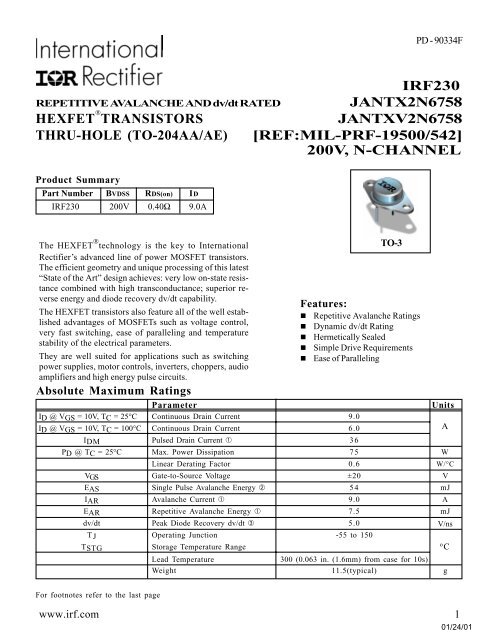
PD - 90334F<br />
REPETITIVE AVALANCHE AND dv/dt RATED JANTX<strong>2N6758</strong><br />
HEXFET ®<br />
TRANSISTORS JANTXV<strong>2N6758</strong><br />
THRU-HOLE (TO-204AA/AE) [REF:MIL-PRF-19500/542]<br />
200V, N-CHANNEL<br />
Product Summary<br />
Part Number BVDSS RDS(on) ID<br />
IRF230 200V 0.40Ω 9.0A<br />
The HEXFET ® technology is the key to <strong>International</strong><br />
<strong>Rectifier</strong>’s advanced line of power MOSFET transistors.<br />
The efficient geometry and unique processing of this latest<br />
“State of the Art” design achieves: very low on-state resistance<br />
combined with high transconductance; superior reverse<br />
energy and diode recovery dv/dt capability.<br />
The HEXFET transistors also feature all of the well established<br />
advantages of MOSFETs such as voltage control,<br />
very fast switching, ease of paralleling and temperature<br />
stability of the electrical parameters.<br />
They are well suited for applications such as switching<br />
power supplies, motor controls, inverters, choppers, audio<br />
amplifiers and high energy pulse circuits.<br />
PD @ TC = 25°C Max. Power Dissipation 75 W<br />
Linear Derating Factor 0.6 W/°C<br />
VGS Gate-to-Source Voltage ±20 V<br />
EAS Single Pulse Avalanche Energy ➁ 54 mJ<br />
IAR Avalanche Current ➀ 9.0 A<br />
EAR Repetitive Avalanche Energy ➀ 7.5 mJ<br />
dv/dt Peak Diode Recovery dv/dt ➂ 5.0 V/ns<br />
TJ Operating Junction -55 to 150<br />
TSTG<br />
Storage Temperature Range<br />
oC Lead Temperature 300 (0.063 in. (1.6mm) from case for 10s)<br />
Weight 11.5(typical) g<br />
For footnotes refer to the last page<br />
IRF230<br />
www.irf.com 1<br />
01/24/01<br />
TO-3<br />
Features:<br />
n Repetitive Avalanche Ratings<br />
n Dynamic dv/dt Rating<br />
n Hermetically Sealed<br />
n Simple Drive Requirements<br />
n Ease of Paralleling<br />
A
IRF230<br />
Electrical Characteristics @ Tj = 25°C (Unless Otherwise Specified)<br />
Parameter Min Typ Max Units Test Conditions<br />
BVDSS Drain-to-Source Breakdown Voltage 200 — — V VGS = 0V, ID = 1.0mA<br />
∆BVDSS/∆TJ Temperature Coefficient of Breakdown<br />
Voltage<br />
— 0.29 — V/°C Reference to 25°C, ID = 1.0mA<br />
RDS(on) Static Drain-to-Source On-State<br />
Resistance<br />
—<br />
—<br />
— 0.40 VGS = 10V, ID =6.0A➃<br />
Ω<br />
— 0.49 VGS =10V, ID =9.0A ➃<br />
VGS(th) Gate Threshold Voltage 2.0 — 4.0 V VDS = VGS, ID =250µA<br />
gfs Forward Transconductance 3.0 — — S ( ) VDS > 15V, IDS =6.0A➃<br />
IDSS Zero Gate Voltage Drain Current —<br />
—<br />
—<br />
—<br />
25<br />
250 µA<br />
VDS=160V, VGS=0V<br />
VDS =160V<br />
VGS = 0V, TJ = 125°C<br />
IGSS<br />
IGSS<br />
Gate-to-Source Leakage Forward<br />
Gate-to-Source Leakage Reverse<br />
—<br />
—<br />
—<br />
—<br />
100<br />
-100<br />
nA<br />
VGS =20V<br />
VGS =-20V<br />
Qg Total Gate Charge 16 — 39 VGS =10V, ID= 9.0A<br />
Qgs Gate-to-Source Charge 3.0 — 5.7 nC VDS =100V<br />
Qgd Gate-to-Drain (‘Miller’) Charge 8.0 — 20<br />
td(on) Turn-On Delay Time — — 35 VDD =100V, ID =9.0A,<br />
t r<br />
td(off)<br />
Rise Time<br />
Turn-Off Delay Time<br />
—<br />
—<br />
—<br />
—<br />
80<br />
60<br />
ns<br />
RG =7.5Ω<br />
tf Fall Time — — 40<br />
LS + LD Total Inductance — 6.1 — nH Measured from the center of<br />
drain pad to center of source<br />
pad<br />
Ciss Input Capacitance — 600 VGS = 0V, VDS =25V<br />
Coss Output Capacitance — 250 — pF f = 1.0MHz<br />
Crss Reverse Transfer Capacitance — 80 —<br />
Source-Drain Diode Ratings and Characteristics<br />
Parameter Min Typ Max Units Test Conditions<br />
IS Continuous Source Current (Body Diode) — — 9.0<br />
ISM Pulse Source Current (Body Diode) ➀ — — 36<br />
VSD Diode Forward Voltage — — 1.4 V Tj = 25°C, IS =9.0A, VGS = 0V ➃<br />
trr Reverse Recovery Time — — 500 nS Tj = 25°C, IF = 9.0A, di/dt ≤100A/µs<br />
QRR Reverse Recovery Charge — — 6.0 µc VDD ≤50V ➃<br />
ton Forward Turn-On Time Intrinsic turn-on time is negligible. Turn-on speed is substantially controlled by LS + LD.<br />
Thermal Resistance<br />
Parameter Min Typ Max Units Test Conditions<br />
RthJC Junction to Case — — 1.67<br />
°C/W<br />
RthJA Junction to Ambient — — 30 Typical socket mount<br />
2 www.irf.com<br />
A<br />
Ω
Fig 1. Typical Output Characteristics<br />
Fig 3. Typical Transfer Characteristics<br />
Fig 2. Typical Output Characteristics<br />
Fig 4. Normalized On-Resistance<br />
Vs. Temperature<br />
IRF230<br />
www.irf.com 3
IRF230<br />
Fig 5. Typical Capacitance Vs.<br />
Drain-to-Source Voltage<br />
Fig 7. Typical Source-Drain Diode<br />
Forward Voltage<br />
Fig 6. Typical Gate Charge Vs.<br />
Gate-to-Source Voltage<br />
13 a& b<br />
Fig 8. Maximum Safe Operating Area<br />
4 www.irf.com
Fig 9. Maximum Drain Current Vs.<br />
Case Temperature<br />
Fig 10a. Switching Time Test Circuit<br />
IRF230<br />
www.irf.com 5<br />
VDS 90%<br />
10%<br />
V GS<br />
R G<br />
V GS<br />
10V<br />
V DS<br />
Pulse Width ≤ 1 µs<br />
Duty Factor ≤ 0.1 %<br />
R D<br />
D.U.T.<br />
td(on) tr td(off) tf<br />
Fig 10b. Switching Time Waveforms<br />
Fig 11. Maximum Effective Transient Thermal Impedance, Junction-to-Case<br />
+<br />
-V DD
IRF230<br />
Fig 12a. Unclamped Inductive Test Circuit<br />
I AS<br />
10 V<br />
V G<br />
R G<br />
V DS<br />
20V 10V<br />
tp<br />
Q GS<br />
I AS<br />
tp<br />
Fig 12b. Unclamped Inductive Waveforms<br />
L<br />
D.U.T<br />
0.01Ω<br />
Q G<br />
Q GD<br />
Charge<br />
15V<br />
DRIVER<br />
V (BR)DSS<br />
Fig 13a. Basic Gate Charge Waveform<br />
+<br />
- VDD A<br />
Fig 12c. Maximum Avalanche Energy<br />
Vs. Drain Current<br />
6 www.irf.com<br />
12V<br />
V GS<br />
Current Regulator<br />
Same Type as D.U.T.<br />
.2µF<br />
50KΩ<br />
3mA<br />
.3µF<br />
D.U.T.<br />
IG ID Current Sampling Resistors<br />
+<br />
VDS -<br />
Fig 13b. Gate Charge Test Circuit
Foot Notes:<br />
➀ Repetitive Rating; Pulse width limited by<br />
maximum junction temperature.<br />
➁ VDD =50V, starting TJ = 25°C,<br />
➂ ISD ≤ 9.0A, di/dt ≤120A/µs,<br />
VDD≤ 200V, TJ ≤ 150°C<br />
Suggested RG =7.5 Ω<br />
Peak IL = 9.0A, ➃ Pulse width ≤ 300 µs; Duty Cycle ≤ 2%<br />
Case Outline and Dimensions —TO-204AA (Modified TO-3)<br />
IRF230<br />
IR WORLD HEADQUARTERS: 233 Kansas St., El Segundo, California 90245, USA Tel: (310) 252-7105<br />
IR EUROPEAN REGIONAL CENTRE: 439/445 Godstone Rd, Whyteleafe, Surrey CR3 OBL, UK Tel: ++ 44 (0)20 8645 8000<br />
IR CANADA: 15 Lincoln Court, Brampton, Ontario L6T3Z2, Tel: (905) 453 2200<br />
IR GERMANY: Saalburgstrasse 157, 61350 Bad Homburg Tel: ++ 49 (0) 6172 96590<br />
IR ITALY: Via Liguria 49, 10071 Borgaro, Torino Tel: ++ 39 011 451 0111<br />
IR JAPAN: K&H Bldg., 2F, 30-4 Nishi-Ikebukuro 3-Chome, Toshima-Ku, Tokyo 171 Tel: 81 (0)3 3983 0086<br />
IR SOUTHEAST ASIA: 1 Kim Seng Promenade, Great World City West Tower, 13-11, Singapore 237994 Tel: ++ 65 (0)838 4630<br />
IR TAIWAN:16 Fl. Suite D. 207, Sec. 2, Tun Haw South Road, Taipei, 10673 Tel: 886-(0)2 2377 9936<br />
Data and specifications subject to change without notice. 1/01<br />
www.irf.com 7