Internal Hardware Design of a Microcontroller in VLSI
Internal Hardware Design of a Microcontroller in VLSI
Internal Hardware Design of a Microcontroller in VLSI

You also want an ePaper? Increase the reach of your titles
YUMPU automatically turns print PDFs into web optimized ePapers that Google loves.
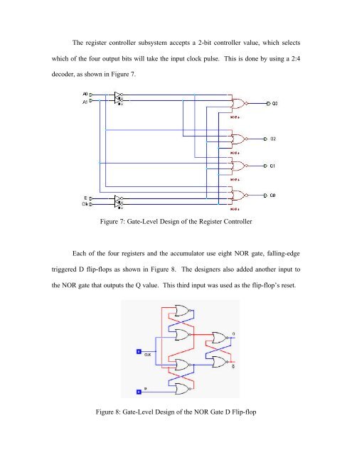
The register controller subsystem accepts a 2-bit controller value, which selects<br />
which <strong>of</strong> the four output bits will take the <strong>in</strong>put clock pulse. This is done by us<strong>in</strong>g a 2:4<br />
decoder, as shown <strong>in</strong> Figure 7.<br />
Figure 7: Gate-Level <strong>Design</strong> <strong>of</strong> the Register Controller<br />
Each <strong>of</strong> the four registers and the accumulator use eight NOR gate, fall<strong>in</strong>g-edge<br />
triggered D flip-flops as shown <strong>in</strong> Figure 8. The designers also added another <strong>in</strong>put to<br />
the NOR gate that outputs the Q value. This third <strong>in</strong>put was used as the flip-flop’s reset.<br />
Figure 8: Gate-Level <strong>Design</strong> <strong>of</strong> the NOR Gate D Flip-flop