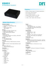
LP DK 790FX BIOS Setting Guideline - Dfi
LP DK 790FX BIOS Setting Guideline - Dfi
LP DK 790FX BIOS Setting Guideline - Dfi

Create successful ePaper yourself
Turn your PDF publications into a flip-book with our unique Google optimized e-Paper software.
<strong>LP</strong> <strong>DK</strong> <strong>790FX</strong> <strong>BIOS</strong> <strong>Setting</strong> <strong>Guideline</strong><br />
(<strong>BIOS</strong> version: 01/22/2008) V001<br />
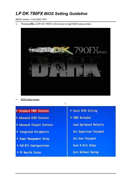
Pressing DEL at DFI <strong>DK</strong> <strong>790FX</strong> LOG screen to login <strong>BIOS</strong> setup screen<br />
<strong>BIOS</strong> setup screen<br />
L
Genie <strong>BIOS</strong> settings: This setup thread is combined all needed settings for over clocking<br />
(CPU speed setting, CPU features, DRAM timings, Voltage settings and PCI speed etc.)<br />
Genie <strong>BIOS</strong> : Main setup screen<br />
Timing Mode: Manual to control Memory Clock Value/Limit or AUTO by SPD detecting<br />
Memory Clock Value or Limit: 400~1066MHz; DRAM working ratio<br />
CPU Clock Ratio: 4/4.5~ 24.5x; CPU multiplier definition , by CPU type up to 24.5<br />
AMD K8 Cool&Quiet control: Enable/Disable AMD CPU advance power control function<br />
Spread Spectrum: Disable/Enable for reducing clock consumption<br />
CPU Host/HTT Cloock: 200~700MHz, CPU to NB bus working FSB<br />
CPU Host/HTT Boot Up Clock: 200~700MHz; First stage OC speed<br />
CPU Host/HTT Adjust Gap: 1~255 MHz; Frequency translating gap<br />
PCIE Clock: 100~250MHz; PCIE slot working frequency<br />
*CPU TLB Cache Fix: Enable /Disable TBL closed patch for Phenom DRAM controller<br />
*(Press F8 to boot for showing this item, Phenom CPU only)<br />
Onboard Devices :<br />
Onboard LAN1: Rear LAN1port controller, default AUTO (enabled)
DRAM Configuration :<br />
*DCTs Mode: DRAM controller definition; Ganged (dual controller) / Unganged (single controller)<br />
*item is for AMD Phenom CPU only<br />
MCT Memory Timing :<br />
This page is defining the DRAM signal strength for each Clock and Data bus, in order to work on higher<br />
working speed for tight DRAM timing.<br />
MCT Memory Timing: Auto by detecting SPD and Manual to adjust<br />
Maximum Latency: 1~15ns<br />
The maximum asynchronous latency is the maximum round-trip latency in the system from<br />
theprocessor to the DRAM devices and back. MaxAsyncLat is the sum of two components:<br />
1. The worst case delay setting for DqsRcvEnDelay<br />
2. A constant of 2ns associated with the delay internal to the processor
2T mode: Command rate mode 1T and 2T, Enable for 2T<br />
CAS latency Time (Tcl): 3~6 clocks; CAS (Column signal) latency time<br />
Precharge Delay (Tras): 5~18 Minimum timing of a command working cycle. (TRCD+CL+ 2 clock)<br />
DRAM RAS# Precharge (Trp) : 3~6 clock; Precharge timing for memory data by each command<br />
cycle<br />
DRAM RAS# To CAS# Delay (Trcd): 3~6 clock; RAS (Row signal) to CAS (Column signal) delay for<br />
read/write command<br />
Bank to Bank Delay (Trrd): 2~5 clocks; Command rate of memory's banks<br />
(Trc): 11~26 clocks; Minimum timing of a command to next command. (tRC) = (tRAS)+ (tRP)<br />
(Trtp): 2~5 clocks; Precharge period for read action<br />
(Twr): 3~6 clocks; Write recovery timing<br />
(Twtr): 1~3 clocks; delay write to read command for memory chips<br />
(Trfc0): 75~327ns; Minimum timing to reflash a ROW at same storage block(tRFC > tRC)-DIMM1 slot<br />
(Trfc1): DIMM 2 slot<br />
(Trfc2): DIMM 3 slot<br />
(Trfc3): DIMM 4 slot<br />
(Trdrd): 2~5 clocks<br />
(Trwrd): 3~9 clocks<br />
(Twrrd): 0~3 clocks<br />
(Twrwr):1~3 clocks<br />
CS/ODT Pin fine Delay: Enable /Disable DRAM terminal impedance/voltage optimized<br />
*TBL Cache mode: Enable /Disable TBL cache for Phenom DRAM controller<br />
Bank Swizzle Mode: Enable /Disable DRAM device Bank address bit remapping function<br />
AUTO Tweak Performance: Enable/Disable MCT optimized parameters<br />
Optimized performance mode: Enable/Disable<br />
Enable performance mode for DIMMS with peformance SPD. This provides an opportunity to<br />
adjust/scale or manually enter (from setup engine for example) controller; cycle times<br />
(CL,Trcd,Trp,Trtp,Tras.Trc,Twr.Trrd,Twtr,Tfrc(x))<br />
* item is for AMD Phenom CPU only
ODC control mode :<br />
DRAM Drive Weak/Normal mode: Weak/Normal; Memories data bus drive mode.<br />
Output Driver Comp: AUTO or Manual to adjust channel A/B drive strength abilities<br />
CPU On-Die Termination: 300/75/50 ohm OTD terminator resister definition<br />
DQS Drive Strength: 0.75 ~1.50x ; Memory data ready signal strength<br />
Data Drive Strength: 0.75 ~1.50x ; Memory data bus signal strength<br />
MEMCLK Drive Strength: 0.75 ~1.50x ; DRAM working clock signal strength<br />
Addr/Com Drive Strength: 1.0 ~2.0x ; DRAM address signal strength<br />
CS/ODT Drive Strength: 1.0 ~2.0x ; Memory modules BANK selection signals strength<br />
CKE Drive Strength: 1.0 ~2.0x ; Clock available signal strength<br />
CPU Feature: (Showing for Phenom CPU only )<br />
*CPU DID: 1~16;<br />
*CPU FID: 0000~003F; CPU COF = 100 MHz * (CpuFID + 10h) / CpuDID<br />
Ex: FID=0Ah, CPU DID=2<br />
CPU Speed= 100MHz *( 2Ch+10h)/2 ; 100MHz * (44+16)/2=100MHz * 30=3000MHz<br />
*CPU-NB DID: 1~2;<br />
*CPU-NB FID: 0000~001B NB COF = 200 MHz * ([NbFID + 4h / NbDID.<br />
*AMD CPU Stepping: P-states are operational performance states (states in which the processor is executing<br />
instructions, running software) characterized by a unique frequency and voltage. The processor supports up to 5
P-states called P-states 0 through 4 or P0 though P4. P0 is the highest power, highest<br />
performance P-state; each ascending P-state number represents a lower-power, lower<br />
performance P-state than the prior P-state number. At least one enabled P-state (P0) is<br />
specified for all processors.<br />
HT Link Control :<br />
HT Link Width: 16bit/8bit mode, CPU to NB bus hyper transfer bandwidth<br />
HT Link Frequency: 200~2600MHz (2.6GHz), CPU to NB bus hyper transfer speed<br />
IH Flow-Control Mode: Enable to support the use of the Isochronous Flow-Control Mode function to<br />
provide reduced latency for certain classes of southbridge traffic<br />
HT Link Tristate: Enable to tristate parts of the link in order to reduce power consumption. By default,<br />
no lanes are tristated. The CAD and CTL lanes may be tristated together or CAD, CTL, and CLK may<br />
be tristated.<br />
2X LCLK Mode: nil (will be removed by next version)<br />
UnitID Clumping: Enable to support UnitID clumping to increase the number of outstanding requests<br />
supported by a single device. It maybe enabled for PCI-Express GFX links in certain configurations.<br />
Clumping may be enabled when using only the lower number bridge within each PCI-Express GFX<br />
core<br />
PWM <strong>Setting</strong> :<br />
PWM Control: Enable/Disable to open Voltage control function<br />
CPU VID Special Add: plus on CPU voltage.
SB PLL 1.2V Voltage range: 1.20V~1.50V, South bridge working voltage.<br />
DRAM Voltage range: 1.8V~3.375V<br />
NB Core Voltage: 1.12V~1.50V, CPU to NB bus voltage<br />
NB PCIE Voltage: 1.12V~1.50V, CPU to NB bus voltage<br />
NB HT Voltage: 1.04V~1.50V, CPU to NB bus voltage<br />
PCIE Configuration: (Advance chipset feature)<br />
GPP Power Limit: 0~255W<br />
PCIE Slot1: First PCIE 16X slot configuration setting<br />
PCIE Slot2: Second PCIE 16X slot configuration setting<br />
PCIE Slot3: 3 rd PCIE 4X slot configuration setting<br />
NB-SB Port Feature: HT link configuration setting<br />
Gen2 High Speed Mode: Disable/software/Autonomous for PCI E Gen2 function<br />
Link ASPM: Disable/L0s/L1/L0s&L1;<br />
Link Width: 1~16X<br />
Slot Power Limit, W: 0~255W
<strong>BIOS</strong> Reloaded function: DFI Lan Party series are providing 1last fine status + 4 user’s profile<br />
space for doing <strong>BIOS</strong> setting saving and recovery.<br />
Auto Save bootable setting: Enable / Disable<br />
For saving last fine/ bootable parameters by <strong>BIOS</strong> itself every time<br />
Load last bootable:<br />
For loading last <strong>BIOS</strong> parameters.<br />
Save setting to bank with: Current settings or last saved CMOS settings.<br />
To define the resource of parameters for bank saving.<br />
User define setting bank #1 ~ #4:<br />
1. Bank Description: There are 4 rows for writing a short description. Double click on row when this<br />
row is empty, it will erase pervious data.<br />
2. Save to this bank: Press “Y” to save data to this bank<br />
3. Load from this bank: Press “Y” to load data of this bank to be current <strong>BIOS</strong> setup settings.<br />
4. Hotkey =>: define the “hotkey” for a quick change <strong>BIOS</strong> settings to boot. Please press Hotkey after<br />
power on system immediately.<br />
EZ Clear CMOS methods:<br />
a. EZ Clear Jumper
. To hold Home key to power on system, <strong>BIOS</strong> will recover FSB to default, remains setting will be<br />
keeping the last time fine status.<br />
c. To hold Insert key to power on system, <strong>BIOS</strong> will load all setting back to default as like doing a<br />
CCMOS by manually.<br />
End

![CP900-B [RoHS] - Dfi](https://img.yumpu.com/18888557/1/184x260/cp900-b-rohs-dfi.jpg?quality=85)
![CP900-B [RoHS] - Dfi](https://img.yumpu.com/18888555/1/184x260/cp900-b-rohs-dfi.jpg?quality=85)
![CP900-B [RoHS] - Dfi](https://img.yumpu.com/18888549/1/184x260/cp900-b-rohs-dfi.jpg?quality=85)
![CP900-B [RoHS] - Dfi](https://img.yumpu.com/18888536/1/184x260/cp900-b-rohs-dfi.jpg?quality=85)