AM-800600C3TMQW-TC0H - OLED-LCD-TFT
AM-800600C3TMQW-TC0H - OLED-LCD-TFT
AM-800600C3TMQW-TC0H - OLED-LCD-TFT

Create successful ePaper yourself
Turn your PDF publications into a flip-book with our unique Google optimized e-Paper software.
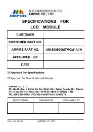
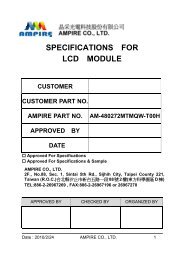
SPECIFICATIONS FOR<br />
<strong>LCD</strong> MODULE<br />
CUSTOMER<br />
CUSTOMER PART NO.<br />
<strong>AM</strong>PIRE PART NO. <strong>AM</strong>-<strong>800600C3TMQW</strong>-<strong>TC0H</strong><br />
APPROVED BY<br />
DATE<br />
Approved For Specifications<br />
Approved For Specifications & Sample<br />
<strong>AM</strong>PIRE CO., LTD.<br />
2F., No.88, Sec. 1, Sintai 5th Rd., Sijhih City, Taipei County 221,<br />
Taiwan (R.O.C.)台北縣汐止市新台五路一段 88 號 2 樓(東方科學園區 D 棟)<br />
TEL:886-2-26967269 , FAX:886-2-26967196 or 26967270<br />
APPROVED BY CHECKED BY ORGANIZED BY<br />
Date : 2009/06/23 <strong>AM</strong>PIRE CO., LTD. 1
RECORD OF REVISION<br />
Revision Date Page Contents Editor<br />
2009/06/23<br />
--<br />
New Release<br />
Emil<br />
Date : 2009/06/23 <strong>AM</strong>PIRE CO., LTD. 2
1. Features<br />
8 inch Amorphous-<strong>TFT</strong>-<strong>LCD</strong> (Thin Film Transistor Liquid Crystal Display) module.<br />
This module is composed of a 8” <strong>TFT</strong>-<strong>LCD</strong> panel, LED backlight, LED driver<br />
unit,touch panel and power circuit unit.<br />
(1) Construction: 8” a-Si <strong>TFT</strong> active matrix, White LED Backlight.<br />
(2) Resolution (pixel): 800(R.G.B) X600<br />
(3) Number of the Colors : 262K colors ( R , G , B 6 bit digital each)<br />
(4) <strong>LCD</strong> type : Transmissive , normally White<br />
(5) Interface: RGB interface 40 pin<br />
(6) Power Supply Voltage: 3.3V for logic voltage, 5.0V for LED driver power voltage.<br />
(7) Viewing Direction: 6 O’clock ( The direction it’s hard to be discolored )<br />
2. PHYSICAL SPECIFICATIONS<br />
Item Specifications unit<br />
<strong>LCD</strong> size 8 inch (Diagonal)<br />
Resolution 800 x 3(RGB) x 600 dot<br />
Dot pitch 0.0675(W) x 0.2025(H) mm<br />
Active area 162.0(W) x 121.5(H) mm<br />
Module size 183.0(W) x 141.0(H) x 10.58(D) mm<br />
Surface treatment Anti-Glare<br />
Color arrangement RGB-stripe<br />
interface Digital<br />
Weight T.B.D. g<br />
Date : 2009/06/23 <strong>AM</strong>PIRE CO., LTD. 3
3. ABSOLUTE MAX. RATINGS<br />
Item Symbol<br />
Power voltage<br />
Values<br />
Min. Max.<br />
VCC -0.3 4.6<br />
VLED -0.3 6.0<br />
UNIT Note<br />
Input signal voltage Vi -0.3 VCC+0.3 V Note 1<br />
Operation temperature TOP -20 70 ℃<br />
Storage temperature TST -30 80 ℃<br />
Note 1: The product is subject to be damaged permanently if stresses beyond<br />
those absolute maximum ratings listed above.<br />
Signals include : DCLK, DE, HS, VS, R0~R5, G0~G5, B0~B5.<br />
4. ELECTRICAL CHARACTERISTICS<br />
4-1 Typical Operation Conditions<br />
Values<br />
Item Symbol MIN TYP MAX Unit Remark<br />
Power Voltage VCC 3.0 3.3 3.6 V Note 1,2<br />
Power Consumption ICC -- 123 -- mA<br />
LED Driver Power<br />
Voltage<br />
LED Driver Current<br />
Consumption<br />
VLED 4.5 5.0 5.5 V<br />
ILED -- 410 -- mA<br />
Date : 2009/06/23 <strong>AM</strong>PIRE CO., LTD. 4<br />
V<br />
Note 1,2<br />
VCC=3.3V<br />
VLED=5V<br />
VADJ=3.3V<br />
(duty 100%)<br />
Input Voltage VIN 0 - VCC V<br />
Logic Logic input<br />
Input<br />
VTH 0.8VCC - VCC V Note 3<br />
high voltage<br />
Voltage Logic input<br />
VTL GND - 0.2VCC V Note 3<br />
low voltage<br />
Note 1: Value for Power Board combined panel.<br />
Note 2: VCC setting should match the signals output voltage (refer to Note 3) of<br />
customer’s system board.<br />
Note 3: DCLK, DE, HS, VS, R0~R5, G0~G5, B0~B5.
4-2 Backlight Driving Conditions<br />
Item Symbol<br />
Values<br />
Min. Typ. Max.<br />
Unit Note<br />
LED voltage VL 9.3 9.9 10.5 V Note 1<br />
LED current IL 162 180 198 mA Note 1<br />
LED life time -- 20,000 -- -- Hr Note 2<br />
Note 1 : The LED Supply Voltage is defined by the number of LED at Ta=25℃<br />
and IL=180mA.<br />
Note 2 : The “LED life time” is defined as the module brightness decrease to<br />
50% original brightness at Ta=25℃ and IL=180mA. The LED lifetime<br />
could be decreased if operating IL is larger than 180mA.<br />
Note 3 : When LCM is operated over 40℃ ambient temperature, the ILED should<br />
be follow :<br />
Date : 2009/06/23 <strong>AM</strong>PIRE CO., LTD. 5
4-3 Power Sequence<br />
Note : Data Signal includes DCLK, DE, HS, VS, R0~R5, G0~G5, B0~B5.<br />
Date : 2009/06/23 <strong>AM</strong>PIRE CO., LTD. 6
5. Optical Specifications<br />
Item Symbol Condition<br />
Viewing angle<br />
(CR≧10)<br />
Response time<br />
θL<br />
θR<br />
θT<br />
θB<br />
Φ = 180°<br />
(9 o’clock)<br />
Φ = 0°<br />
(3 o’clock)<br />
Φ = 90°<br />
(12 o’clock)<br />
Φ = 270°<br />
(6 o’clock)<br />
Values<br />
Min. Typ. Max.<br />
60 70 --<br />
60 70 --<br />
40 50 --<br />
60 70 --<br />
TON -- 10 20 msec<br />
TOFF -- 15 30 msec<br />
Unit Note<br />
degree Note1<br />
Date : 2009/06/23 <strong>AM</strong>PIRE CO., LTD. 7<br />
Note3<br />
Contrast ratio CR 400 500 -- -- Note4<br />
Color<br />
chromaticity<br />
WX<br />
Normal<br />
0.26 0.31 0.36 --<br />
θ=Φ=0°<br />
WY 0.28 0.33 0.38 --<br />
Note5<br />
Note6<br />
Luminance L 160 200 -- cd/㎡ Note6<br />
Luminance<br />
uniformity<br />
YU<br />
70 75 -- % Note7<br />
Test Conditions :<br />
1. VCC = 3.3V, IL = 180mA (Backlight current), the ambient temperature is<br />
25℃.<br />
2. The test systems refer to Note 2.
Note 1 : Definition of viewing angle range<br />
Note 2 : Definition of optical measurement system.<br />
The optical characteristics should be measured in dark room. After 30 minutes<br />
operation, the optical properties are measured at the center point of the <strong>LCD</strong> screen.<br />
(Response time is measured by Photo detector TOPCON BM-7, other items are<br />
measured by BM-5A/Field of view : 1° / Height : 500mm.)<br />
Date : 2009/06/23 <strong>AM</strong>PIRE CO., LTD. 8
Note 3 : Definition of Response time<br />
The response time is defined as the <strong>LCD</strong> optical switching time interval between<br />
“White” state and “Black” state. Rise time (TON) is the time between photo detector<br />
output intensity changed from 90% to 10%. And fall time (TOFF) is the time between<br />
photo detector output intensity changed from 10% to 90%.<br />
Note 4 : Definition of contrast ratio<br />
Luminance measured when <strong>LCD</strong> on the “White” state<br />
Contrast ratio (CR) =<br />
Luminance measured when <strong>LCD</strong> on the “Black” state<br />
Note 5 : Definition of color chromaticity (CIE1931)<br />
Color coordinated measured at center point of <strong>LCD</strong>.<br />
Note 6 : All input terminals <strong>LCD</strong> panel must be ground when measuring the center<br />
area of the panel.<br />
Date : 2009/06/23 <strong>AM</strong>PIRE CO., LTD. 9
Note 7 : Definition of Luminance Uniformity<br />
Active area is divided into 9 measuring areas (Refer to bellow figure). Every<br />
measuring point is placed at the center of each measuring area.<br />
Luminance Uniformity (Yu) =<br />
Bmin<br />
Bmax<br />
L ----- Active area length W ----- Active area width<br />
Bmax : The measured maximum luminance of all measurement position.<br />
Bmin : The measured minimum luminance of all measurement position.<br />
Date : 2009/06/23 <strong>AM</strong>PIRE CO., LTD. 10
6. INTERFACE<br />
<strong>TFT</strong> <strong>LCD</strong> Panel Driving Section<br />
Pin No. Symbol I/O Description Note<br />
1 VLED P Voltage for LED circuit (5.0V)<br />
2 VLED P Voltage for LED circuit (5.0V)<br />
3 ADJ I Adjust the LED brightness (1)<br />
4 GLED P Ground for LED circuit<br />
5 GLED P Ground for LED circuit<br />
6 VCC P Power supply for digital circuit (3.3V)<br />
7 VCC P Power supply for digital circuit (3.3V)<br />
8 MODE I DE or SYNC mode control (2)<br />
9 DE I Data enable<br />
10 VSYNC I VSYNC signal input<br />
11 HSYNC I HSYNC signal input<br />
12 GND P Power ground<br />
13 B5 I Blue data input (MSB)<br />
14 B4 I Blue data input<br />
15 B3 I Blue data input<br />
16 GND P Power ground<br />
17 B2 I Blue data input<br />
18 B1 I Blue data input<br />
19 B0 I Blue data input (LSB)<br />
20 GND P Power ground<br />
21 G5 I Green data input (MSB)<br />
22 G4 I Green data input<br />
23 G3 I Green data input<br />
24 GND P Power ground<br />
25 G2 I Green data input<br />
Date : 2009/06/23 <strong>AM</strong>PIRE CO., LTD. 11
26 G1 I Green data input<br />
27 G0 I Green data input (LSB)<br />
28 GND P Power ground<br />
29 R5 I Red data input (MSB)<br />
30 R4 I Red data input<br />
31 R3 I Red data input<br />
32 GND P Power ground<br />
33 R2 I Red data input<br />
34 R1 I Red data input<br />
35 R0 I Red data input (LSB)<br />
36 GND P Power ground<br />
37 DCLK I Sample clock<br />
38 GND P Power ground<br />
39 L/R I Select left to right scanning direction (3)<br />
40 U/D I Select up or down scanning direction (3)<br />
I : input, O : output, P : power<br />
Date : 2009/06/23 <strong>AM</strong>PIRE CO., LTD. 12
NOTE :<br />
(1) Pin3: ADJ is PWM signal input. It is for brightness control.<br />
ITEM SYMBOL MIN TYP MAX UNIT<br />
ADJ signal frequency fPWM 100 -- 1K Hz<br />
ADJ signal logic level High VIH 2V --<br />
VLED<br />
(5.0V)<br />
V<br />
ADJ signal logic level Low VIL 0 -- 0.5 V<br />
(2) DE Mode, Mode=”H”,HSYNC floating and VSYNC floating<br />
HV Mode, Mode=”L” and DE floating<br />
(3) Selection of scanning mode<br />
Setting of scan<br />
control input<br />
Scanning direction<br />
U/D R/L<br />
GND VCC Up to Down, Left to Right<br />
VCC GND Down to Up, Right to Left<br />
GND GND Up to Down, Right to Left<br />
VCC VCC Down to Up, Left to Right<br />
Date : 2009/06/23 <strong>AM</strong>PIRE CO., LTD. 13
7. INPUT SIGNAL :<br />
7-1 AC Electrical Characteristics<br />
Date : 2009/06/23 <strong>AM</strong>PIRE CO., LTD. 14
7-2 Timing<br />
7-3 Input Clock and Data Timing Diagram<br />
Date : 2009/06/23 <strong>AM</strong>PIRE CO., LTD. 15
8. RELIABILITY TEST CONDITIONS<br />
(Note 3)<br />
Item Test Conditions Note<br />
High Temperature Storage Ta = 80℃ 240 hrs Note 1,4<br />
Low Temperature Storage Ta = -30℃ 240 hrs Note 1,4<br />
High Temperature Operation Ts = 70℃ 240 hrs Note 2,4<br />
Low Temperature Operation Ta = -20℃ 240 hrs Note1,4<br />
Operate at High Temperature<br />
and Humidity<br />
Thermal Shock<br />
Vibration Test<br />
Mechanical Shock<br />
Package Vibration Test<br />
Package Drop Test<br />
+40℃, 90%RH 240 hrs<br />
-30℃ /30 min ~ +80℃ /30 min for a total 100<br />
cycles, Start with cold temperature and end<br />
with high temperature<br />
Frequency range : 10 ~ 55Hz<br />
Stroke : 1.5mm<br />
Sweep : 10Hz ~ 55Hz ~ 10Hz<br />
2 hours for each direction of X. Y. Z.<br />
(6 hours for total)<br />
100G 6ms, ±X, ±Y, ±Z 3 times for each<br />
direction<br />
Random Vibration :<br />
0.015G*G/Hz from 5-200HZ, -6dB/Octave<br />
from 200-500Hz<br />
2 hours for each direction of X. Y. Z.<br />
(6 hours for total)<br />
Height : 60 cm<br />
1 comer, 3 edges, 6 surfaces<br />
Electro Static Discharge ±2KV, Human Body Mode, 100pF/1500Ω<br />
Note 1 : Ta is the ambient temperature of samples.<br />
Note 2 : Ts is the temperature of panel’s surface.<br />
Note 3 : In the standard condition, there shall be no practical problem that may affect<br />
the display function. After the reliability test, the product only guarantees<br />
operation, but don’t guarantee all of the cosmetic specification.<br />
Note 4 : Before cosmetic and function test, the product must have enough recovery<br />
time, at least 2 hours at room temperature.<br />
Date : 2009/06/23 <strong>AM</strong>PIRE CO., LTD. 16
Display Quality<br />
1. Function Related :<br />
The function defects of line defect, abnormal display, and no display are<br />
considered Major defects.<br />
2. Bright / Dark Dots :<br />
Note : The definition of dot : The size of a defective dot over 1/2 of whole dot is<br />
regarded as one defective dot.<br />
Bright dot : Dots appear bright and unchanged in size in which <strong>LCD</strong><br />
panel is displaying under black pattern.<br />
Dark dot : Dots appear dark and unchanged in size in which <strong>LCD</strong> panel<br />
is displaying under pure red, green, blue pattern.<br />
3. Pixel Definition :<br />
Defect Type Specification Major Minor<br />
Bright Dots N
9. General Precautions<br />
9-1 Safety<br />
Liquid crystal is poisonous. Do not put it your month. If liquid crystal touches<br />
your skin or clothes, wash it off immediately by using soap and water.<br />
9-2 Handling<br />
1. The <strong>LCD</strong> panel is plate glass. Do not subject the panel to mechanical<br />
shock or to excessive force on its surface.<br />
2. The polarizer attached to the display is easily damaged. Please handle it<br />
carefully to avoid scratch or other damages.<br />
3. To avoid contamination on the display surface, do not touch the module<br />
surface with bare hands.<br />
4. Keep a space so that the <strong>LCD</strong> panels do not touch other components.<br />
5. Put cover board such as acrylic board on the surface of <strong>LCD</strong> panel to<br />
protect panel from damages.<br />
6. Transparent electrodes may be disconnected if you use the <strong>LCD</strong> panel<br />
under environmental conditions where the condensation of dew occurs.<br />
7. Do not leave module in direct sunlight to avoid malfunction of the ICs.<br />
9-3 Static Electricity<br />
1. Be sure to ground module before turning on power or operation module.<br />
2. Do not apply voltage which exceeds the absolute maximum rating value.<br />
9-4 Storage<br />
1. Store the module in a dark room where must keep at +25±10℃ and<br />
65%RH or less.<br />
2. Do not store the module in surroundings containing organic solvent or<br />
corrosive gas.<br />
3. Store the module in an anti-electrostatic container or bag.<br />
9-5 Cleaning<br />
1. Do not wipe the polarizer with dry cloth. It might cause scratch.<br />
2. Only use a soft sloth with IPA to wipe the polarizer, other chemicals might<br />
permanent damage to the polarizer.<br />
9-5 Others<br />
1. <strong>AM</strong>IPRE will provide one year warrantee for all products and three months<br />
warrantee for all repairing products.<br />
Date : 2009/06/23 <strong>AM</strong>PIRE CO., LTD. 18
10. OUTLINE DIMENSION<br />
Date : 2009/06/23 <strong>AM</strong>PIRE CO., LTD. 19