AM-800600J1TMQW-TA0H - Displays: OLED-LCD-TFT
AM-800600J1TMQW-TA0H - Displays: OLED-LCD-TFT
AM-800600J1TMQW-TA0H - Displays: OLED-LCD-TFT

You also want an ePaper? Increase the reach of your titles
YUMPU automatically turns print PDFs into web optimized ePapers that Google loves.
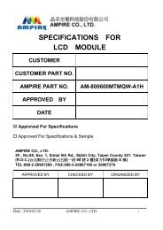
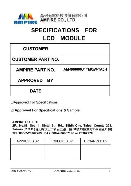
SPECIFICATIONS FOR<br />
<strong>LCD</strong> MODULE<br />
CUSTOMER<br />
CUSTOMER PART NO.<br />
<strong>AM</strong>PIRE PART NO.<br />
APPROVED BY<br />
DATE<br />
Approved For Specifications<br />
Approved For Specifications & Sample<br />
<strong>AM</strong>-<strong>800600J1TMQW</strong>-<strong>TA0H</strong><br />
<strong>AM</strong>PIRE CO., LTD.<br />
2F., No.88, Sec. 1, Sintai 5th Rd., Sijhih City, Taipei County 221,<br />
Taiwan (R.O.C.)台北縣汐止市新台五路一段 88 號 2 樓(東方科學園區 D 棟)<br />
TEL:886-2-26967269 , FAX:886-2-26967196 or 26967270<br />
APPROVED BY CHECKED BY ORGANIZED BY<br />
Date : 2009/07/21 <strong>AM</strong>PIRE CO., LTD. 1
RECORD OF REVISION<br />
Revision Date Page Contents Editor<br />
2009/07/02<br />
2009/7/21<br />
-<br />
-<br />
New Release<br />
Revise all T.B.D value<br />
Emil<br />
John<br />
Date : 2009/07/21 <strong>AM</strong>PIRE CO., LTD. 2
1. INSTRUCTION<br />
Ampire 7” Display Module is a color active matrix <strong>TFT</strong>-<strong>LCD</strong> that uses amorphous silicon<br />
<strong>TFT</strong> as a switching device . This model is composed of a <strong>TFT</strong>-<strong>LCD</strong> panel , a driving<br />
circuit ,touch panel. This <strong>TFT</strong>-<strong>LCD</strong> has a high resolution (800(R.G.B) X 600) and can<br />
display up to 262,144 colors.<br />
1.1 Features<br />
(1) Construction : a-Si <strong>TFT</strong>-<strong>LCD</strong> with driving system, White LED Backlight, touch panel.<br />
(2) <strong>LCD</strong> type : Transmissive , Normally White<br />
(3) Number of the Colors : 262K colors (R,G,B 6 bit digital each)<br />
(4) LVDS Interface.<br />
(5) <strong>LCD</strong> Power Supply Voltage : 3.3V single power input, built-in power supply circuit.<br />
● SVGA (4:3 diagonal) configuration<br />
● Input interface voltage : 3.3V<br />
2. PHYSICAL SPECIFICATIONS<br />
Item Specifications unit<br />
Display resolution(dot) 800RGB (W) x 600(H) dots<br />
Active area 141.60 (W) x 106.20 (H) mm<br />
Pixel pitch 59 (W) x 177 (H) um<br />
Color configuration R.G.B -stripe<br />
Overall dimension 154(W)x119.2(H)x10.2(D). mm<br />
Weight 206 g<br />
Brightness 400nit cd/m 2<br />
Contrast ratio 250<br />
Backlight unit LED<br />
Display color 262,144 colors<br />
Date : 2009/07/21 <strong>AM</strong>PIRE CO., LTD. 3
3. ABSOLUTE MAXIMUM RATINGS<br />
Item Symbol Min. Max. Unit Note<br />
Supply voltage range VCC -0.5 4 V (1)<br />
Voltage range at any terminal VI -0.5 VCC + 0.5 V<br />
Operating Temperature Top -10 70 ℃<br />
Storage Temperature Tstg -20 80 ℃<br />
(1)All voltage values are with respect to the GND terminals unless otherwise noted.<br />
4. OPTICAL CHARACTERISTICS<br />
Item Symbol Conditon Min. Typ. Max. Unit Note<br />
Response Time Tr +Tf - 16 -- ms (1)<br />
Θ=Φ=0°<br />
Contrast ratio CR<br />
-- 250 - - (2)(3)<br />
Viewing Vertical Θ -- 120 -<br />
CR≧ 10<br />
Angle Horizontal Φ<br />
-- 140 -<br />
Deg. (5)<br />
Luminance L -- 400 - cd/m 2 (3)(4)<br />
Luminance Uniformity ΔL - 70 - % (3)(4)<br />
Color<br />
chromaticity<br />
Wx 0.26 0.32 0.38<br />
White<br />
Θ=Φ=0°<br />
Wy<br />
0.27 0.33 0.39<br />
NOTE :<br />
● These items are measured by BM-5A(TOPCON) or CA-1000(MINOLTA) in the dark<br />
room (no ambient light)<br />
●T.B.D means To be define.<br />
(1) Definition of Response Time (White-Black)<br />
Date : 2009/07/21 <strong>AM</strong>PIRE CO., LTD. 4
(2) Definition of Contrast Ratio<br />
Measure contrast ratio on the below 5 points(refer to figurel,#1~#5point) and take<br />
the average value<br />
Contrast ratio is calculated with the following formula :<br />
Contrast Ratio(CR)=(White)Luminance of ON ÷ (Black)Luminance of OFF<br />
(3) Definition of Luminance :<br />
Measured at the center area of the panel when all the input terminals of <strong>LCD</strong> panel<br />
are electrically opened.<br />
(4)Definition of Luminance Uniformity :<br />
Measured Maximum luminance[L(MAX)] and Minimum luminance[L(MIN)] on the 5<br />
points<br />
Luminance Uniformity is calculated with the following formula :<br />
ΔL =[ L(MIN) / L (MAX) ] X 100%<br />
(5)Definition of Viewing Angle<br />
Φ =(Θx+)+(Θx-) Θ =(Θy+)+(Θy-)<br />
Date : 2009/07/21 <strong>AM</strong>PIRE CO., LTD. 5
5. ELECTRICAL CHARACTERISTICS<br />
Date : 2009/07/21 <strong>AM</strong>PIRE CO., LTD. 6
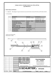
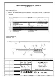
5.1 Touch Panel Electrical Specification<br />
Parameter Condition Standard Value<br />
Terminal Resistance<br />
X Axis<br />
Y Axis<br />
200~ 900 Ω<br />
100 ~ 640 Ω<br />
Insulating Resistance DC 25 V More than 20MΩ<br />
Linearity -- ±1.5 %<br />
Pen writing Durability Note a 100,000 times(min)<br />
Input life by finger Note b 1,000,000 times (min)<br />
Note A .<br />
Writing length 35 mm.<br />
Writing speed: 300mm/sec.<br />
Shape of pen end : R0.8<br />
Load : 250 g<br />
Note B<br />
By Silicon rubber tapping at same point<br />
Shape of rubber end: R8<br />
Load: 200g<br />
Frequency: 5 Hz<br />
Interface<br />
No. Symbol Function<br />
1 XL Touch Panel Left Signal<br />
2 YD Touch Panel Bottom Signal<br />
3 XR Touch Panel Right Signal<br />
4 YU Touch Panel Top Signal<br />
6. Backlight unit<br />
ITEM SYMBOL MIN TYP MAX UNIT NOTE<br />
LED Voltage VL -- 10.4 -- V<br />
LED Current IL -- 200 -- mA<br />
Luminance L -- 400 -- cd/m 2<br />
Date : 2009/07/21 <strong>AM</strong>PIRE CO., LTD. 7
7. INTERFACE<br />
LVDS CN:<br />
Pin no Symbol Function<br />
1 VDD POWER SUPPLY:3.3V<br />
2 VDD POWER SUPPLY:3.3V<br />
3 Gnd Power Ground<br />
4 Gnd Power Ground<br />
5 IN0- Transmission Data<br />
6 IN0+ Transmission Data<br />
7 Gnd Power Ground<br />
8 IN1- Transmission Data<br />
9 IN1+ Transmission Data<br />
10 Gnd Power Ground<br />
11 IN2- Transmission Data<br />
12 IN2+ Transmission Data<br />
13 Gnd Power Ground<br />
14 CLK- Sampling Clock<br />
15 CLK+ Sampling Clock<br />
16 Gnd Power Ground<br />
17 NC No Connect<br />
18 NC No Connect<br />
19 Gnd Power Ground<br />
20 Gnd Power Ground<br />
Date : 2009/07/21 <strong>AM</strong>PIRE CO., LTD. 8
8. AC Timing characteristic of the LVDS<br />
Date : 2009/07/21 <strong>AM</strong>PIRE CO., LTD. 9
Date : 2009/07/21 <strong>AM</strong>PIRE CO., LTD. 10
9 . QUALITY AND RELIABILITY<br />
9.1 TEST CONDITIONS<br />
Tests should be conducted under the following conditions :<br />
Ambient temperature : 25 ± 5°C<br />
Humidity : 60 ± 25% RH.<br />
9.2 S<strong>AM</strong>PLING PLAN<br />
Sampling method shall be in accordance with MIL-STD-105E , level II, normal<br />
single sampling plan .<br />
9.3 ACCEPTABLE QUALITY LEVEL<br />
A major defect is defined as one that could cause failure to or materially reduce<br />
the usability of the unit for its intended purpose. A minor defect is one that does not<br />
materially reduce the usability of the unit for its intended purpose or is an infringement from<br />
established standards and has no significant bearing on its effective use or operation.<br />
9.4 APPEARANCE<br />
An appearance test should be conducted by human sight at approximately 30 cm<br />
distance from the <strong>LCD</strong> module under florescent light. The inspection area of <strong>LCD</strong> panel<br />
shall be within the range of following limits.<br />
Date : 2009/07/21 <strong>AM</strong>PIRE CO., LTD. 11
9.5 INCOMING INSPECTION STANDARD FOR <strong>TFT</strong>-<strong>LCD</strong> PANEL<br />
VISUAL<br />
DEFECT<br />
ELECTRICAL<br />
DEFECT<br />
DEFECT TYPE LIMIT<br />
INTERNAL<br />
SPOT<br />
FIBER<br />
POLARIZER<br />
BUBBLE<br />
Mura<br />
BRIGHT DOT<br />
φ
[Note3]<br />
C Area: Center of display area<br />
C Area: Outer of display area<br />
[Note4]<br />
Judge defect dot and adjacent dot as following. Allow below (as A, B, C and D status)<br />
adjacent defect dots, including bright and dart adjacent dot. And they will be counted 2<br />
defect dots in total quantity.<br />
(1) The defects that are not defined above and considered to be problem shall be reviewed<br />
and discussed by both parties.<br />
(2) Defects on the Black Matrix, out of Display area, are not considered as a defect or counted.<br />
Date : 2009/07/21 <strong>AM</strong>PIRE CO., LTD. 13
9.6 Reliability Test<br />
Test Item Test Conditions Note<br />
High Temperature Operation 70±3°C , t=96 hrs<br />
Low Temperature Operation -10±3°C , t=96 hrs<br />
High Temperature Storage 80±3°C , t=96 hrs 1,2<br />
Low Temperature Storage -20±3°C , t=96 hrs 1,2<br />
Thermal Shock Test<br />
-10°C ~ 25°C ~ 70°C<br />
30 m in. 5 min. 30 min. ( 1 cycle )<br />
Total 5 cycle<br />
Humidity Test 40 °C, Humidity 90%, 96 hrs 1,2<br />
Sweep frequency : 10 ~ 55 ~ 10 Hz/1min<br />
Amplitude : 0.75mm<br />
Vibration Test (Packing)<br />
Test direction : X.Y.Z/3 axis<br />
Duration : 30min/each axis<br />
Note 1 : Condensation of water is not permitted on the module.<br />
Note 2 : The module should be inspected after 1 hour storage in normal conditions<br />
(15-35°C , 45-65%RH).<br />
Definitions of life end point :<br />
Current drain should be smaller than the specific value.<br />
Function of the module should be maintained.<br />
Appearance and display quality should not have degraded noticeably.<br />
Contrast ratio should be greater than 50% of the initial value.<br />
Date : 2009/07/21 <strong>AM</strong>PIRE CO., LTD. 14<br />
1,2<br />
2
10. USE PRECAUTIONS<br />
10.1 Handling precautions<br />
1) The polarizing plate may break easily so be careful when handling it. Do not touch,<br />
press or rub it with a hard-material tool like tweezers.<br />
2) Do not touch the polarizing plate surface with bare hands so as not to make it dirty. If<br />
the surface or other related part of the polarizing plate is dirty, soak a soft cotton cloth or<br />
chamois leather in benzine and wipe off with it. Do not use chemical liquids such as<br />
acetone, toluene and isopropyl alcohol. Failure to do so may bring chemical reaction<br />
phenomena and deteriorations.<br />
3) Remove any spit or water immediately. If it is left for hours, the suffered part may deform<br />
or decolorize.<br />
4) If the <strong>LCD</strong> element breaks and any LC stuff leaks, do not suck or lick it. Also if LC stuff is stuck<br />
on your skin or clothing, wash thoroughly with soap and water immediately.<br />
10.2 Installing precautions<br />
1) The PCB has many ICs that may be damaged easily by static electricity. To prevent<br />
breaking by static electricity from the human body and clothing, earth the human body<br />
properly using the high resistance and discharge static electricity during the operation.<br />
In this case, however, the resistance value should be approx. 1MΩ and the resistance<br />
should be placed near the human body rather than the ground surface. When the indoor<br />
space is dry, static electricity may occur easily so be careful. We recommend the indoor<br />
space should be kept with humidity of 60% or more. When a soldering iron or other<br />
similar tool is used for assembly, be sure to earth it.<br />
2) When installing the module and ICs, do not bend or twist them. Failure to do so may<br />
crack LC element and cause circuit failure.<br />
3) To protect LC element, especially polarizing plate, use a transparent protective plate<br />
(e.g., acrylic plate, glass etc) for the product case.<br />
4) Do not use an adhesive like a both-side adhesive tape to make <strong>LCD</strong> surface (polarizing<br />
plate) and product case stick together. Failure to do so may cause the polarizing plate to<br />
peel off.<br />
10.3 Storage precautions<br />
1) Avoid a high temperature and humidity area. Keep the temperature between 0°C and<br />
35°C and also the humidity under 60%.<br />
2) Choose the dark spaces where the product is not exposed to direct sunlight or<br />
fluorescent light.<br />
3) Store the products as they are put in the boxes provided from us or in the same<br />
conditions as we recommend.<br />
Date : 2009/07/21 <strong>AM</strong>PIRE CO., LTD. 15
10.4 Operating precautions<br />
1) Do not boost the applied drive voltage abnormally. Failure to do so may break ICs.<br />
When applying power voltage, check the electrical features beforehand and be careful.<br />
Always turn off the power to the LC module controller before removing or inserting the<br />
LC module input connector. If the input connector is removed or inserted while the<br />
power is turned on, the LC module internal circuit may break.<br />
2) The display response may be late if the operating temperature is under the normal<br />
standard, and the display may be out of order if it is above the normal standard. But this<br />
is not a failure; this will be restored if it is within the normal standard.<br />
3) The <strong>LCD</strong> contrast varies depending on the visual angle, ambient temperature, power<br />
voltage etc. Obtain the optimum contrast by adjusting the LC dive voltage.<br />
4) When carrying out the test, do not take the module out of the low-temperature space<br />
suddenly. Failure to do so will cause the module condensing, leading to malfunctions.<br />
5) Make certain that each signal noise level is within the standard (L level: 0.2Vdd or less<br />
and H level: 0.8Vdd or more) even if the module has functioned properly. If it is beyond<br />
the standard, the module may often malfunction. In addition, always connect the module<br />
when making noise level measurements.<br />
6) The CMOS ICs are incorporated in the module and the pull-up and pull-down function is<br />
not adopted for the input so avoid putting the input signal open while the power is ON.<br />
7) The characteristic of the semiconductor element changes when it is exposed to light<br />
emissions, therefore ICs on the <strong>LCD</strong> may malfunction if they receive light emissions. To<br />
prevent these malfunctions, design and assemble ICs so that they are shielded from<br />
light emissions.<br />
8) Crosstalk occurs because of characteristics of the <strong>LCD</strong>. In general, crosstalk occurs<br />
when the regularized display is maintained. Also, crosstalk is affected by the LC drive<br />
voltage. Design the contents of the display, considering crosstalk.<br />
10.5 Other<br />
1) Do not disassemble or take the LC module into pieces. The LC modules once<br />
disassembled or taken into pieces are not the guarantee articles.<br />
2) The residual image may exist if the same display pattern is shown for hours. This<br />
residual image, however, disappears when another display pattern is shown or the drive<br />
is interrupted and left for a while. But this is not a problem on reliability.<br />
3) <strong>AM</strong>IPRE will provide one year warranty for all products and three months warrantee for<br />
all repairing products.<br />
Date : 2009/07/21 <strong>AM</strong>PIRE CO., LTD. 16
11. OUTLINE DIMENSION<br />
Date : 2009/07/21 <strong>AM</strong>PIRE CO., LTD. 17