InP-based polarisation independent wavelength demultiplexers
InP-based polarisation independent wavelength demultiplexers
InP-based polarisation independent wavelength demultiplexers

Create successful ePaper yourself
Turn your PDF publications into a flip-book with our unique Google optimized e-Paper software.
2.3 Applications 29<br />
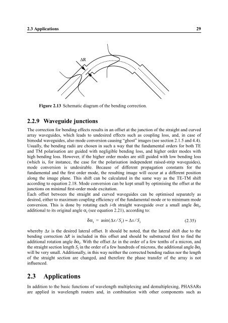
2.2.9 Waveguide junctions<br />
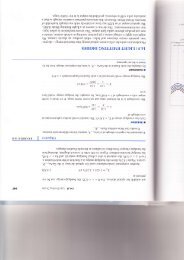
The correction for bending effects results in an offset at the junction of the straight and curved<br />
array waveguides, which leads to undesired effects such as coupling loss, and, in case of<br />
bimodal waveguides, also mode conversion causing “ghost” images (see section 2.1.5 and 4.4).<br />
Usually, the bending radii are chosen in such a way that the fundamental orders for both TE<br />
and TM <strong>polarisation</strong> are guided with negligible bending loss, and higher order modes with<br />
high bending loss. However, if the higher order modes are still guided with low bending loss<br />
(which is, for instance, the case for the <strong>polarisation</strong> <strong>independent</strong> raised-strip waveguides),<br />
mode conversion is undesirable. Because of different propagation constants for the<br />
fundamental and the first order mode, the resulting image will occur at a different position<br />
along the image plane. This shift can be calculated in the same way as the TE-TM shift<br />
according to equation 2.18. Mode conversion can be kept small by optimising the offset at the<br />
junctions on minimal first-order mode excitation.<br />
Each offset between the straight and curved waveguides can be optimised separately as<br />
desired, either to maximum coupling efficiency of the fundamental mode or to minimum mode<br />
conversion. This is done by rotating each i-th straight waveguide over a small angle δα i ,<br />
additional to its original angle α i (see equation 2.21), according to:<br />
whereby Δx is the desired lateral offset. It should be noted, that the lateral shift due to the<br />
bending correction ΔR is included in this offset and should be substracted first to find the<br />
additional rotation angle δα i . With the offset Δx in the order of a few tenths of a micron, and<br />
the straight section length S i in the order of a few hundreds of microns, the additional angle δα i<br />
will be very small. Additionally, in this way neither the corrected bending radius nor the length<br />
of the straight section are changed, and therefore the phase transfer of the array is not<br />
influenced.<br />
2.3 Applications<br />
ΔR<br />
Figure 2.13 Schematic diagram of the bending correction.<br />
δα i<br />
= asin( Δx ⁄ Si) ≈ Δx ⁄ Si (2.35)<br />
In addition to the basic functions of <strong>wavelength</strong> multiplexing and demultiplexing, PHASARs<br />
are applied in <strong>wavelength</strong> routers and, in combination with other components such as