InP-based polarisation independent wavelength demultiplexers
InP-based polarisation independent wavelength demultiplexers
InP-based polarisation independent wavelength demultiplexers

You also want an ePaper? Increase the reach of your titles
YUMPU automatically turns print PDFs into web optimized ePapers that Google loves.
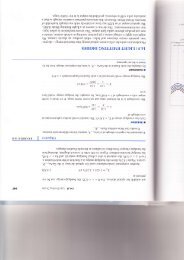
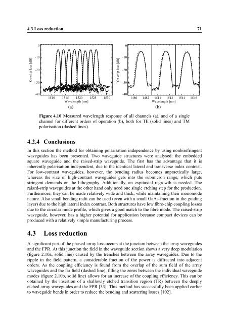
4.3 Loss reduction 71<br />
On-chip loss [dB]<br />
0<br />
-10<br />
-20<br />
-30<br />
-40<br />
1510 1515 1520 1525 1530<br />
Wavelength [nm]<br />
4.2.4 Conclusions<br />
In this section the method for obtaining <strong>polarisation</strong> independence by using nonbirefringent<br />
waveguides has been presented. Two waveguide structures were analysed: the embedded<br />
square waveguide and the raised-strip waveguide. The first has the advantage that it is<br />
inherently <strong>polarisation</strong> <strong>independent</strong>, due to the identical lateral and transverse index contrast.<br />
For low-contrast waveguides, however, the bending radius becomes unpractically large,<br />
whereas the size of high-contrast waveguides gets into the submicron range, which puts<br />
stringent demands on the lithography. Additionally, an expitaxial regrowth is needed. The<br />
raised-strip waveguides at the other hand only need one single etching step for the production.<br />
Furthermore, they can be made relatively wide and thick, while maintaining their monomode<br />
nature. Also small bending radii can be used (even with a small GaAs-fraction in the guiding<br />
layer) due to the high lateral index contrast. Both structures have low fibre-chip coupling losses<br />
due to the circular mode profile, which gives a good match to the fibre mode. The raised-strip<br />
waveguide, however, has a higher potential for application because compact devices can be<br />
produced with a relatively simple manufacturing process.<br />
4.3 Loss reduction<br />
(a) (b)<br />
A significant part of the phased-array loss occurs at the junction between the array waveguides<br />
and the FPR. At this junction the field in the waveguide section shows a very deep modulation<br />
(figure 2.10a, solid line) caused by the trenches between the array waveguides. Due to the<br />
ripple in the field pattern, a considerable fraction of the power is diffracted into adjacent<br />
orders. As the coupling efficiency is found from the overlap of the sum field of the array<br />
waveguides and the far field (dashed line), filling the zeros between the individual waveguide<br />
modes (figure 2.10b, solid line) allows for an increase of the coupling efficiency. This can be<br />
obtained by the insertion of a shallowly etched transition region (TR) between the deeply<br />
etched array waveguides and the FPR [33]. This method has successfully been applied earlier<br />
to waveguide bends in order to reduce the bending and scattering losses [102].<br />
On-chip loss [dB]<br />
0<br />
-10<br />
-20<br />
-30<br />
-40<br />
1480 1482 1511 1513<br />
Wavelength [nm]<br />
1544 1546<br />
Figure 4.10 Measured <strong>wavelength</strong> response of all channels (a), and of a single<br />
channel for different orders of operation (b), both for TE (solid lines) and TM<br />
<strong>polarisation</strong> (dashed lines).