InP-based polarisation independent wavelength demultiplexers
InP-based polarisation independent wavelength demultiplexers
InP-based polarisation independent wavelength demultiplexers

Create successful ePaper yourself
Turn your PDF publications into a flip-book with our unique Google optimized e-Paper software.
5.2 Polarisation dispersion compensation 87<br />
processing, this method appeals to the controllability of the production process and to the skills<br />
of the persons who actually manufacture the devices.<br />
<strong>InP</strong> layer thickness [nm]<br />
400<br />
350<br />
300<br />
250<br />
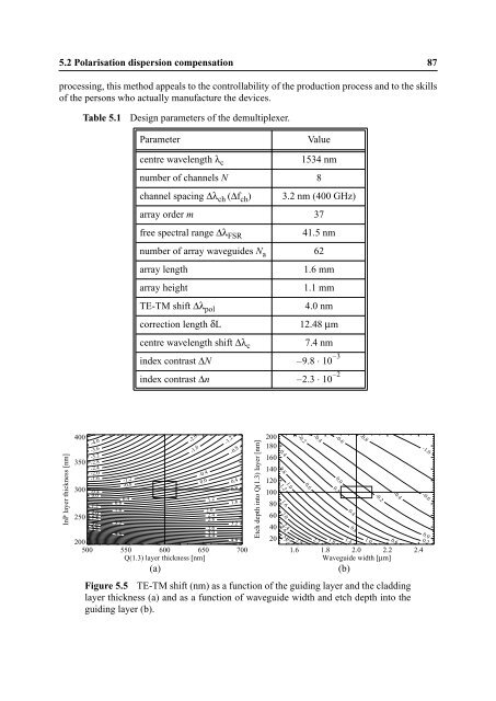
Table 5.1 Design parameters of the demultiplexer.<br />
-4.0<br />
-3.6<br />
-3.2<br />
-2.8<br />
-2.4<br />
-2.0<br />
-1.6<br />
-0.4<br />
0.0<br />
1.2<br />
2.0<br />
2.4<br />
2.8<br />
3.6<br />
4.0<br />
4.4<br />
0.8<br />
1.6<br />
3.2<br />
4.8<br />
-1.2<br />
-0.8<br />
0.4<br />
Parameter Value<br />
centre <strong>wavelength</strong> λ c<br />
1534 nm<br />
number of channels N 8<br />
channel spacing Δλ ch (Δf ch ) 3.2 nm (400 GHz)<br />
array order m 37<br />
free spectral range Δλ FSR<br />
number of array waveguides N a<br />
41.5 nm<br />
62<br />
array length 1.6 mm<br />
array height 1.1 mm<br />
TE-TM shift Δλ pol<br />
4.0 nm<br />
correction length δL 12.48 μm<br />
centre <strong>wavelength</strong> shift Δλ c<br />
index contrast ΔN<br />
index contrast Δn<br />
200<br />
500 550 600 650 700<br />
Q(1.3) layer thickness [nm]<br />
-2.0<br />
-1.6<br />
-0.4<br />
0.0<br />
1.2<br />
2.0<br />
2.4<br />
2.8<br />
3.6<br />
4.0<br />
4.4<br />
-1.2<br />
-0.8<br />
0.4<br />
0.8<br />
1.6<br />
3.2<br />
4.8<br />
Etch depth into Q(1.3) layer [nm]<br />
200<br />
180<br />
160<br />
140<br />
120<br />
100<br />
7.4 nm<br />
– 9.8 10 3 –<br />
⋅<br />
– 2.3 10 2 –<br />
⋅<br />
(a) (b)<br />
80<br />
60<br />
40<br />
20<br />
1.2<br />
1.6<br />
2.0<br />
2.4<br />
3.0<br />
3.2<br />
2.8<br />
2.2<br />
1.8<br />
1.4<br />
1.6 1.8 2.0 2.2 2.4<br />
Waveguide width [μm]<br />
Figure 5.5 TE-TM shift (nm) as a function of the guiding layer and the cladding<br />
layer thickness (a) and as a function of waveguide width and etch depth into the<br />
guiding layer (b).<br />
0.4<br />
0.8<br />
2.6<br />
1.0<br />
-0.2<br />
0.6<br />
-0.4<br />
0.2<br />
-0.6<br />
0.0<br />
0.4<br />
0.8<br />
-0.8<br />
1.0<br />
-0.2<br />
-0.4<br />
0.6<br />
-1.0<br />
-0.6<br />
0.0<br />
0.2