Smart Highside Power Switch - Farnell
Smart Highside Power Switch - Farnell
Smart Highside Power Switch - Farnell

You also want an ePaper? Increase the reach of your titles
YUMPU automatically turns print PDFs into web optimized ePapers that Google loves.
<strong>Smart</strong> <strong>Highside</strong> <strong>Power</strong> <strong>Switch</strong><br />
Reversave<br />
• Reverse battery protection by self turn on of<br />
power MOSFET<br />
Inversave<br />
• Inverse operation by self turn on of power<br />
MOSFET<br />
PROFET® BTS 6133D<br />
Features<br />
Package<br />
• Short circuit protection with latch<br />
PG-TO252-5-11<br />
• Current limitation<br />
(DPAK 5 pin; less than half the size as TO 220 SMD)<br />
• Overload protection<br />
• Thermal shutdown with restart<br />
• Overvoltage protection (including load dump)<br />
• Loss of ground protection<br />
• Loss of Vbb protection (with external diode for<br />
charged inductive loads)<br />
• Very low standby current<br />
• Fast demagnetisation of inductive loads<br />
• Electrostatic discharge (ESD) protection<br />
• Optimized static electromagnetic compatibility (EMC)<br />
• Green Product (RoHS compliant)<br />
• AEC qualified<br />
Diagnostic Function<br />
• Proportional load current sense (with defined fault signal in case of overload operation, overtemperature<br />
shutdown and/or short circuit shutdown)<br />
Application<br />
• <strong>Power</strong> switch with current sense diagnostic feedback for 12V and 24 V DC grounded loads<br />
• All types of resistive, inductive and capacitive loads<br />
• Replaces electromechanical relays, fuses and discrete circuits<br />
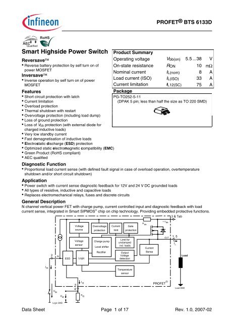
General Description<br />
N channel vertical power FET with charge pump, current controlled input and diagnostic feedback with load<br />
current sense, integrated in <strong>Smart</strong> SIPMOS ® chip on chip technology. Providing embedded protective functions.<br />
I IN<br />
2<br />
V IN<br />
IN<br />
V IS<br />
Logic GND<br />
ESD<br />
Voltage<br />
source<br />
Voltage<br />
sensor<br />
IS<br />
4<br />
Logic<br />
I IS<br />
R IS<br />
Overvoltage<br />
protection<br />
Charge pump<br />
Level shifter<br />
Rectifier<br />
Product Summary<br />
Operating voltage Vbb(on) 5.5 ... 38 V<br />
On-state resistance RON 10 mΩ<br />
Nominal current IL(nom) 8 A<br />
Load current (ISO) IL(ISO) 33 A<br />
Current limitation IL12(SC) 75 A<br />
Current<br />
limit<br />
Gate<br />
protection<br />
Limit for<br />
unclamped<br />
ind. loads<br />
Output<br />
Voltage<br />
detection<br />
Temperature<br />
sensor<br />
Data Sheet Page 1 of 17 Rev. 1.0, 2007-02<br />
R bb<br />
Current<br />
Sense<br />
+ V bb<br />
OUT<br />
PROFET ®<br />
3 & Tab<br />
1, 5<br />
I L<br />
Load<br />
Load GND
Pin Symbol Function<br />
PROFET® BTS 6133D<br />
1 OUT O Output; output to the load; pin 1 and 5 must be externally<br />
shorted* .<br />
2 IN I Input; activates the power switch if shorted to ground.<br />
Tab/(3) Vbb + Supply Voltage; positive power supply voltage; tab and pin3<br />
are internally shorted.<br />
4 IS S Sense Output; Diagnostic feedback; provides at normal<br />
operation a sense current proportional to the load current; in<br />
case of overload, overtemperature and/or short circuit a<br />
defined current is provided (see Truth Table on page 8)<br />
5 OUT O Output; output to the load; pin 1 and 5 must be externally<br />
shorted*.<br />
*) Not shorting all outputs will considerably increase the on-state resistance, reduce the peak current capability<br />
and decrease the current sense accuracy<br />
Maximum Ratings at Tj = 25 °C unless otherwise specified<br />
Parameter Symbol Values Unit<br />
Supply voltage (overvoltage protection see page 4) Vbb 38 V<br />
Supply voltage for full short circuit protection 1) Vbb 30 V<br />
Load dump protection VLoadDump = UA + Vs, UA = 13.5 V<br />
RI= 2 Ω, RL= 1.5 Ω, td= 400 ms, IN= low or high<br />
VLoad dump 2) 45 V<br />
Load current (Short-circuit current, see page 5) IL self-limited A<br />
Operating temperature range<br />
Tj<br />
-40 ...+150 °C<br />
Storage temperature range<br />
Tstg<br />
-55 ...+150<br />
<strong>Power</strong> dissipation (DC) Ptot 59 W<br />
Inductive load switch-off energy dissipation 3)<br />
single pulse IL = 20 A, Vbb= 12V Tj=150 °C:<br />
Electrostatic discharge capability (ESD)<br />
(Human Body Model)<br />
acc. ESD assn. std. S5.1-1993; R=1.5kΩ; C=100pF<br />
Current through input pin (DC)<br />
Current through current sense pin (DC)<br />
see internal circuit diagrams page 9<br />
Input voltage slew rate<br />
Vbb ≤ 16V :<br />
Vbb > 16V 4) :<br />
EAS 0.3 J<br />
3.0 kV<br />
VESD<br />
Data Sheet Page 2 of 17 Rev. 1.0, 2007-02<br />
IIN<br />
IIS<br />
+15, -120<br />
+15, -120<br />
mA<br />
dVbIN / dt self-limited<br />
20 V/µs<br />
1) Short circuit is defined as a combination of remaining resistances and inductances. See schematic on page<br />
11.<br />
2) VLoad dump is setup without the DUT connected to the generator per ISO 7637-1 and DIN 40839.<br />
3) See also diagram on page 11.<br />
4) See also on page 8. Slew rate limitation can be achieved by means of using a series resistor RIN in the input<br />
path. This resistor is also required for reverse operation. See also page 10.
Thermal Characteristics<br />
PROFET® BTS 6133D<br />
Parameter and Conditions Symbol Values Unit<br />
min typ max<br />
Thermal resistance chip - case: RthJC -- -- 1.1 K/W<br />
junction - ambient (free air): RthJA -- 80 --<br />
SMD version, device on PCB 5) : -- 45 55<br />
Electrical Characteristics<br />
Parameter and Conditions Symbol Values Unit<br />
at Tj= 25, Vbb = 12 V unless otherwise specified min typ max<br />
Load <strong>Switch</strong>ing Capabilities and Characteristics<br />
On-state resistance (pin 3 to pin 1,5)<br />
VIN= 0, Vbb= 5.5V, IL = 7.5 A Tj=25 °C:<br />
Tj=150 °C:<br />
VIN= 0, Vbb= 12V, IL = 7.5 A Tj=25 °C:<br />
Tj=150 °C:<br />
Nominal load current (Tab to pin 1,5)<br />
ISO Proposal: VON ≤ 0.5 V, TC = 85°C, Tj ≤ 150°C<br />
SMD 5) : VON ≤ 0.5 V, TA = 85°C, Tj ≤ 150°C<br />
Turn-on time to 90% VOUT:<br />
Turn-off time to 10% VOUT:<br />
RL = 2.2 Ω, Tj=-40...150 °C<br />
Slew rate on<br />
25 to 50% VOUT, RL = 2.2 Ω, Tj=-40...150 °C<br />
Slew rate off<br />
50 to 25% VOUT, RL = 2.2 Ω, Tj=-40...150 °C<br />
Data Sheet Page 3 of 17 Rev. 1.0, 2007-02<br />
RON<br />
IL(ISO)<br />
IL(nom)<br />
ton<br />
toff<br />
--<br />
--<br />
--<br />
--<br />
33<br />
8<br />
--<br />
--<br />
10<br />
18<br />
8<br />
14<br />
41<br />
10<br />
250<br />
250<br />
14<br />
26<br />
10<br />
18<br />
--<br />
--<br />
500<br />
500<br />
mΩ<br />
A<br />
µs<br />
dV /dton -- 0.3 0.5 V/µs<br />
-dV/dtoff -- 0.3 0.6 V/µs<br />
5) Device on 50mm*50mm*1.5mm epoxy PCB FR4 with 6cm 2 (one layer, 70µm thick) copper area for Vbb<br />
connection. PCB is vertical without blown air.
PROFET® BTS 6133D<br />
Parameter and Conditions Symbol Values Unit<br />
at Tj= 25, Vbb = 12 V unless otherwise specified min typ max<br />
Operating Parameters<br />
Operating voltage (VIN=0) Tj=-40...150 °C: Vbb(on) 5.5 -- 38 V<br />
Undervoltage shutdown 6) 7) VbIN(u) -- 2.5 3.5 V<br />
Undervoltage restart of charge pump Vbb(ucp) -- 4 5.5 V<br />
Overvoltage protection 8)<br />
Ibb=15 mA Tj=-40...+150°C :<br />
VZ,IN<br />
63 67 --<br />
V<br />
Standby current Tj=-40...+120°C:<br />
IIN=0 Tj=150°C:<br />
Reverse Battery<br />
Ibb(off)<br />
Reverse battery voltage 9) -Vbb -- -- 16 V<br />
On-state resistance (pin 1,5 to pin 3)<br />
Vbb= - 8V, VIN= 0, IL = -7.5 A, RIS = 1 kΩ, 7)<br />
Tj=25 °C:<br />
Tj=150 °C:<br />
Vbb= -12V, VIN= 0, IL = -7.5 A, RIS = 1 kΩ, Tj=25 °C:<br />
Tj=150 °C:<br />
RON(rev)<br />
Integrated resistor in Vbb line Rbb -- 100 150 Ω<br />
Inverse Load Current Operation<br />
On-state resistance (Pins 1,5 to pin 3) 7)<br />
VbIN = 12 V, IL = - 7.5 A Tj = 25 °C:<br />
See diagram on page 10 Tj = 150 °C:<br />
7) 10)<br />
Maximum transient inverse load current<br />
(Pins 1,5 to Tab)<br />
Tj = 25 °C<br />
Tj = 85 °C<br />
Tj = 150 °C<br />
Drain-source diode voltage (+Vout<br />
IL = - 7.5 A, IIN = 0, Tj = 150°C<br />
> +Vbb) 7)<br />
RON(inv)<br />
- IL(inv)<br />
Data Sheet Page 4 of 17 Rev. 1.0, 2007-02<br />
--<br />
--<br />
--<br />
--<br />
--<br />
--<br />
--<br />
--<br />
--<br />
--<br />
--<br />
3<br />
6<br />
9.5<br />
16<br />
9<br />
15<br />
8<br />
14<br />
--<br />
--<br />
--<br />
6<br />
14<br />
13<br />
22<br />
12<br />
21<br />
10<br />
18<br />
45<br />
30<br />
14<br />
µA<br />
mΩ<br />
mΩ<br />
-VON -- 0.3 -- V<br />
6) VbIN=Vbb-VIN see schematic on page 8 and on page 14.<br />
7) Not subject to production test, specified by design.<br />
8) See also VZ,IN in schematic on page 9.<br />
9) For operation at voltages higher then |16V| please see required schematic on page 10.<br />
10) Operation above these limits might cause a switch off of the device after the transition from inverse to<br />
forward mode. In this case the device switches on again after a time delay of typ.1 msec.<br />
A
PROFET® BTS 6133D<br />
Parameter and Conditions Symbol Values Unit<br />
at Tj= 25, Vbb = 12 V unless otherwise specified min typ max<br />
Protection Functions 11)<br />
Short circuit current limit (Tab to pin 1,5) 12)<br />
Short circuit current limit at VON = 6V 13) Tj =-40°C:<br />
Tj =25°C:<br />
Tj =+150°C:<br />
Short circuit current limit at VON = 12V Tj(start) =-40°C:<br />
tm=170µs Tj(start) =25°C:<br />
Tj(start) =+150°C:<br />
Short circuit current limit at VON = 18V 13) Tj(start) =-40°C:<br />
Tj(start) =25°C:<br />
Tj(start) =+150°C:<br />
Short circuit current limit at VON = 24V Tj(start) =-40°C:<br />
tm=170µs Tj(start) =25°C:<br />
Tj(start) =+150°C:<br />
Short circuit current limit at VON = 30V 13) Tj(start) =-40°C:<br />
Tj(start) =25°C:<br />
Tj(start) =+150°C:<br />
Short circuit shutdown detection voltage<br />
(pin 3 to pins 1,5)<br />
IL6(SC)<br />
IL12(SC)<br />
IL18(SC)<br />
IL24(SC)<br />
IL30(SC)<br />
VON(SC)<br />
Data Sheet Page 5 of 17 Rev. 1.0, 2007-02<br />
--<br />
--<br />
70<br />
--<br />
--<br />
45<br />
--<br />
--<br />
33<br />
--<br />
--<br />
20<br />
--<br />
--<br />
15<br />
2.5<br />
110<br />
105<br />
90<br />
80<br />
75<br />
60<br />
60<br />
55<br />
50<br />
40<br />
40<br />
35<br />
25<br />
25<br />
25<br />
140<br />
--<br />
--<br />
110<br />
--<br />
--<br />
80<br />
--<br />
--<br />
60<br />
--<br />
--<br />
40<br />
--<br />
--<br />
A<br />
A<br />
A<br />
A<br />
A<br />
3.5 4.5 V<br />
Short circuit shutdown delay after input current<br />
positive slope, VON > VON(SC), Tj = -40...+150°C<br />
min. value valid only if input "off-signal" time exceeds 30 µs<br />
Short circuit shutdown delay during on condition<br />
td(SC1) 350 650 1200 µs<br />
13)<br />
VON > VON(SC)<br />
td(SC2) -- 2 -- µs<br />
Output clamp (inductive load switch off) 14)<br />
at VOUT = Vbb - VON(CL) (e.g. overvoltage)<br />
IL= 40 mA<br />
VON(CL) 39 42 -- V<br />
Thermal overload trip temperature Tjt 150 175 -- °C<br />
Thermal hysteresis ∆Tjt -- 10 -- K<br />
11) Integrated protection functions are designed to prevent IC destruction under fault conditions described in the<br />
data sheet. Fault conditions are considered as "outside" normal operating range. Protection functions are not<br />
designed for continuous repetitive operation.<br />
12) Short circuit current limit for max. duration of td(SC1) , prior to shutdown, see also figures 3.x on page 13.<br />
13) Not subject to production test, specified by design.<br />
14) See also figure 2b on page 12.
PROFET® BTS 6133D<br />
Parameter and Conditions Symbol Values Unit<br />
at Tj= 25, Vbb = 12 V unless otherwise specified min typ max<br />
Diagnostic Characteristics<br />
Current sense ratio, static on-condition<br />
kILIS = IL : IIS, IIS < IIS,lim 15) ,<br />
VIS 4.5 V<br />
IL = 30A, Tj = -40°C:<br />
Tj = +25°C:<br />
Tj = +150°C:<br />
IL = 7.5A, Tj = -40°C:<br />
Tj = +25°C:<br />
Tj = +150°C:<br />
IL = 2.5A, Tj = -40°C:<br />
Tj = +25°C:<br />
Tj = +150°C:<br />
Data Sheet Page 6 of 17 Rev. 1.0, 2007-02<br />
KILIS<br />
--<br />
8300<br />
8300<br />
8300<br />
7500<br />
8000<br />
8200<br />
6100<br />
6500<br />
7600<br />
10 000 --<br />
10000<br />
9700<br />
9300<br />
10000<br />
9700<br />
9300<br />
10000<br />
9700<br />
9300<br />
11000<br />
10600<br />
10000<br />
11400<br />
10800<br />
10200<br />
14200<br />
12800<br />
11500<br />
IIN = 0 (e.g. during deenergizing of inductive loads): -- 0 --<br />
Sense current under fault conditions 16)<br />
V ON >1V, typ Tj = -40...+150°C:<br />
Sense saturation current<br />
V ON 1V, Tj = -40...+150°C<br />
IIS,fault<br />
IIS,lim<br />
4.0<br />
4.0<br />
5.2 7.5 mA<br />
6.0 7.5 mA<br />
tdelay(fault) 350 650 1200 µs<br />
Current sense leakage current, IIN = 0 IIS(LL) -- 0.1 0.5 µA<br />
Current sense offset current, VIN = 0, IL ≤ 0 IIS(LH) -- 1 60 µA<br />
Current sense settling time to IIS static after input<br />
current positive slope, 17)<br />
IL = 0 20 A, Tj= -40...+150°C<br />
Current sense settling time during on condition, 17)<br />
IL = 10 20 A, Tj= -40...+150°C<br />
Overvoltage protection<br />
Ibb = 15 mA Tj = -40...+150°C:<br />
tson(IS)<br />
tslc(IS)<br />
VZ,IS<br />
--<br />
--<br />
63<br />
250 500 µs<br />
50 100 µs<br />
67 -- V<br />
15) See also figures 4.x and 6.x on page 13 and 14.<br />
16) Fault conditions are overload during on (i.e. VON>1V typ.), overtemperature and short circuit; see also truth<br />
table on page 8.<br />
17) Not subject to production test, specified by design.
PROFET® BTS 6133D<br />
Parameter and Conditions Symbol Values Unit<br />
at Tj= 25, Vbb = 12 V unless otherwise specified min typ max<br />
Input<br />
Required current capability of input switch IIN(on)<br />
Tj =-40..+150°C:<br />
-- 1.4 2.2 mA<br />
Input current for turn-off Tj =-40..+150°C: IIN(off) -- -- 30 µA<br />
Data Sheet Page 7 of 17 Rev. 1.0, 2007-02
Truth Table<br />
Input<br />
Current<br />
level<br />
Normal<br />
L<br />
operation<br />
H<br />
Overload 18) L<br />
H<br />
Short circuit to GND 19) L<br />
H<br />
Overtemperature L<br />
H<br />
Short circuit to Vbb L<br />
H<br />
Open load L<br />
H<br />
Output<br />
level<br />
L<br />
H<br />
L<br />
H<br />
L<br />
L<br />
L<br />
L<br />
H<br />
H<br />
Current<br />
Sense<br />
IIS<br />
≈0 (IIS(LL))<br />
nominal<br />
≈0 (IIS(LL))<br />
IIS,fault ≈0 (IIS(LL))<br />
IIS,fault ≈0 (IIS(LL))<br />
IIS,fault ≈0 (IIS(LL))<br />
3.5V (typ.) . See also page 11.<br />
20) Low ohmic short to Vbb may reduce the output current IL and therefore also the sense current IIS.<br />
Data Sheet Page 8 of 17 Rev. 1.0, 2007-02<br />
Z<br />
H
Input circuit (ESD protection)<br />
V bIN<br />
V Z,IN<br />
IN<br />
V IN<br />
I<br />
IN<br />
ZD<br />
ESD-Zener diode: 67 V typ., max 15 mA;<br />
Current sense output<br />
Normal operation<br />
V bb<br />
R bb<br />
I IS,fault<br />
ZD<br />
I IS<br />
V<br />
Z,IS<br />
IS<br />
R<br />
IS<br />
R bb<br />
V<br />
IS<br />
V bb<br />
VZ,IS = 67 V (typ.), RIS = 1 kΩ nominal (or 1 kΩ /n, if n<br />
devices are connected in parallel). IS = IL/kilis can be<br />
only driven by the internal circuit as long as<br />
Vout - VIS > 5V. Therefore RIS should be less than<br />
Vbb − 5V<br />
7.<br />
5mA<br />
Note: For large values of RIS the voltage VIS can reach<br />
almost Vbb. See also overvoltage protection.<br />
If you don't use the current sense output in your<br />
application, you can leave it open.<br />
.<br />
PROFET® BTS 6133D<br />
Inductive and overvoltage output clamp<br />
Data Sheet Page 9 of 17 Rev. 1.0, 2007-02<br />
V Z1<br />
PROFET<br />
VON is clamped to VON(Cl) = 42 V typ<br />
+ V bb<br />
V ON<br />
OUT<br />
Overvoltage protection of logic part<br />
R IN<br />
IN<br />
V Z,IN<br />
R IS<br />
IS<br />
V Z,IS<br />
Logic<br />
R V<br />
Signal GND<br />
R bb<br />
PROFET<br />
V Z,VIS<br />
+ V bb<br />
V OUT<br />
Rbb = 100 Ω typ., VZ,IN = VZ,IS = 67 V typ., RIS = 1 kΩ<br />
nominal. Note that when overvoltage exceeds 67 V typ.<br />
a voltage above 5V can occur between IS and GND, if<br />
RV, VZ,VIS are not used.
Reversave (Reverse battery protection)<br />
R<br />
IN<br />
IN<br />
D<br />
Logic<br />
Signal GND<br />
R<br />
IS<br />
R<br />
bb<br />
<strong>Power</strong><br />
Transistor<br />
R<br />
L<br />
<strong>Power</strong> GND<br />
-Vbb<br />
OUT<br />
RIS typ. 1 kΩ. Add RIN for reverse battery protection in<br />
applications with Vbb above 16V;<br />
1<br />
R<br />
recommended value: + =<br />
IN<br />
1<br />
R<br />
IS<br />
0.<br />
08A<br />
| V | −12V<br />
To minimise power dissipation at reverse battery<br />
operation, the overall current into the IN and IS pin<br />
should be about 80mA. The current can be provided by<br />
using a small signal diode D in parallel to the input<br />
switch, by using a MOSFET input switch or by proper<br />
adjusting the current through RIS.<br />
Since the current via Rbb generates additional heat in<br />
the device, this has to be taken into account in the<br />
overall thermal consideration.<br />
Inversave (Inverse current operation)<br />
+<br />
V bb<br />
V<br />
bb<br />
bb<br />
IN PROFET OUT<br />
- IL<br />
IS<br />
-<br />
V<br />
OUT +<br />
V IN<br />
V IS<br />
R IS<br />
The device can be operated in inverse load current<br />
mode (VOUT > Vbb > 0V). The current sense feature is<br />
not available during this kind of operation (IIS= IIS(LH)).<br />
With IIN = 0 (e.g. input open) only the intrinsic drain<br />
source diode is conducting resulting in considerably<br />
increased power dissipation. If the device is switched<br />
on (VIN = 0), the power dissipation is decreased to the<br />
much lower value RON(INV) * I 2 as long as a maximum<br />
current IL(inv) is not exceeded(see on p4).<br />
Note: Temperature protection during inverse load<br />
current operation is not possible!<br />
I IS<br />
-<br />
PROFET® BTS 6133D<br />
Vbb disconnect with energised inductive<br />
load<br />
Provide a current path with load current capability by<br />
using a diode, a Z-diode, or a varistor. (VZL+VD
Short circuit detection<br />
Fault Condition: V ON > VON(SC) (3.5 V typ.) and t> td(SC)<br />
(typ.650 µs).<br />
Overload detection<br />
Fault Condition: V ON > 1 V typ.<br />
Logic<br />
unit<br />
Short circuit<br />
detection<br />
circuit<br />
Short circuit is a combination of primary and<br />
secondary impedance’s and a resistance’s.<br />
5uH<br />
10mOhm<br />
V bb<br />
I IN<br />
IN<br />
V<br />
bb<br />
PROFET<br />
IS<br />
SC<br />
OUT<br />
+ V bb<br />
V ON<br />
OUT<br />
L SC<br />
R SC<br />
Allowable combinations of minimum, secondary<br />
resistance for full protection at given secondary<br />
inductance and supply voltage for single short circuit<br />
event:<br />
L<br />
[uH] SC<br />
V : 16V<br />
15 bb 18V 24V 30V<br />
10<br />
5<br />
0<br />
0 100 200<br />
300<br />
Z L<br />
R SC<br />
[mOhm]<br />
PROFET® BTS 6133D<br />
Inductive load switch-off energy<br />
dissipation<br />
PROFET<br />
Data Sheet Page 11 of 17 Rev. 1.0, 2007-02<br />
V bb<br />
E bb<br />
I IN<br />
IN<br />
V<br />
bb<br />
IS<br />
R IS<br />
OUT<br />
E AS<br />
{<br />
Z L<br />
i (t)<br />
L<br />
Energy stored in load inductance:<br />
EL = 1 /2·L·I 2<br />
L<br />
While demagnetising load inductance, the energy<br />
dissipated in PROFET is<br />
EAS= Ebb + EL - ER= ∫ VON(CL) ·iL (t) dt,<br />
with an approximate solution for R L > 0 Ω:<br />
EAS=<br />
L<br />
R L<br />
E Load<br />
E<br />
L<br />
E R<br />
IL· L<br />
IL·RL<br />
(V<br />
2·R bb + |VOUT(CL)|) ln (1+<br />
L<br />
|VOUT(CL)| )<br />
Maximum allowable load inductance for<br />
a single switch off<br />
L = f (I L ); T j,start = 150°C, V bb = 12 V, R L = 0 Ω<br />
1000<br />
L [mH]<br />
100<br />
10<br />
1<br />
0,1<br />
0,01<br />
1 10 I_L [A] 100
Timing diagrams<br />
Figure 1a: <strong>Switch</strong>ing a resistive load,<br />
change of load current in on-condition:<br />
I IN<br />
V OUT<br />
90%<br />
10%<br />
I L<br />
I IS<br />
t on<br />
dV/dton<br />
t t<br />
slc(IS)<br />
Load 1 Load 2<br />
t son(IS)<br />
tsoff(IS)<br />
t off<br />
slc(IS)<br />
dV/dtoff<br />
The sense signal is not valid during a settling time<br />
after turn-on/off and after change of load current.<br />
t<br />
PROFET® BTS 6133D<br />
Figure 2a: <strong>Switch</strong>ing motors and lamps:<br />
Data Sheet Page 12 of 17 Rev. 1.0, 2007-02<br />
I IN<br />
V OUT<br />
I IL<br />
I IS I IS,faut / I IS,lim<br />
As long as V bIS < V Z,IS the sense current will never<br />
exceed I IS,fault and/or I IS,lim .<br />
Figure 2b: <strong>Switch</strong>ing an inductive load:<br />
I IN<br />
V OUT<br />
I L<br />
I IS<br />
V ON(CL)<br />
t<br />
t
Figure 3a: Typ. current limitation characteristic<br />
[A] I L(SC)<br />
100<br />
80<br />
60<br />
40<br />
20<br />
0<br />
0 10 20<br />
V ON(SC)<br />
30<br />
[V]<br />
V ON<br />
In case of VON > VON(SC) (typ. 3.5 V) the device will<br />
be switched off by internal short circuit detection.<br />
Figure 3b: Short circuit type one:<br />
shut down by short circuit detection, reset by IIN = 0.<br />
I L<br />
I IN<br />
IIS<br />
tm<br />
VON > VON(SC)<br />
IL(SC)<br />
td(SC1)<br />
I IS,fault<br />
tdelay(fault)<br />
Shut down remains latched until next reset via input.<br />
t<br />
PROFET® BTS 6133D<br />
Figure 3c: Short circuit type two:<br />
shut down by short circuit detection, reset by IIN = 0.<br />
Data Sheet Page 13 of 17 Rev. 1.0, 2007-02<br />
I L<br />
I IN<br />
V ON<br />
IIS<br />
td(SC2)<br />
1V typ.<br />
IL k ilis<br />
Internal <strong>Switch</strong> off<br />
depending on the<br />
external impedance<br />
I IS,fault<br />
Shut down remains latched until next reset via input.<br />
Figure 4a: Overtemperature<br />
Reset if Tj
Figure 4b: Overload<br />
Tj
Package Outlines<br />
All dimensions in mm<br />
D-Pak-5 Pin: PG-TO252-5-11<br />
Sales Code BTS 6133D<br />
PROFET® BTS 6133D<br />
Green Product<br />
To meet the world-wide customer requirements for environmentally friendly products and to be compliant with<br />
government regulations the device is available as a green product. Green products are RoHS-Compliant (i.e Pbfree<br />
finish on leads and suitable for Pb-free soldering according to IPC/JEDEC J-STD-020).<br />
Data Sheet Page 15 of 17 Rev. 1.0, 2007-02
Revision History<br />
PROFET® BTS 6133D<br />
Version Date Changes<br />
Rev. 1.0 2007-02-21 RoHS-compliant version of BTS6133D<br />
Page 1, page 16: RoHS compliance statement and Green product feature added<br />
Page 1, page 16: Change to RoHS compliant package PG-TO252-5-11<br />
Legal disclaimer updated<br />
Data Sheet Page 16 of 17 Rev. 1.0, 2007-02
Edition 2007-02<br />
Published by<br />
Infineon Technologies AG<br />
81726 Munich, Germany<br />
© Infineon Technologies AG 2007.<br />
All Rights Reserved.<br />
Legal Disclaimer<br />
The information given in this document shall in no event be regarded as a guarantee of conditions or<br />
characteristics (“Beschaffenheitsgarantie”). With respect to any examples or hints given herein, any typical<br />
values stated herein and/or any information regarding the application of the device, Infineon Technologies<br />
hereby disclaims any and all warranties and liabilities of any kind, including without limitation warranties of noninfringement<br />
of intellectual property rights of any third party.<br />
Information<br />
For further information on technology, delivery terms and conditions and prices please contact your nearest<br />
Infineon Technologies Office (www.infineon.com).<br />
Warnings<br />
Due to technical requirements components may contain dangerous substances. For information on the types in<br />
question please contact your nearest Infineon Technologies Office.<br />
Infineon Technologies Components may only be used in life-support devices or systems with the express written<br />
approval of Infineon Technologies, if a failure of such components can reasonably be expected to cause the<br />
failure of that life-support device or system, or to affect the safety or effectiveness of that device or system. Life<br />
support devices or systems are intended to be implanted in the human body, or to support and/or maintain and<br />
sustain and/or protect human life. If they fail, it is reasonable to assume that the health of the user or other<br />
persons may be endangered.