here. - Power Electronics
here. - Power Electronics
here. - Power Electronics
You also want an ePaper? Increase the reach of your titles
YUMPU automatically turns print PDFs into web optimized ePapers that Google loves.
Tackling the Challenges<br />
of <strong>Power</strong> Dissipation<br />
Simple thermal calculations and bench tests<br />
enable small outline devices such as the DFN<br />
to deliver high currents.<br />
Integrated circuit manufacturers are working furiously<br />
to reduce the package sizes of power devices<br />
for their customer base. This effort has been<br />
well received, particularly w<strong>here</strong> portable applications<br />
are involved. Some of the newer packages in<br />
which these power devices are being housed include the<br />
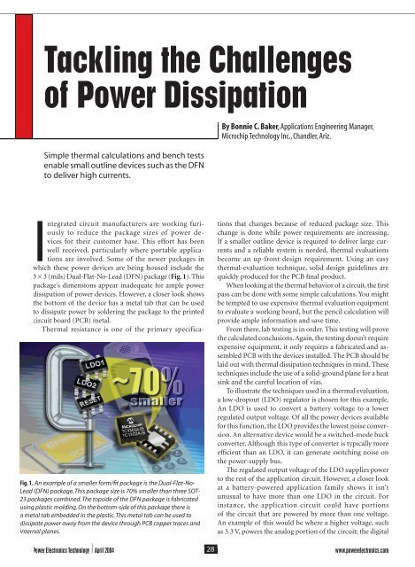
3 × 3 (mils) Dual-Flat-No-Lead (DFN) package (Fig. 1). This<br />
package’s dimensions appear inadequate for ample power<br />
dissipation of power devices. However, a closer look shows<br />
the bottom of the device has a metal tab that can be used<br />
to dissipate power by soldering the package to the printed<br />
circuit board (PCB) metal.<br />
Thermal resistance is one of the primary specifica-<br />
Fig. 1. An example of a smaller form/fi t package is the Dual-Flat-No-<br />
Lead (DFN) package. This package size is 70% smaller than three SOT-<br />
23 packages combined. The topside of the DFN package is fabricated<br />
using plastic molding. On the bottom-side of this package t<strong>here</strong> is<br />
a metal tab embedded in the plastic. This metal tab can be used to<br />
dissipate power away from the device through PCB copper traces and<br />
internal planes.<br />
By Bonnie C. Baker, Baker Applications Engineering Manager,<br />
Microchip Technology Inc., Chandler, Ariz.<br />
tions that changes because of reduced package size. This<br />
change is done while power requirements are increasing.<br />
If a smaller outline device is required to deliver large currents<br />
and a reliable system is needed, thermal evaluations<br />
become an up-front design requirement. Using an easy<br />
thermal-evaluation technique, solid design guidelines are<br />
quickly produced for the PCB fi nal product.<br />
When looking at the thermal behavior of a circuit, the fi rst<br />
pass can be done with some simple calculations. You might<br />
be tempted to use expensive thermal evaluation equipment<br />
to evaluate a working board, but the pencil calculation will<br />
provide ample information and save time.<br />
From t<strong>here</strong>, lab testing is in order. This testing will prove<br />
the calculated conclusions. Again, the testing doesn’t require<br />
expensive equipment, it only requires a fabricated and assembled<br />
PCB with the devices installed. The PCB should be<br />
laid out with thermal dissipation techniques in mind. These<br />
techniques include the use of a solid-ground plane for a heat<br />
sink and the careful location of vias.<br />
To illustrate the techniques used in a thermal evaluation,<br />
a low-dropout (LDO) regulator is chosen for this example.<br />
An LDO is used to convert a battery voltage to a lower<br />
regulated output voltage. Of all the power devices available<br />
for this function, the LDO provides the lowest noise conversion.<br />
An alternative device would be a switched-mode buck<br />
converter. Although this type of converter is typically more<br />
effi cient than an LDO, it can generate switching noise on<br />
the power-supply bus.<br />
The regulated output voltage of the LDO supplies power<br />
to the rest of the application circuit. However, a closer look<br />
at a battery-powered application family shows it isn’t<br />
unusual to have more than one LDO in the circuit. For<br />
instance, the application circuit could have portions<br />
of the circuit that are powered by more than one voltage.<br />
An example of this would be w<strong>here</strong> a higher voltage, such<br />
as 3.3 V, powers the analog portion of the circuit; the digital<br />
<strong>Power</strong> <strong>Electronics</strong> Technology April 2004 28<br />
www.powerelectronics.com
POWER DISSIPATION<br />
<br />
<br />
<br />
<br />
<br />
<br />
<br />
<br />
Fig. 2. In this DFN package, the internal junction temperature (T ) indi-<br />
J<br />
cates the temperature of the silicon chip, and the case temperature (T ) C ) C<br />
describes the temperature on the case of the device. This temperature<br />
is measured on the exposed metal pad that spans across the bottomside<br />
of the package. This metal pad is soldered to the board<br />
to remove heat from the package. The ambient temperature (T ) quan-<br />
A<br />
tifi es the temperature of the surrounding atmosp<strong>here</strong>. [1]<br />
portion of the circuit is powered with a 1.8-V power-supply<br />
voltage. Another application type is w<strong>here</strong> several portions of<br />
the circuit require some degree of isolation but also require<br />
the same voltage. In this type of system, some portions of<br />
the circuit can be turned off, while others are left on. In yet<br />
another application, power sequencing of various portions<br />
of the circuit is required.<br />
These kinds of applications could prompt a designer<br />
to use a dual LDO instead of a single LDO. The dual LDO<br />
conserves board space and typically improves overall price.<br />
Both features are attractive, but the dual LDO dissipates the<br />
power of both LDOs in one package. The smaller package,<br />
whether it contains a dual or a single LDO, may have a higher<br />
thermal resistance.<br />
To summarize, this dual LDO device dissipates more<br />
power (or heat) and is housed in a less-effi cient thermal<br />
package. These conditions are aggressive, but the challenge<br />
of dissipating the heat can be worked out as follows.<br />
An example of a dual LDO is the TC1301B from<br />
Microchip Technology Inc. One of the smaller geometry<br />
packages that house this dual LDO is the 3 × 3 (mil) DFN.<br />
Figs. 1 and 2 show a diagram of the DFN package.<br />
This device combines two LDO regulators and a microcontroller<br />
RESET function into a single 8-pin, 3 × 3<br />
mil DFN package. Regulator number one (LDO 1 ) inside<br />
this package has a dropout voltage of 104 mV at 300 mA<br />
output current (typical). Regulator number two (LDO 2 )<br />
has a dropout voltage of 150 mV at 150 mA (typical). [1]<br />
The maximum allowable steady-state junction temperature<br />
of the TC1301B is 125°C. The TC1301B has a convenient<br />
thermal-shutdown feature that facilitates thermal evaluations.<br />
This device goes into a thermal shutdown mode at<br />
150°C (typical).<br />
<strong>Power</strong> <strong>Electronics</strong> Technology April 2004<br />
CIRCLE 232 on Reader Service Card or freeproductinfo.net/pet<br />
30<br />
www.powerelectronics.com
The TC1301B power dissipation is 780 mW, given the<br />
following conditions:<br />
Input voltage = 4.2 V<br />
Output voltage of LDO = 2.8 V @ 300 mA<br />
1<br />
Output voltage of LDO = 1.8 V @ 150 mA<br />
2<br />
The maximum power dissipated by the device can be<br />
calculated by:<br />
P = (V – V )/ I D (MAX) IN (MAX) OUT (MAX) OUT (MAX)<br />
W<strong>here</strong> P is the maximum device power dissipa-<br />
D (MAX)<br />
tion<br />
V is the maximum input voltage to the device.<br />
IN (MAX)<br />
V is the maximum output voltage of the device.<br />
OUT (MAX) (MAX)<br />
I is the maximum output current of the device.<br />
OUT (MAX)<br />
The power dissipation of the device is equal to:<br />
P = (V –V )×I D LDO1 (MAX) IN (MAX) OUT-LDO1 (MAX)<br />
OUT-LDO1 (MAX)<br />
P = (4.2 V–2.8 V)×300 mA<br />
D LDO1 (MAX)<br />
P = 0.42 W<br />
D LDO1 (MAX)<br />
P = (V –V )×I D LDO2 (MAX) IN (MAX) OUT-LDO2 (MAX)<br />
OUT-LDO2 (MAX)<br />
P D LDO2 (MAX) = (4.2V–1.8 V)×150 mA<br />
P D LDO2 (MAX) = 0.36 W<br />
P D TOTAL (MAX) = P D LDO1 (MAX) +P D LDO2 (MAX)<br />
P D TOTAL (MAX) = 0.78 W<br />
The thermal resistance junction-to-ambient (R JA ) of<br />
the DFN package is 41°C/W. This DFN thermal resistance<br />
specifi cation is based on the 4-layer test method described<br />
<br />
<br />
<br />
in the EIA/JEDEC [3] JESD51-5 and JESD51-7 standards. In<br />
the JESD51 specifi cation, some of the conditions that the<br />
test calls out are a 4-layer board, with copper thickness of<br />
2 oz on the outer layers, and 1 oz on the inner layers. They<br />
also specify two vias be connected to the exposed bottom<br />
pad of the DFN package. These vias also are connected to<br />
the ground plane.<br />
www.powerelectronics.com<br />
CIRCLE 234 on Reader Service Card or freeproductinfo.net/pet<br />
33<br />
<strong>Power</strong> <strong>Electronics</strong> Technology April 2004<br />
<br />
POWER DISSIPATION<br />
<br />
<br />
<br />
<br />
<br />
<br />
<br />
<br />
Fig. 3. The chip junction temperature of the DFN package (T ), case tem-<br />
J<br />
perature (T ), and ambient temperature (T ) are used in the package<br />
C A<br />
thermal model, w<strong>here</strong> R is the junction-case thermal resistance and<br />
JC<br />
JC<br />
R is the case-ambient thermal resistance. CA [2]
POWER DISSIPATION<br />
These details are mentioned because<br />
many application boards don’t<br />
have the 4-layers. Additionally, the<br />
copper weight of many boards is 0.5<br />
oz instead of the 1 oz and 2 oz called<br />
out by EIA/JEDEC. These differences<br />
will produce results that are different<br />
as compared to those specified by<br />
EIA/JEDEC. Furthermore, these EIA/<br />
JEDEC conditions are different than<br />
the standard EIA/JEDEC conditions<br />
that are called out for packages other<br />
than the DFN package.<br />
The model in Fig. 3 can be used to<br />
do fi rst-order thermal calculations.<br />
This model is put in the simple terms<br />
of an electrical system, w<strong>here</strong> power<br />
is illustrated as a current source, temperature<br />
is referenced as a voltage<br />
and thermal resistance is illustrated<br />
as a resistance. The defi nitions of the<br />
variables in this model are:<br />
I SOURCE = <strong>Power</strong> in Watts<br />
T J = Chip junction temperature in °C<br />
T = Device case temperature in °C<br />
C<br />
T = Ambient temperature in °C<br />
<br />
<br />
T A<br />
R = Thermal resistance from chip junction to device<br />
JC<br />
case in °C/W<br />
R = Thermal resistance from device case to copper<br />
CS<br />
ground plane (PC board) in °C/W<br />
R = Thermal resistance from device copper-ground<br />
SA<br />
plane to ambient (air) in °C/W<br />
Given the above specifi cations, the rise in temperature at<br />
the junction above ambient of the TC1301B is:<br />
T = P * R J(RISE) TOTAL JA<br />
T = 780 mW * 41°C/W<br />
J(RISE)<br />
T = 32°C<br />
J(RISE)<br />
The thermal resistance from junction to ambient with<br />
a 2-layer board with vias to the copper ground plane that<br />
<br />
<br />
<br />
<br />
<br />
<br />
<br />
<br />
<br />
<br />
<br />
<br />
<br />
<br />
<br />
have been poorly placed can be as high<br />
as 150°C/W. With this type of layout,<br />
the capacitors are connected using vias<br />
to the copper ground plane without<br />
consideration to thermal issues. With<br />
these conditions, the rise in junction<br />
temperature is:<br />
T J(RISE) = P TOTAL * R JA<br />
T J(RISE) = 780 mW * 150°C/W<br />
T J(RISE) = 117°C<br />
If this simple 2-layer layout were<br />
used in an ambient environment of<br />
25°C, the junction temperature would<br />
be equal to:<br />
T = T + T<br />
J J(RISE) A<br />
Fig. 4. Top layer of a 2-layer board. High-junction T = 117°C + 25°C<br />
J<br />
temperatures under full-load conditions can be T = 142°C<br />
J<br />
lowered by connecting the exposed metal pad This exceeds the specifi cation limit<br />
on the bottom of the DFN package to the cop- of 125°C continuous operating juncper<br />
ground plane. tion temperature of the TC1301 dual<br />
LDO. This overtemperature violation<br />
is before any temperature excursions<br />
are applied to the application circuit. It appears as if this type<br />
of circuit is only good for temperatures below 25°C. If the<br />
ambient temperature is 50°C, under a full-load condition,<br />
this circuit will produce a junction temperature of 167°C.<br />
This junction temperature exceeds the 125°C continuous<br />
operating junction temperature called out in the TC1301B<br />
data sheet. It’s even higher than the maximum operating<br />
junction temperature, which is 150°C.<br />
A feasible 2-layer layout for the TC1301B is shown in<br />
Fig. 4, with the circuit diagram of this layout shown in<br />
Fig. 5. The board construction is a 0.0625-in. FR4 substrate<br />
with 1-oz copper traces. The traces reside on the top layer<br />
(as shown in Fig. 4) and the copper ground plane is on the<br />
bottom. The copper plane is accessed through vias that<br />
are identifi ed in Fig. 4 with “Xs.” The vias that are pointed<br />
out in Fig. 4 are placed as close as they can be to the DFN<br />
device. The required 0.1 F ceramic capacitors are attached<br />
[4]<br />
<strong>Power</strong> <strong>Electronics</strong> Technology April 2004 www.powerelectronics.com
CIRCLE 237 on Reader Service Card or freeproductinfo.net/pet<br />
POWER DISSIPATION<br />
<br />
<br />
<br />
<br />
<br />
<br />
<br />
<br />
<br />
<br />
<br />
<br />
<br />
<br />
<br />
<br />
<br />
<br />
<br />
<br />
<br />
<br />
<br />
<br />
<br />
<br />
<br />
<br />
Fig. 5. This is the circuit diagram for the layout shown in Fig. 4. [4]<br />
as close as possible to the output pins of both LDOs. Using<br />
this board design results in a junction-to-ambient thermal<br />
resistance (R JA ) of 78ºC/W.<br />
With this new thermal resistance, the rise in junction<br />
temperature is:<br />
T J(RISE) = P TOTAL * R JA<br />
T J(RISE) = 780 mW * 78°C/W<br />
T J(RISE) = 61°C<br />
The rise in temperature for the layout shown in Fig. 4,<br />
under full-load conditions of the TC1301B, is increased from<br />
a T J(RISE) of 32°C (4-layer with vias, EIA/JEDEC standards) to<br />
a T J(RISE) of 61°C (improved 2-layer board). This is certainly<br />
an improvement from the fi rst 2-layer board, which had a<br />
T J(RISE) of 117°C. The change in this delta temperature from<br />
the EIA/JEDEC specifi cation to the improved 2-layer board<br />
performance is primarily the result of a lack of internal layers<br />
and vias directly into the copper plane, as defi ned by the<br />
EIA/JEDEC standard.<br />
In conclusion, new power-management devices are available<br />
that decrease the cost and increase the performance of<br />
application circuits. These devices are for applications that<br />
require more than one output voltage. To squeeze the total<br />
capability available out of these packaged parts, an understanding<br />
of the thermal management and performance issues<br />
is essential. PETech<br />
References<br />
1. “Dual LDO with Microcontroller RESET Function,”<br />
TC1301A/B, Microchip Technology Inc., DS21798.<br />
2. Terry Cleveland, “A Method to Determine How Much<br />
<strong>Power</strong> a SOT23 Can Dissipate in an Application,” Microchip<br />
Technology Inc., AN792.<br />
3. EIA/JEDEC Standards JESD 51-5, 51-7.<br />
4. “TC1301/TC1302 Evaluation Board User’s Guide,” Microchip<br />
Technology Inc., DS51427.<br />
5. Terry Cleveland, “Testing the Junction Temperature of Small<br />
Outline Packaged Devices,” Dec. 17, 2003, WebSeminar, www.<br />
microchip.com.<br />
6. “Low Quiescent Current Dual-Output LDO,” TC1302A/B,<br />
Microchip Technology Inc., DS21333.<br />
7. “MLP Application Note: Comprehensive User’s Guide (MLP,<br />
Micro Leadframe Package),” Carsem, April 2002.<br />
For more information on this article,<br />
CIRCLE 340 on Reader Service Card<br />
<strong>Power</strong> <strong>Electronics</strong> Technology April 2004 36<br />
www.powerelectronics.com


