Simple Signal Injector Aids Control-Loop Analysis - Power Electronics
Simple Signal Injector Aids Control-Loop Analysis - Power Electronics
Simple Signal Injector Aids Control-Loop Analysis - Power Electronics

Create successful ePaper yourself
Turn your PDF publications into a flip-book with our unique Google optimized e-Paper software.
<strong>Simple</strong> <strong>Signal</strong> <strong>Injector</strong><br />
<strong>Aids</strong> <strong>Control</strong>-<strong>Loop</strong> <strong>Analysis</strong><br />
A signal-injection circuit for control-loop<br />
analysis is flat from dc to 200 kHz, isolated from<br />
chassis ground and easily constructed with a<br />
readily available instrumentation amplifier.<br />
Network analysis is a powerful and wellestablished<br />
method of characterizing and<br />
optimizing a control system. [1] Unfortunately,<br />
making a successful measurement can be<br />
difficult and frustrating without the proper<br />
instrumentation. Having a good network analyzer is not<br />
enough. There must be a means for injecting a test signal<br />
into a closed loop over the frequency range of interest.<br />
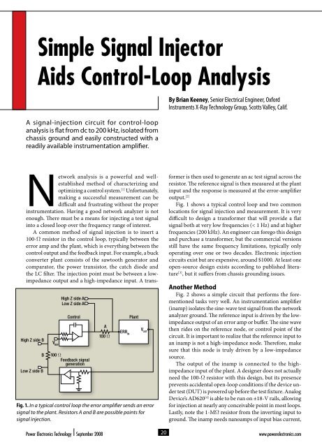
A common method of signal injection is to insert a<br />
100-W resistor in the control loop, typically between the<br />
error amp and the plant, which is everything between the<br />
control output and the feedback input. For example, a buck<br />
converter plant consists of the sawtooth generator and<br />
comparator, the power transistor, the catch diode and<br />
the LC filter. The injection point must be between a lowimpedance<br />
output and a high-impedance input. A trans-<br />
High Z side B<br />
B<br />
Low Z side B<br />
V REF<br />
High Z side A<br />
Low Z side A<br />
<strong>Control</strong><br />
100 W<br />
Feedback signal<br />
generation<br />
A<br />
100 W<br />
ERR IN<br />
Plant<br />
Fig. 1. In a typical control loop the error amplifier sends an error<br />
signal to the plant. Resistors A and B are possible points for<br />
signal injection.<br />
V OUT<br />
By Brian Keeney, Senior Electrical Engineer, Oxford<br />
Instruments X-Ray Technology Group, Scotts Valley, Calif.<br />
former is then used to generate an ac test signal across the<br />
resistor. The reference signal is then measured at the plant<br />
input and the response is measured at the error-amplifier<br />
output. [2]<br />
Fig. 1 shows a typical control loop and two common<br />
locations for signal injection and measurement. It is very<br />
difficult to design a transformer that will provide a flat<br />
signal both at very low frequencies (< 1 Hz) and at higher<br />
frequencies (200 kHz). An engineer can forego this design<br />
and purchase a transformer, but the commercial versions<br />
still have the same frequency limitations, typically only<br />
operating over one or two decades. Electronic injection<br />
circuits exist but are expensive, around $1000. At least one<br />
open-source design exists according to published literature<br />
[3] , but it suffers from chassis grounding issues.<br />
Another Method<br />
Fig. 2 shows a simple circuit that performs the forementioned<br />
tasks very well. An instrumentation amplifier<br />
(inamp) isolates the sine-wave test signal from the network<br />
analyzer ground. The reference input is driven by the lowimpedance<br />
output of an error amp or buffer. The sine wave<br />
then rides on the reference node, or control point of the<br />
circuit. It is important to realize that the reference input to<br />
an inamp is not a high-impedance node. Therefore, make<br />
sure that this node is truly driven by a low-impedance<br />
source.<br />
The output of the inamp is connected to the highimpedance<br />
input of the plant. A designer does not actually<br />
need the 100-W resistor with this design, but its presence<br />
prevents accidental open-loop conditions if the device under<br />
test (DUT) is powered up before the test fixture. Analog<br />
Device’s AD620 [4] is able to be run on ±18-V rails, allowing<br />
for injection at nearly any conceivable point in most loops.<br />
Lastly, note the 1-MW resistor from the inverting input to<br />
ground. The inamp needs nanoamps of input bias current,<br />
<strong>Power</strong> <strong>Electronics</strong> Technology September 2008 20<br />
www.powerelectronics.com
which isn’t much, but it is ill-advised to float the<br />
inputs completely. The resistor allows a very small<br />
amount of bias current without changing the return<br />
current paths appreciably.<br />
Design Verification<br />
J1-1<br />
The injection circuit was tested using a Venable<br />
3120 network analyzer. First, the open-circuit<br />
J1-2<br />
performance of the fixture was checked with a test<br />
voltage of 500 mV and the reference input biased at J1-3<br />
1 V (a graph of open-circuit performance is shown<br />
as Fig. A in the online version of this article.) The<br />
region of practical use is from 0 kHz to 200 kHz.<br />
The phase shift is unimportant because it affects<br />
neither the network measurement nor the DUT.<br />
However, gain is important because the injected<br />
signal will start to decrease in the region of gain<br />
roll-off, reducing signal-to-noise and resulting in<br />
an inferior measurement. A higher-performance<br />
inamp would extend the range of the circuit.<br />
It is very easy to believe erroneous results from a network<br />
analyzer. There are innumerable ways to compromise<br />
the measurement, from incorrect test signal amplitude to<br />
forgetting to turn on the injection circuit. It is important to<br />
have an oscilloscope hooked up to both the signal injection<br />
and measurement points. The signals should be relatively<br />
clean — distortion and noise compromise a reading. Once<br />
R2<br />
100 kW<br />
Low Z side<br />
Fig. 2. In the instrumentation amplifier-based signal injection circuit the<br />
output of the error amp drives the “low Z side”, and the “high Z side ” drives<br />
the plant input.<br />
the setup has passed an open-loop test like the one previously<br />
described, it is prudent to test a standard, such as a<br />
simple RC circuit. As a means of verifying signal integrity,<br />
a buffered 10-kW/16-nF low-pass filter was tested in the<br />
fixture with a dc bias of 1 V.<br />
Results of this test (see Fig. B in the online version of<br />
this article) showed that the performance was very good,<br />
matching the expected 3-dB point of 1 kHz. There are<br />
www.powerelectronics.com 21<br />
<strong>Power</strong> <strong>Electronics</strong> Technology September 2008<br />
R1<br />
10 kW<br />
R4<br />
1 MW<br />
+9 V<br />
+IN<br />
RG REF<br />
U1 +VS<br />
AD620<br />
RG –VS<br />
–IN –9V<br />
C1<br />
0.68 mF<br />
C2<br />
0.68 mF<br />
Output<br />
High Z side
50<br />
Gain (dB)<br />
–50<br />
1<br />
sigNAl iNjectioN<br />
Plant gain-gain<br />
Plant gain-phase<br />
Frequency (Hz)<br />
–180<br />
20 k<br />
Fig. 3. This closed-loop Bode plot of the high-voltage plant was<br />
obtained by placing the reference node (S1) of the analyzer at<br />
“high Z side A” and the measurement node (S2) at “low Z side B.”<br />
many other logical test circuits, but making a standard<br />
that closely matches the application is best. The results<br />
from a 10-Hz high-pass filter won’t yield much information<br />
about how the test circuit will behave at 100 kHz.<br />
Plant Measurement<br />
After verifying performance open loop and then in a<br />
test circuit, the test fixture was used to take practical data.<br />
The injection circuit was used to make actual network measurements<br />
of a 45-kV X-ray source’s kilovolt-drive circuit.<br />
This particular drive is for a handheld X-ray fluorescence<br />
spectrometer used in RoHS compliance testing. Because<br />
it is battery powered, the spectrometer needs to be stable<br />
over a rather wide input range of 12 V to18 V.<br />
Load conditions also vary widely, from 10 kV to 45 kV<br />
and 0 mA to 50 mA. The initial “guess” compensation worked<br />
well over most line and load conditions, but the supply occasionally<br />
oscillated at high kilovolt and no load. To find<br />
out what was going wrong, the inamp test fixture was used<br />
to probe stability at several line and load combinations,<br />
including the problem region.<br />
Even if the compensation is in place and working, it is<br />
usually very instructive to first look at the plant response.<br />
Run the system closed loop and place the test input at the<br />
input of the plant, but instead of placing the measurement<br />
input at the output of the error amp, place it at the output<br />
of the feedback generation circuit (or the output of the<br />
plant).<br />
A 100-W resistor was inserted between the error amp<br />
and the plant, and the injector was connected as previously<br />
described. The reference input of the network analyzer was<br />
connected to the output of the inamp, and the signal input<br />
of the network analyzer was connected to the buffered<br />
feedback reference (1 V = 10 kV). The DUT was brought<br />
up to 45 kV and 40 mA of load current, and the injected<br />
sine-wave amplitude was adjusted to yield a good signal,<br />
but not so much as to disrupt the operating point (about<br />
180<br />
Phase (degrees)<br />
Frequency (Hz)<br />
Fig. 4. A type-2 integrator was used to stabilize the loop in a<br />
typical Bode plot of the high-voltage supply’s loop gain. Phase<br />
margin in this supply is 60 degrees, which ensures that the<br />
supply doesn’t overshoot, but at the expense of settling time.<br />
100 mV PK-PK ). A sweep from 1 Hz to 20 kHz yielded the<br />
results in Fig. 3.<br />
By knowing that a type-1 integrating error amplifier<br />
provides a constant 270 degrees of phase shift (90 degrees<br />
from the capacitor and 180 degrees from the logic inversion<br />
of the amp), the phase can be shifted to see where the<br />
0 degree crossing point is. The criterion for stability is that<br />
the gain must be less than 0 dB when the phase crosses<br />
0 degrees. Knowing this, the integrator roll-off can be set<br />
for optimal performance.<br />
The measurement described previously was repeated<br />
for several line and load conditions. It was found that the<br />
dip in phase shown in Fig. 4 shifted to lower frequencies<br />
with decreasing load. This effect was so pronounced that<br />
the ample phase margin at 45 kV and 50 mA was reduced<br />
to zero at no load, leading to the oscillation described<br />
previously. H. Dean Venable wrote a landmark paper on<br />
optimizing feedback compensation networks. [1] Through<br />
use of the techniques prescribed by Venable, the phase in<br />
that area was boosted to ensure stability over all line and<br />
load conditions.<br />
Note that there are two practical ways to make this<br />
plant measurement. The loop usually can be stabilized by<br />
swamping the capacitance of the integrator. Even if the<br />
dynamic performance is abominable, it will keep the plant<br />
in the operating region so that the designer can perform the<br />
forementioned test. Once the test is complete, the designer<br />
can calculate the optimal compensation and tune the error<br />
amp to a stable, high-performance state.<br />
A second way to perform this measurement is to run<br />
the plant open loop, using a variable voltage reference to<br />
set the operating point. This dc level is injected into the<br />
reference input of the inamp, and the output of the inamp<br />
drives the plant directly. On pulse-width modulation chips<br />
with internal amps, this node is often available as the COMP<br />
pin. Running the chip in this configuration can be a little<br />
<strong>Power</strong> <strong>Electronics</strong> Technology September 2008 22<br />
www.powerelectronics.com<br />
50<br />
Gain (dB)<br />
-50<br />
1<br />
Plant gain-gain<br />
Plant gain-phase<br />
Slide bar:<br />
357.2 Frequency (Hz)<br />
0 Gain (dB)<br />
58.12 Phase (degrees)<br />
-2.47 Slope (20 dB/decade)<br />
180<br />
Phase (degrees)<br />
-180<br />
20 k
sigNAl iNjectioN<br />
tricky since ICs such as Linear Technology’s LT3431 [5] pack<br />
a bunch of features into the feedback node, for example<br />
frequency reduction and current limiting. Clamping the<br />
feedback input to the correct voltage will often solve these<br />
problems (e.g., in the case of the LT3431, a voltage of 1 V<br />
keeps the chip operating normally). [5]<br />
<strong>Loop</strong> Measurement<br />
The Bode plot in Fig. 3 shows a plant gain of about 11 dB<br />
and a 90 degree phase shift at about 1.5 kHz. Using Venable’s<br />
methods, the loop was compensated to have 60 degrees of<br />
phase margin (the phase at the 0-dB point). This results in<br />
a slightly overdamped response to step changes in program,<br />
which minimizes the voltage stress on the components. In<br />
other systems, fast settling time might be more important,<br />
which would indicate a lower phase margin, but resulting<br />
in more overshoot.<br />
Fig. 4 shows the Bode plot of the compensated power<br />
supply at 45 kV and 50 mA. The results of the test match the<br />
DUT connections (banana cables)<br />
Aux amp connections<br />
BNC from N.A.<br />
J4-1<br />
J4-2<br />
J5-1<br />
J5-2<br />
J6-1<br />
J6-2<br />
J8-1<br />
J8-2<br />
J9-1<br />
J9-2<br />
J1-1<br />
J1-2<br />
J1-3<br />
R2<br />
100 kW<br />
Low Z<br />
side<br />
High Z<br />
side<br />
Aux in<br />
Aux in<br />
Aux out<br />
BNC to S1<br />
R11<br />
No load<br />
J10-1<br />
J10-2<br />
J10-3<br />
+<br />
J2-8<br />
-<br />
R12<br />
100 kW<br />
C3<br />
100 pF<br />
Low Z side<br />
10x, 100x Attenuation<br />
R1<br />
10 kW<br />
J2-1<br />
J2-2<br />
R3<br />
1 kW<br />
J3-1<br />
J3-2<br />
R4<br />
1 MW<br />
LT1057<br />
High Z<br />
side<br />
Aux out<br />
+IN<br />
RG REF<br />
RG<br />
–IN<br />
U1<br />
AD620<br />
BNC to S2<br />
+9 V<br />
OUTPUT<br />
J11-1<br />
J11-2<br />
J11-3<br />
LM4D4D, 2.5 V LM4C4C, 2.5 V<br />
+V5<br />
–V5<br />
–9 V<br />
+9 V<br />
D2<br />
NC<br />
NC<br />
C2<br />
0.68 mF<br />
C1<br />
0.68 mF<br />
-9 V<br />
predicted response of the measured plant gain combined<br />
with the integrator, indicating that the test fixture performs<br />
its task well.<br />
Network analysis can be difficult not only because of the<br />
challenges of signal injection, but also due to the practical<br />
difficulties of maneuvering so many test leads and scope<br />
probes. It is very easy to short out a critical point and destroy<br />
equipment or the DUT. The test jig described next<br />
and pictured in the online version of this article overcomes<br />
many of these challenges.<br />
Fig. 5 shows the full schematic of the signal injection<br />
circuit. In the upper left-hand corner, U1 handles the<br />
actual signal injection. Note that there is isolation from<br />
chassis ground at the signal input. R4 provides enough<br />
current for input bias current requirements, but shouldn’t<br />
cause ground loop errors. Jumpers J2 and J3 provide 10x<br />
and 100x attenuation for fine control of the injected signal,<br />
which can be very helpful for analyzers with limited<br />
attenuation control. Two batteries provide low noise and<br />
Fig. 5. Complete schematic of signal-injection pc board. The inamp in the upper left-hand corner does the actual signal injection.<br />
R8<br />
10 kW<br />
D3<br />
Low Z side<br />
R7<br />
10 kW<br />
High Z side<br />
<strong>Power</strong> <strong>Electronics</strong> Technology September 2008 24<br />
www.powerelectronics.com<br />
R5<br />
CW<br />
LED +9 V<br />
+9 V<br />
-9 V 5W1<br />
DPDT switch<br />
R6<br />
5 kW<br />
D1<br />
<strong>Power</strong> on<br />
R10<br />
5 kW<br />
R11<br />
4 kW<br />
REF for Open-loop plant analysis<br />
+ LT1057<br />
U2-A<br />
-<br />
R14<br />
100 kW<br />
C4<br />
100 pF<br />
R16<br />
100 kW<br />
V+<br />
V-<br />
V+<br />
V-<br />
+9 V<br />
J7-2<br />
J7-1<br />
B1<br />
9-V holder<br />
B2<br />
9-V holder<br />
R15<br />
5kW<br />
D5<br />
TL431<br />
R9<br />
5kW<br />
D4<br />
Low battery (< 7.5 V)<br />
Q1<br />
Low Z side
isolated rails (this could be changed to extend the usable<br />
range to ±18 V).<br />
In the lower right-hand corner, U2 (LT1057) provides<br />
buffering for a variable voltage reference (needed for making<br />
open-plant measurements) and an auxiliary buffer (for<br />
providing a low-impedance feedback point). To make the<br />
open-plant measurements, J7 is jumpered and the pot adjusted<br />
until the plant is at the desired operating point. The<br />
plant response is then measured from “high Z side A” to<br />
“low Z side B” (Fig. 1). The TL431 is used for a low-batterydetect<br />
circuit. The various connectors are used to interface<br />
between the DUT and the network analyzer.<br />
The fixture’s mechanical layout is<br />
nearly as important as its electrical<br />
functionality. (A mechanical layout of<br />
the pc board appears as Fig. C in the<br />
online version of this article.) Three BNC<br />
connections at the back of the board go<br />
off to the network analyzer (sine, reference,<br />
measurement). This keeps all the<br />
large cables out of the way and under<br />
control. Two 9-V batteries (mounted<br />
on the underside of the board) provide<br />
power, eliminating another piece of test<br />
equipment from the designer’s bench.<br />
Additionally, the batteries provide some<br />
mass, which is needed to keep the board<br />
from falling off the bench.<br />
Three banana jacks are mounted at the<br />
front of the board. These connect to the<br />
DUT ground and the low-impedance and<br />
high-impedance sides of the resistor. The<br />
resistor should be on the DUT and should<br />
preferably be built in to the pc board.<br />
There is negligible cost or mass penalty<br />
to one extra resistor in the assembly. Test<br />
points on either side of the resistor are<br />
extremely helpful for clipping in both the<br />
banana test leads and the scope probes.<br />
A three-pin SIP header is very useful for<br />
connecting all three signals at once.<br />
When making plant measurements,<br />
the banana leads stay as they are, but the<br />
measurement BNC is unplugged, and the<br />
measurement test node is probed directly<br />
from the network analyzer to the node of<br />
interest on the DUT. Other useful user<br />
features on the board include a poweron<br />
LED and a low-battery LED. Both are<br />
very helpful at preventing measurement<br />
errors. PETech<br />
References<br />
1. Venable, H. Dean. “Optimum Feedback<br />
Amplifier Design for <strong>Control</strong> Systems,”<br />
Proceedings of Intersociety Energy Con-<br />
version Engineering Conference, August 1986.<br />
2. Venable, H. Dean. “Practical Testing Techniques for<br />
Modern <strong>Control</strong> <strong>Loop</strong>s,” Venable Industries Technical<br />
Paper #16, www.venable.biz.<br />
3. Galinski, Martin. “Use Op-Amp Injection for Bode<br />
<strong>Analysis</strong>,” EDN, Sept. 16, 2004, pp. 90, 92.<br />
4. “AD620: Low Drift, Low <strong>Power</strong> Instrumentation Amp<br />
with Set Gains of 1 to 10000,” Analog Devices data sheet,<br />
www.analog.com.<br />
5. “LT3431: High Voltage, 3A, 500kHz Step-Down Switching<br />
Regulator,” Linear Technology Datasheet, www.linear.<br />
com.<br />
Visit our all-new website and you'll find answers to all of<br />
your capacitor sourcing needs faster than ever before!<br />
Best of all, the Illinois Capacitor website is backed by real live<br />
capacitor experts, ready to help you design-in and source the<br />
best possible capacitors.<br />
• All new, expanded site!<br />
• Search by type, parameter,<br />
part number or application!<br />
• Print detailed spec sheets<br />
• Request samples, quotes<br />
and catalogs<br />
• Complete PDF's of the<br />
latest catalog<br />
• Search live distributor<br />
inventories and more<br />
• Lastest RoHS and ISO<br />
documents<br />
• Life calculators, formulas,<br />
glossary of terms, papers<br />
and application notes<br />
Log on today,<br />
Bookmark it for tomorrow!<br />
(847) 675-1760<br />
FAX (847) 673-2850<br />
sales@illcap.com<br />
www.powerelectronics.com 25<br />
<strong>Power</strong> <strong>Electronics</strong> Technology September 2008