here. - Power Electronics
here. - Power Electronics
here. - Power Electronics

You also want an ePaper? Increase the reach of your titles
YUMPU automatically turns print PDFs into web optimized ePapers that Google loves.
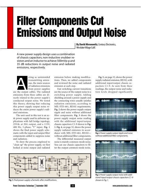
Filter Components Cut<br />
Emissions and Output Noise<br />
A new power supply design uses a combination<br />
of chassis capacitors, non-inductive snubber resistors<br />
and an inductor to achieve 500mVp-p and<br />
35 dB reductions in output noise and radiated<br />
emissions, respectively.<br />
Acting as unintended<br />
transmitting antennae,<br />
the main sources<br />
of radiation emissions<br />
from power supplies<br />
are the output cables. The radiated<br />
emissions from these cables are directly<br />
related to the power supply’s<br />
conducted output noise. We tested<br />
this theory, showing that reducing<br />
this power supply output noise reduces<br />
the entire power supply’s radiated<br />
emissions.<br />
The unit used in this test is an acdc<br />
power supply used in airborne applications<br />
with full bridge topology,<br />
25Vdc at 20A output, and a 115V,<br />
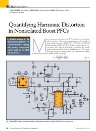
400 Hz, 3-phase, “Y” input. Fig. 1<br />
shows the final power supply schematic<br />
with the input and output filter<br />
components added to suppress noise<br />
and radiation.<br />
To show the process employed to<br />
“clean up” the power supply, we first<br />
looked at noise output and radiated<br />
Fig. 1. Final power supply schematic after modifications.<br />
emission before making modifications.<br />
Then, we added components<br />
and reviewed the noise and radiated<br />
emission at each step.<br />
Fast switching current transitions<br />
are the source of the output noise in a<br />
switching power supply. Adding<br />
shielding around a power supply and<br />
the connecting wires usually satisfies<br />
radiation emissions, according to<br />
MIL-STD-461, RE102 requirements.<br />
Fig. 2 shows the power supply output<br />
ripple and noise without additional<br />
filter components. Fig. 3 shows the<br />
power supply output noise reading<br />
with the additional input/output<br />
chassis capacitors C1-9 shown in Fig.<br />
1. Fig. 4, on page 32, shows the power<br />
supply radiated emission in accordance<br />
with MIL-STD-461, RE102—<br />
without additional filter components.<br />
The differential measured output<br />
noise is mainly common-mode noise.<br />
You can use chassis capacitors to filter<br />
the output common-mode noise.<br />
By David Ahronowitz, Century <strong>Electronics</strong>,<br />
Westlake Village Calif.<br />
Fig. 5, on page 32, shows the power<br />
supply radiated emission, RE102, with<br />
additional input/output chassis capacitors<br />
C1-9. As seen from these<br />
readings, the output noise and radiation<br />
levels dropped significantly<br />
Fig. 2. <strong>Power</strong> supply output ripple and noise<br />
without additional filter components.<br />
Fig. 3. <strong>Power</strong> supply output noise with additional<br />
input/output chassis capacitors C1-9<br />
shown in Fig. 1.<br />
<strong>Power</strong> <strong>Electronics</strong> Technology September 2002 30<br />
www.powerelectronics.com
NOISE/EMISSIONS<br />
Fig. 4. <strong>Power</strong> supply radiated emission without additional filter<br />
components.<br />
(465mVp-p and 20dB).<br />
A non-inductive wire-wound resistor used in an RC<br />
output rectifier snubber can reduce the turn-off spike affectivity.<br />
Fig. 6 shows the power supply radiated emission,<br />
RE102, with additional input/output capacitors C1-9 and<br />
non-inductive snubber resistors R1 and R2. These results<br />
show 10mVp-p and 6dB noise reduction compared with<br />
TANCERAM<br />
Ceramic MLCCs for<br />
Tantalum Replacement<br />
®<br />
ESR (ohms)<br />
1<br />
0.1<br />
1.0 µF<br />
Tantalum<br />
1.0 µF<br />
TANCERAM ®<br />
0.01<br />
0.1 1 10 100<br />
Frequency (MHz)<br />
• Better high frequency ESR<br />
• 400% higher breakdown voltage<br />
• Smaller size: 0805, 0603, & 0402<br />
Visit us at the<br />
• Lower leakage current<br />
• No component polarity<br />
CIRCLE 222 on Reader Service Card<br />
Booth #1636<br />
Visit our website today for complete details<br />
johanson dielectrics.com<br />
sylmar california 818.364.9800<br />
®<br />
Fig. 5. <strong>Power</strong> supply radiated emission with additional input/output<br />
chassis capacitors C1-9.<br />
those observed in Fig. 3 and 5.<br />
A common-mode inductor together with the chassis<br />
capacitors form a good output filter and provide a return<br />
path for the common-mode noise. Looking at Fig. 7, you’ll<br />
see the power supply radiated emission, RE102, with<br />
additional input/output capacitors C1-9, non-inductive<br />
snubber resistors R1 and R2 and common-mode output<br />
Fig. 6. <strong>Power</strong> supply radiated emission with additional input/output<br />
capacitors C1-9 and non-inductive snubber resistors R1 and R2.<br />
Fig. 7. <strong>Power</strong> supply radiated emission with additional input/output<br />
capacitors C1-9, non-inductive snubber resistors R1 and R2 and<br />
common-mode output inductor L1.<br />
<strong>Power</strong> <strong>Electronics</strong> Technology September 2002 32<br />
www.powerelectronics.com
inductor L1.<br />
Fig. 8 shows the power supply output<br />
noise with additional input/output<br />
chassis capacitors C1-9 and<br />
non-inductive snubber resistors R1<br />
and R2. Fig. 9 shows the power supply<br />
output noise with additional input/output<br />
chassis capacitors C1-9,<br />
non-inductive snubber resistors R1<br />
and R2 and common-mode output<br />
inductor L1.<br />
These results show that in combination,<br />
these three modifications to<br />
Fig. 8. <strong>Power</strong> supply output noise with additional<br />
input/output chassis capacitors C1-9 and noninductive<br />
snubber resistors R1 and R2.<br />
Fig. 9. <strong>Power</strong> supply output noise with<br />
additional input/output chassis capacitors C1-<br />
9, non-inductive snubber resistors R1 and R2<br />
and common-mode output inductor L1.<br />
the circuit reduce output noise by<br />
about 500mVp-p, and in the process<br />
reduce radiated emissions by about 35<br />
dB at 50 MHz.<br />
During the power supply development,<br />
even if the power supply<br />
meets the output noise specification<br />
requirements, it’s important to further<br />
reduce the power supply output<br />
noise. As we have seen, a power<br />
supply with low output noise will<br />
help the system meet the radiation<br />
emission requirements during the<br />
system qualification without the<br />
need for additional shielding<br />
around the power supply or the connecting<br />
cables.<br />
This unshielded power supply<br />
Visit us at the<br />
Booth #1325<br />
®<br />
CIRCLE 223 on Reader Service Card<br />
NOISE/EMISSIONS<br />
didn’t fully meet the MIL-STD-461,<br />
RE102 limits, when initially installed.<br />
However, the final system<br />
did meet the radiation emissions requirements<br />
after making the filtering<br />
modifications. PETech<br />
For more information on this article,<br />
CIRCLE 332 on Reader Service Card<br />
www.powerelectronics.com 33<br />
<strong>Power</strong> <strong>Electronics</strong> Technology September 2002