S-300u Series - Swissbit
S-300u Series - Swissbit
S-300u Series - Swissbit

You also want an ePaper? Increase the reach of your titles
YUMPU automatically turns print PDFs into web optimized ePapers that Google loves.
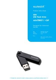
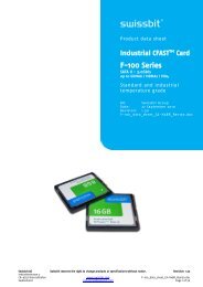
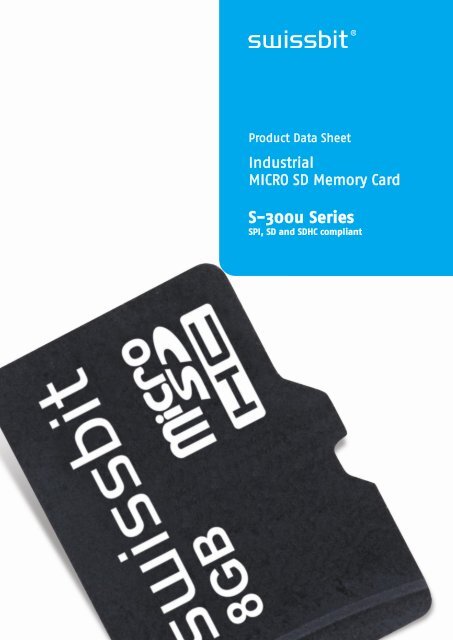
Product Data Sheet<br />
Industrial<br />
MICRO SD Memory Card<br />
S-<strong>300u</strong> <strong>Series</strong><br />
SPI, SD and SDHC compliant<br />
<strong>Swissbit</strong> AG <strong>Swissbit</strong> reserves the right to change products or specifications without notice. Revision: 1.00<br />
Industriestrasse 4<br />
CH-9552 Bronschhofen www.swissbit.com S-<strong>300u</strong>_data_sheet_Rev100.doc<br />
Switzerland industrial@swissbit.com Page 19 of 19
S-<strong>300u</strong> <strong>Series</strong><br />
MICRO SD Memory Card<br />
1 Feature summary<br />
Highly-integrated memory controller<br />
o Fully compliant with SD Memory Card specification SD1.01, SD1.1, SD2.0<br />
and SD3.01 and MICRO SD Memory Card Addendum 4.00<br />
Standard MICRO SD Memory Card form factor<br />
o 15.0mm x 11.0mm x 0.7mm<br />
Operating voltage 2.7…3.6V<br />
Low-power CMOS technology<br />
High reliability<br />
o MTBF: > 3,000,000 hours<br />
o Number of insertions: > 10,000<br />
o Extended Temperature range -25° up to 85°C<br />
Hot swappable<br />
High performance<br />
o Speed class<br />
2GB Card class 6<br />
4GB to 8GB class 10<br />
o SD burst up to 25MB/s<br />
o SD Low speed 0…25MHz clock rate<br />
o SD High speed 25…50MHz clock rate<br />
o Flash burst up to 40MB/s<br />
o Flash Bus interleave<br />
Operating bus modes: SD 1 & 4bit and SPI<br />
Error Correction up to 24bit/1KB BCH ECC<br />
Wear Leveling: equal wear leveling of static and dynamic data<br />
The wear leveling assures that dynamic data as well as static data is balanced evenly across the memory.<br />
With that the maximum write endurance of the device is guaranteed.<br />
Write Endurance: Due to advanced wear leveling an even use of the entire flash is guaranteed, regardless<br />
how much “static” (OS) data is stored. Example: If the average file size is 10MByte and the total capacity is<br />
8GByte, 48Mio write cycles can be performed.<br />
Available densities<br />
o 2, 4 and 8GBytes (SLC NAND Flash)<br />
Controlled BOM<br />
Life Cycle Management<br />
2 Order Information<br />
2.1 Standard product list<br />
Table 1: Standard Product List<br />
Density Part Number<br />
2GB SFSD2048NgBW1MT-E-ME-1x1-STD<br />
4GB SFSD4096NgBW1MT-E-DF-1x1-STD<br />
8GB SFSD8192NgBW1MT-E-QG-1x1-STD<br />
g defines the product generation<br />
x defines the FW<br />
2.2 Current product generation<br />
Table 2: Standard Product List<br />
Density Part Number<br />
2GB SFSD2048N1BW1MT-E-ME-111-STD<br />
4GB SFSD4096N1BW1MT-E-DF-111-STD<br />
8GB SFSD8192N1BW1MT-E-QG-111-STD<br />
<strong>Swissbit</strong> AG <strong>Swissbit</strong> reserves the right to change products or specifications without notice. Revision: 1.00<br />
Industriestrasse 4<br />
CH-9552 Bronschhofen www.swissbit.com S-<strong>300u</strong>_data_sheet_Rev100.doc<br />
Switzerland industrial@swissbit.com Page 19 of 19
3 Contents<br />
1 FEATURE SUMMARY ..................................................................................................................................................................... 2<br />
2 ORDER INFORMATION .................................................................................................................................................................. 2<br />
2.1 STANDARD PRODUCT LIST .......................................................................................................................................................... 2<br />
2.2 CURRENT PRODUCT GENERATION ................................................................................................................................................ 2<br />
3 CONTENTS .................................................................................................................................................................................... 3<br />
4 PRODUCT SPECIFICATION ............................................................................................................................................................. 4<br />
4.1 SYSTEM PERFORMANCE ............................................................................................................................................................ 4<br />
4.2 ENVIRONMENTAL SPECIFICATIONS .............................................................................................................................................. 4<br />
4.2.1 Recommended Operating Conditions ............................................................................................................... 4<br />
4.2.2 Recommended Storage Conditions ................................................................................................................... 5<br />
4.2.3 Humidity & ESD .................................................................................................................................................... 5<br />
4.2.4 Environmental Conditions ................................................................................................................................. 5<br />
4.3 PHYSICAL DIMENSIONS ............................................................................................................................................................ 5<br />
4.4 RELIABILITY .......................................................................................................................................................................... 5<br />
5 CAPACITY SPECIFICATION ............................................................................................................................................................. 5<br />
6 CARD PHYSICAL ........................................................................................................................................................................... 6<br />
6.1 PHYSICAL DESCRIPTION ............................................................................................................................................................ 6<br />
7 ELECTRICAL INTERFACE ................................................................................................................................................................ 7<br />
7.1 ELECTRICAL DESCRIPTION ........................................................................................................................................................... 7<br />
7.2 DC CHARACTERISTICS ............................................................................................................................................................... 8<br />
7.3 SIGNAL LOADING .................................................................................................................................................................... 8<br />
7.4 AC CHARACTERISTICS ............................................................................................................................................................... 9<br />
8 HOST ACCESS SPECIFICATION ......................................................................................................................................................11<br />
8.1 SD AND SPI BUS MODES .......................................................................................................................................................11<br />
8.1.1 SD Bus Mode Protocol .........................................................................................................................................11<br />
8.1.2 SPI Bus Mode Protocol ........................................................................................................................................12<br />
8.1.3 Mode Selection ....................................................................................................................................................12<br />
8.2 CARD REGISTERS...................................................................................................................................................................13<br />
9 PART NUMBER DECODER ............................................................................................................................................................16<br />
9.1 MANUFACTURER ....................................................................................................................................................................16<br />
9.2 MEMORY TYPE .....................................................................................................................................................................16<br />
9.3 PRODUCT TYPE .....................................................................................................................................................................16<br />
9.4 CAPACITY ............................................................................................................................................................................16<br />
9.5 PLATFORM ..........................................................................................................................................................................16<br />
9.6 GENERATION .......................................................................................................................................................................16<br />
9.7 MEMORY ORGANIZATION ........................................................................................................................................................16<br />
9.8 TECHNOLOGY .......................................................................................................................................................................16<br />
9.9 CHANNELS ..........................................................................................................................................................................16<br />
9.10 FLASH CODE .......................................................................................................................................................................16<br />
9.11 TEMP. OPTION ....................................................................................................................................................................17<br />
9.12 DIE CLASSIFICATION .............................................................................................................................................................17<br />
9.13 PIN MODE ........................................................................................................................................................................17<br />
9.14 CONFIGURATION XYZ ...........................................................................................................................................................17<br />
9.15 OPTION .............................................................................................................................................................................17<br />
10 SWISSBIT LABEL SPECIFICATION ................................................................................................................................................18<br />
10.1 FRONT SIDE MARKING ...........................................................................................................................................................18<br />
10.2 BACK SIDE MARKING ............................................................................................................................................................18<br />
11 REVISION HISTORY .....................................................................................................................................................................19<br />
<strong>Swissbit</strong> AG <strong>Swissbit</strong> reserves the right to change products or specifications without notice. Revision: 1.00<br />
Industriestrasse 4<br />
CH-9552 Bronschhofen www.swissbit.com S-<strong>300u</strong>_data_sheet_Rev100.doc<br />
Switzerland industrial@swissbit.com Page 19 of 19
4 Product Specification<br />
The MICRO SD Memory Card is a small form factor non-volatile memory card which provides high capacity data<br />
storage. Its aim is to capture, retain and transport data, audio and images, facilitating the transfer of all types of<br />
digital information between a large variety of digital systems.<br />
The card operates in two basic modes:<br />
SD/SDHC card mode<br />
SPI mode<br />
The MICRO SD Memory Card also supports SD High Speed mode with up to 50MHz clock frequency.<br />
The cards are compliant with<br />
SD Memory card Specification Part 1, Physical layer Specification V3.01<br />
SD Memory card Specification Part 2, File System Specification V3.00<br />
SD Memory card Specification Part 3, Security Specification V3.00<br />
MICRO SD Memory Card Addendum V4.00<br />
Simplified specifications are available at https://www.sdcard.org/downloads/pls/simplified_specs/<br />
The Card has an internal intelligent controller which manages interface protocols, data storage and retrieval as<br />
well as hardware BCH Error Correction Code (ECC), defect handling, diagnostics and clock control.<br />
The advanced wear leveling mechanism assures an equal usage of the Flash memory cells to extend the life time.<br />
The hardware BCH-code ECC allows to detect and correct up to 24 defect bits per 1kByte.<br />
The card has a power-loss management feature to prevent data corruption after power-down. The power<br />
consumption is very low.<br />
The cards are RoHS compliant and lead-free.<br />
4.1 System Performance<br />
Table 3: Performance<br />
System Performance typ max Unit<br />
Burst Data transfer Rate (max SD clock 50MHz) 25<br />
2GB 19 (1)(2) 24 (1)(3)<br />
Sustained Sequential Read<br />
4…8GB 19 MB/s<br />
(1)(2) 24 (1)(3)<br />
Sustained Sequential Write<br />
2GB 11 (1)(2) 12 (1)(3)<br />
4…8GB 17 (1)(2) 22 (1)(3)<br />
1. All values refer to Micron Flash 8Gb MICRO SD Memory Card in SD mode 50MHz, cycle time 20ns,<br />
2. Sustained Speed measured with USB-SD Memory Card reader. It depends on burst speed, flash number, and file size.<br />
3. Maximum values were measured with Testmetrix tester.<br />
4.2 Environmental Specifications<br />
4.2.1 Recommended Operating Conditions<br />
Table 4: MICRO SD Memory Card Recommended Operating Conditions<br />
Parameter min typ max unit<br />
Extended Operating Temperature -25 25 85 °C<br />
Power Supply VCC (3.3V) 2.7 3.3 3.6 V<br />
Table 5: Current consumption<br />
Current Consumption (typ) typ max Unit<br />
Write 60 70<br />
Read 50 60<br />
mA<br />
Sleep Mode 0.15 2<br />
<strong>Swissbit</strong> AG <strong>Swissbit</strong> reserves the right to change products or specifications without notice. Revision: 1.00<br />
Industriestrasse 4<br />
CH-9552 Bronschhofen www.swissbit.com S-<strong>300u</strong>_data_sheet_Rev100.doc<br />
Switzerland industrial@swissbit.com Page 19 of 19
4.2.2 Recommended Storage Conditions<br />
Table 6: MICRO SD Memory Card Recommended Storage Conditions<br />
Parameter min typ max unit<br />
Extended Storage Temperature -25 25 85 °C<br />
4.2.3 Humidity & ESD<br />
Table 7: Humidity & ESD<br />
Parameter Operating Non Operating<br />
Humidity (non-condensing) operation: 95% RH @25°C<br />
storage: 93% RH @40°C, 500h<br />
EMC / EMI Non Contact Pads area:<br />
±8 kV (air discharge)<br />
Human body model according<br />
to IEC61000-4-2<br />
Contact Pads:<br />
±4 kV, Human body model<br />
according to IEC61000-4-2<br />
4.2.4 Environmental Conditions<br />
Table 8: Environmental Conditions<br />
Parameter Operating Non Operating<br />
UV light exposure UV: 254nm, 15Ws/cm 2 according to ISO7816-1<br />
Durability 10,000 mating cycles<br />
Drop test 1.5m free fall<br />
Bending / Torque 10N / 0.10Nm ±2.5° max<br />
4.3 Physical Dimensions<br />
Table 9: Physical Dimensions<br />
Outer Physical Dimensions Value Unit<br />
Length 15.0±0.1<br />
Width 11.0±0.1<br />
mm<br />
Thickness 0.7 (1.0)±0.1<br />
Weight (typ.) 0.4 g<br />
4.4 Reliability<br />
Table 10: Reliability<br />
Parameter Value<br />
Data Retention @ 25°C 10 years (JEDEC47G)<br />
5 Capacity specification<br />
Table 11: MICRO SD Memory Card capacity specification<br />
Capacity Sectors Total addressable capacity (Byte)<br />
2GB 4’016’128 2’056’257’536<br />
4GB 8’042’496 4’117’757’952<br />
8GB 16’136’192 8’261’730’304<br />
<strong>Swissbit</strong> AG <strong>Swissbit</strong> reserves the right to change products or specifications without notice. Revision: 1.00<br />
Industriestrasse 4<br />
CH-9552 Bronschhofen www.swissbit.com S-<strong>300u</strong>_data_sheet_Rev100.doc<br />
Switzerland industrial@swissbit.com Page 19 of 19
6 Card physical<br />
6.1 Physical description<br />
The MICRO SD Memory Card contains a single chip controller and Flash memory module(s). The controller interfaces<br />
with a host system allowing data to be written to and read from the Flash memory module(s).<br />
Figure 1 and Figure 2 show card dimensions.<br />
Figure 1: Mechanical Dimensions MICRO SD<br />
Memory Card (side and top, simplified)<br />
Figure 2: Mechanical Dimensions MICRO SD<br />
Memory Card (bottom side with connector)<br />
<strong>Swissbit</strong> AG <strong>Swissbit</strong> reserves the right to change products or specifications without notice. Revision: 1.00<br />
Industriestrasse 4<br />
CH-9552 Bronschhofen www.swissbit.com S-<strong>300u</strong>_data_sheet_Rev100.doc<br />
Switzerland industrial@swissbit.com Page 19 of 19
7 Electrical interface<br />
7.1 Electrical description<br />
Figure 3: MICRO SD Memory Card Block Diagram<br />
Figure 4: MICRO SD Memory Card Shape and<br />
Interface (Bottom View)<br />
Table 12: MICRO SD Memory Card Pad Assignment<br />
Pin # SD Mode SPI Mode<br />
Name Type 1 Description Name Type 1 Description<br />
1 DAT2 5 I/O/PP Data Line [Bit 2] RSV<br />
2 CD/DAT3 2 I/O/PP 3 Card Detect/ Data Line [Bit 3] CS I 3 Chip Select (negative true)<br />
3 CMD PP Command/Response DI I Data In<br />
4 VDD S Supply voltage VDD S Supply voltage<br />
5 CLK I Clock SCLK I Clock<br />
6 VSS S Supply voltage ground VSS S Supply voltage ground<br />
7 DAT0 I/O/PP Data Line [Bit 0] DO O/PP Data Out<br />
8 DAT1 4 I/O/PP Data Line [Bit 1] RSV<br />
Notes:<br />
1) S: power supply; I: input; O: output using push-pull drivers; PP: I/O using push-pull drivers;<br />
2) The extended DAT lines (DAT1-DAT3) are input on power up. They start to operate as DAT lines after<br />
SET_BUS_WIDTH command. The Host shall keep its own DAT1-DAT3 lines in input mode, as well, while they<br />
are not used.<br />
3) At power up this line has a 50kOhm pull up enabled in the card. This resistor serves two functions Card<br />
detection and Mode Selection. For Mode Selection, the host can drive the line high or let it be pulled high<br />
to select SD mode. If the host wants to select SPI mode it should drive the line low. For Card detection,<br />
the host detects that the line is pulled high. This pull-up should be disconnected by the user, during<br />
regular data transfer, with SET_CLR_CARD_DETECT (ACMD42) command<br />
4) DAT1 line may be used as Interrupt Output (from the Card) in SDIO mode during all the times that it is not<br />
in use for data transfer operations (refer to "SDIO Card Specification" for further details).<br />
5) DAT2 line may be used as Read Wait signal in SDIO mode (refer to "SDIO Card Specification" for further<br />
details).<br />
<strong>Swissbit</strong> AG <strong>Swissbit</strong> reserves the right to change products or specifications without notice. Revision: 1.00<br />
Industriestrasse 4<br />
CH-9552 Bronschhofen www.swissbit.com S-<strong>300u</strong>_data_sheet_Rev100.doc<br />
Switzerland industrial@swissbit.com Page 7 of 19
7.2 DC characteristics<br />
Measurements are at Recommended Operating Conditions unless otherwise specified.<br />
Table 13: DC Characteristics<br />
Symbol Parameter min typ max unit notes<br />
Peak Voltage on all Lines -0.3 VDD+0.3 V<br />
VIL Input LOW Voltage -0.3 0.25*VDD V<br />
VIH Input HIGH Voltage 0.625*VDD VDD+0.3 V<br />
VOL Output LOW Voltage 0.125*VDD V at 100µA<br />
VOH Output HIGH Voltage 0.75*VDD V at 100µA<br />
Operating Current 35 50 mA<br />
IDD Pre-initialization Standby Current 3 mA<br />
Post-initialization Standby Current 100 200 µA<br />
ILI Input Leakage Current -10 10 µA without<br />
ILO Output Leakage Current -10 10 µA pull up R<br />
Table 14: MICRO SD Memory Card Recommended Operating Conditions<br />
Symbol Parameter min typ max unit<br />
Normal Operating Status 2.7 3.6 V<br />
VDD Supply Voltage Basic Communication<br />
(CMD0, CMD15, CMD55, ACMD41)<br />
2.0 3.3 3.6 V<br />
- Power Up Time (from 0V to VDD min) 250 ms<br />
7.3 Signal Loading<br />
The total capacitance C L is the sum of the bus master capacitance C HOST, the bus capacitance C BUS, and the<br />
capacitance C CARD of the card connected to the line:<br />
C L = C HOST + C BUS + C CARD<br />
To allow the sum of the host and bus capacitances to be up to 20pF for the card, the following conditions in the<br />
table below are met by the card.<br />
Table 15: Signal loading<br />
Parameter Symbol Min Max Unit Notes<br />
Pull up resistance R CMD 10 100 kOhm To prevent bus floating<br />
Pull up resistance R DAT 10 100 kOhm To prevent bus floating<br />
Bus signal line capacitance C L 40 pF Single card<br />
Signal card capacitance C card 10 pF Single card<br />
Signal line inductance 16 nH f≤20MHz<br />
<strong>Swissbit</strong> AG <strong>Swissbit</strong> reserves the right to change products or specifications without notice. Revision: 1.00<br />
Industriestrasse 4<br />
CH-9552 Bronschhofen www.swissbit.com S-<strong>300u</strong>_data_sheet_Rev100.doc<br />
Switzerland industrial@swissbit.com Page 8 of 19
Figure 5: Signal Loading (MICRO SD Memory Card has no WP slider)<br />
7.4 AC characteristics<br />
Table 16: AC Characteristics Low Speed Mode<br />
Parameter Symbol Min Max Unit Notes<br />
Clock frequency in data transfer mode fPP 0 25 MHz CL≤100pF<br />
Clock frequency in card id mode fOD 0 400 KHz CL≤250pF<br />
Clock low time tWL 10/50 ns<br />
Clock high time<br />
Clock rise time<br />
tWH<br />
tTLH<br />
10/50<br />
10/50<br />
ns<br />
ns<br />
CL≤100/250pF<br />
Clock fall time tTHL 10/50 ns<br />
CMD, DAT input setup time<br />
CMD, DAT input hold time<br />
tISU<br />
tIH<br />
5<br />
5<br />
ns<br />
ns<br />
CL≤25pF<br />
CMD, DAT output delay time tODLY 0 14 ns CL≤25pF, data transfer<br />
CMD, DAT output delay time<br />
Notes<br />
tODLY 0 50 ns CL≤25pF, identification<br />
1. Rise and fall times are measured from 10% to 90% of voltage level.<br />
2. CLK referenced to VIH min and VIL max.<br />
3. CMD and DAT inputs and outputs referenced to CLK.<br />
4. 0Hz means to stop the clock. The given minimum frequency range is for cases where a continuous clock is<br />
required<br />
5. Specified for one card<br />
<strong>Swissbit</strong> AG <strong>Swissbit</strong> reserves the right to change products or specifications without notice. Revision: 1.00<br />
Industriestrasse 4<br />
CH-9552 Bronschhofen www.swissbit.com S-<strong>300u</strong>_data_sheet_Rev100.doc<br />
Switzerland industrial@swissbit.com Page 9 of 19
Figure 6: AC Characteristics Low Speed Mode<br />
Table 17: AC Characteristics High Speed Mode<br />
Parameter Symbol Min Max Unit Notes<br />
Clock frequency in data transfer mode fPP 0 50 MHz<br />
Clock low time tWL 7.0 ns<br />
Clock high time tWH 7.0 ns<br />
Clock rise time tTLH 3 ns<br />
Clock fall time<br />
CMD, DAT input setup time<br />
tTHL<br />
tISU 6<br />
3 ns<br />
ns<br />
CL≤10pF<br />
CMD, DAT input hold time tIH 2 ns<br />
CMD, DAT output delay time during data<br />
tODLY<br />
transfer mode<br />
14 ns<br />
CMD, DAT output hold time<br />
Notes<br />
tOH 2.5 ns<br />
1. Rise and fall times are measured from 10% to 90% of voltage level.<br />
2. CLK referenced to VIH min and VIL max.<br />
3. CMD and DAT inputs and outputs referenced to CLK.<br />
4. In order to satisfy severe timing, the host shall drive only one card with max 40pF total at each line.<br />
Figure 7: AC Characteristics High Speed Mode<br />
<strong>Swissbit</strong> AG <strong>Swissbit</strong> reserves the right to change products or specifications without notice. Revision: 1.00<br />
Industriestrasse 4<br />
CH-9552 Bronschhofen www.swissbit.com S-<strong>300u</strong>_data_sheet_Rev100.doc<br />
Switzerland industrial@swissbit.com Page 10 of 19
8 Host access Specification<br />
The following chapters summarize how the host accesses the card:<br />
Chapter 8.1 summarizes the SD and SPI buses.<br />
Chapter 8.2 summarizes the registers.<br />
8.1 SD and SPI Bus Modes<br />
The card supports SD and the SPI Bus modes. Application can chose either one of the modes. Mode selection is<br />
transparent to the host. The card automatically detects the mode of the reset command and will expect all further<br />
communication to be in the same communication mode. The SD mode uses a 4-bit high performance data<br />
transfer, and the SPI mode provides compatible interface to MMC host systems with little redesign, but with a<br />
lower performance.<br />
8.1.1 SD Bus Mode Protocol<br />
The SD Bus mode has a single master (host) and multiple slaves (cards) synchronous topology. Clock, power, and<br />
ground signals are common to all cards. After power up, the SD Bus mode uses DAT0 only; after initialization, the<br />
host can change the cards’ bus width from 1 bit (DAT0) to 4 bits (DAT0-DAT3). In high speed mode, only one card<br />
can be connected to the bus.<br />
Communication over the SD bus is based on command and data bit streams which are initiated by a start bit and<br />
terminated by a stop bit.<br />
Command: a command is a token which starts an operation. A command is sent from the host either to a<br />
single card (addressed command) or to all connected cards (broadcast command). A command is<br />
transferred serially on the CMD line.<br />
Response: a response is a token which is sent from an addressed card, or (synchronously) from all<br />
connected cards, to the host as an answer to a previously received command. A response is transferred<br />
serially on the CMD line.<br />
Data: data can be transferred from the card to the host or vice versa. Data is transferred via the data<br />
lines.<br />
The SD bus signals are listed in Table 18, and the SD bus topology is illustrated in Figure 8: SD Bus Topology.<br />
Table 18: SD Bus Signals<br />
Signal Description<br />
CLK Host to card clock signal<br />
CMD Bidirectional Command/Response signal<br />
DAT0-DAT3 4 Bidirectional data signals<br />
Vdd, Vss Power and Ground<br />
Figure 8: SD Bus Topology<br />
<strong>Swissbit</strong> AG <strong>Swissbit</strong> reserves the right to change products or specifications without notice. Revision: 1.00<br />
Industriestrasse 4<br />
CH-9552 Bronschhofen www.swissbit.com S-<strong>300u</strong>_data_sheet_Rev100.doc<br />
Switzerland industrial@swissbit.com Page 11 of 19
8.1.2 SPI Bus Mode Protocol<br />
The Serial Parallel Interface (SPI) Bus is a general purpose synchronous serial interface. The SPI mode consists of a<br />
secondary communication protocol. The interface is selected during the first reset command after power up<br />
(CMD0) and it cannot be changed once the card is powered on.<br />
While the SD channel is based on command and data bit streams which are initiated by a start bit and<br />
terminated by a stop bit, the SPI channel is byte oriented. Every command or data block is built of 8-bit bytes<br />
and is byte aligned to the CS signal.<br />
The card identification and addressing methods are replaced by a hardware Chip Select (CS) signal. There are no<br />
broadcast commands. For every command, a card (slave) is selected by asserting (active low) the CS signal.<br />
The CS signal must be continuously active for the duration of the SPI transaction (command, response and data).<br />
The only exception occurs during card programming, when the host can de-assert the CS signal without affecting<br />
the programming process.<br />
The bidirectional CMD and DAT lines are replaced by unidirectional dataIn and dataOut signals.<br />
The SPI bus signals are listed Table 19 and the SPI bus topology is illustrated in Figure 9.<br />
Table 19: SPI Bus Signals<br />
Signal Description<br />
/CS Host to card chip select<br />
CLK Host to card clock signal<br />
Data In Host to card data signal<br />
Data Out Card to host data signal<br />
Vdd, Vss Power and ground<br />
Figure 9: SPI bus topology<br />
8.1.3 Mode Selection<br />
The SD Memory Card wakes up in the SD mode. It will enter SPI mode if the CS signal is asserted (negative) during<br />
the reception of the reset command (CMD0) and the card is in idle_state. If the card recognizes that the SD mode<br />
is required it will not respond to the command and remain in the SD mode.<br />
If SPI mode is required the card will switch to SPI and respond with the SPI mode R1 response.<br />
The only way to return to the SD mode is by entering the power cycle. In SPI mode the SD Memory Card protocol<br />
state machine is not observed. All the SD Memory Card commands supported in SPI mode are always available.<br />
During the initialization sequence, if the host gets Illegal Command indication for ACMD41 sent to the card, it may<br />
assume that the card is Multimedia Card. In that case it should re-start the card as Multimedia Card using CMD0<br />
and CMD1.<br />
<strong>Swissbit</strong> AG <strong>Swissbit</strong> reserves the right to change products or specifications without notice. Revision: 1.00<br />
Industriestrasse 4<br />
CH-9552 Bronschhofen www.swissbit.com S-<strong>300u</strong>_data_sheet_Rev100.doc<br />
Switzerland industrial@swissbit.com Page 12 of 19
8.2 Card Registers<br />
The MICRO SD Memory Card has five registers. Refer to Table 20 to Table 25 for detail.<br />
Table 20: MICRO SD Memory Card registers<br />
Register<br />
Name<br />
Bit<br />
Width<br />
Description Function<br />
CID 128<br />
Card Identification This register contains the card identification information used during the<br />
information Card Identification phase.<br />
OCR 32 Operation This register describes the operating voltage range and contains the status<br />
Conditions Registers bit in the power supply.<br />
CSD 128<br />
Card specific<br />
information<br />
This register provides information on how to access the card content. Some<br />
fields of this register are writeable by PROGRAM_CSD (CMD27).<br />
SCR 64<br />
SD Memory Card’s<br />
Special features<br />
This register provides information on special features.<br />
RCA 16<br />
Relative Card<br />
Address<br />
This register carries the card address is SD Card mode.<br />
Table 21: CID register<br />
Register Name Bit Width Description typ. value<br />
MID 8 Manufacture ID TBD (0x5d)<br />
OID 16 OEM/Application ID TBD (0x5342)<br />
PNM 40 Product Name TBD (“NgBWc”)<br />
g=generation<br />
c=number of channels<br />
PRV 8 Product Revision 0xgg<br />
PSN 32 Product Serial Number xxxxxxxx<br />
— 4 Reserved 0x0<br />
MDT 12 Manufacture Date 0xyym<br />
CRC 7 Check sum of CID contents chksum<br />
— 1 Not used; always=1 1<br />
Table 22: OCR register<br />
OCR bit position VDD voltage typ. value OCR bit position VDD voltage typ. value<br />
window<br />
window<br />
0-3 Reserved 0 15 2.7-2.8 1<br />
4 1.6-1.7 0 16 2.8-2.9 1<br />
5 1.7-1.8 0 17 2.9-3.0 1<br />
6 1.8-1.9 0 18 3.0-3.1 1<br />
7 1.9-2.0 0 19 3.1-3.2 1<br />
8 2.0-2.1 0 20 3.2-3.3 1<br />
9 2.1-2.2 0 21 3.3-3.4 1<br />
10 2.2-2.3 0 22 3.4-3.5 1<br />
11 2.3-2.4 0 23 3.5-3.6 1<br />
12 2.4-2.5 0 24-30 Reserved<br />
13 2.5-2.6 0 30 Card Capacity<br />
Status (CCS)<br />
*1)<br />
14<br />
Notes<br />
2.6-2.7 0 31 0=busy; 1=ready *2)<br />
1. This bit is valid only when the card power up status bit is set.<br />
2. This bit is set to LOW if the card has not finished the power up routine.<br />
<strong>Swissbit</strong> AG <strong>Swissbit</strong> reserves the right to change products or specifications without notice. Revision: 1.00<br />
Industriestrasse 4<br />
CH-9552 Bronschhofen www.swissbit.com S-<strong>300u</strong>_data_sheet_Rev100.doc<br />
Switzerland industrial@swissbit.com Page 13 of 19
Table 23: CSD register<br />
Register Name Bits Bit Width<br />
Description<br />
typ. Value<br />
2GB<br />
typ. Value<br />
4GB, 8GB<br />
CSD_STRUCTURE 127:126 2 CSD structure 00 01<br />
— 125:120 6 Reserved 000000 00000<br />
TAAC 119:112 8 Data read access time 1 01011110 00001110<br />
NSAC 111:104 8 Data read access time 2 (CLK cycle) 00000000 00000000<br />
TRAN_SPEED 103:96 8 Data transfer rate 00110010 00110010<br />
CCC 95:84 12 Card command classes 010110110101 010110110101<br />
READ_BL_LEN 83:80 4 Read data block length 1010 1001<br />
READ_BL_PARTIAL 79 1 Partial blocks for read allowed 1 0<br />
WRITE_BLK_MISALIGN 78 1 Write block misalignment 0 0<br />
READ_BLK_MISALIGN 77 1 Read block misalignment 0 0<br />
DSR_IMP 76 1 DSR implemented 0 0<br />
— 75:74 2 Reserved 00 -<br />
C_SIZE 73:62 12 Device size xxx*) -<br />
VDD_R_CURR_MIN 61:59 3 VDD min read current 101 -<br />
VDD_R_CURR_MAX 58:56 3 VDD max read current 101 -<br />
VDD_W_CURR_MIN 55:53 3 VDD min write current 101 -<br />
VDD_W_CURR_MAX 52:50 3 VDD max write current 101 -<br />
C_SIZE_MULT 49:47 3 Device size multiplier 111*) -<br />
— 75:70 6 Reserved - 000000<br />
C_SIZE 69:48 22 Device size - xxx*)<br />
— 47 1 Reserved - 0<br />
ERASE_BLK_EN 46 1 Erase single block enable 1 1<br />
SECTOR_SIZE 45:39 7 Erase sector size 1111111 1111111<br />
WP_GRP_SIZE 38:32 7 Write protect group size 0111111*) 0000000<br />
WP_GRP_ENABLE 31 1 Write protect group enable 0 0<br />
— 30:29 2 Reserved 00 00<br />
R2W_FACTOR 28:26 3 Write speed factor 101 010<br />
WRITE_BL_LEN 25:22 4 Write data block length 1010*) 1001*)<br />
WRITE_BL_PARTIAL 21 1 Partial blocks for write allowed 0 0<br />
— 20:16 5 Reserved 00000 00000<br />
FILE_FORMAT_GRP 15 1 File format group 0 W(1) 0 W(1)<br />
COPY 14 1 Copy flag 0 W(1) 0 W(1)<br />
PERM_WRITE_PROTECT 13 1 Permanent write protection 0 W(1) 0 W(1)<br />
TMP_WRITE_PROTECT 12 1 Temporary write protection 0 W 0 W<br />
FILE_FORMAT 11:10 2 File format 00 W(1) 00 W(1)<br />
— 9:8 2 Reserved 00 W 00 W<br />
CRC 7:1 7 Checksum of CSD contents xxxxxxx W xxxxxxx W<br />
— 0 1 Always=1 1 1<br />
*) Drive Size and block sizes vary with card capacity<br />
≤2Gb<br />
memory capacity = BLOCKNR * BLOCK_LEN<br />
Where<br />
BLOCKNR = (C_SIZE+1) * MULT<br />
MULT = 2C_SIZE_MULT+2 (C_SIZE_MULT < 8)<br />
BLOCK_LEN = 2READ_BL_LEN , (READ_BL_LEN < 12)<br />
>2Gb<br />
memory capacity = (C_SIZE+1) * 512kByte<br />
W value can be changed with CMD27 (PROGRAM_CSD)<br />
W(1) value can be changed ONCE with CMD27 (PROGRAM_CSD)<br />
<strong>Swissbit</strong> AG <strong>Swissbit</strong> reserves the right to change products or specifications without notice. Revision: 1.00<br />
Industriestrasse 4<br />
CH-9552 Bronschhofen www.swissbit.com S-<strong>300u</strong>_data_sheet_Rev100.doc<br />
Switzerland industrial@swissbit.com Page 14 of 19
Table 24: SCR register<br />
Field Bit Width typ Value remark<br />
SCR_STRUCTURE 4 0000 SCR 1.01…2.00<br />
SD_SPEC 4 0010 SD 2.0 or 3.0<br />
DATA_STAT_AFTER_ERASE 1 0 0<br />
SD_SECURITY 3 010 or<br />
Version 1.01 (SD) or<br />
011<br />
2.00 (SDHC)<br />
SD_BUS_WIDTHS 4 0101 1 or 4 bit<br />
Reserved 16 0 0<br />
Reserved 32 0 0<br />
Table 25: RCA register<br />
Field Bit Width typ Value<br />
RCA 16 0x0000*)<br />
*) After Initialization the card can change the RCA register.<br />
<strong>Swissbit</strong> AG <strong>Swissbit</strong> reserves the right to change products or specifications without notice. Revision: 1.00<br />
Industriestrasse 4<br />
CH-9552 Bronschhofen www.swissbit.com S-<strong>300u</strong>_data_sheet_Rev100.doc<br />
Switzerland industrial@swissbit.com Page 15 of 19
9 Part Number Decoder<br />
S F SD 2048 N 1 B W 1 MT - E - M E - 111 - STD<br />
1 2 3 4 5 6 7 8 9 10 11 12 13 14 15<br />
Manuf. Option<br />
Memory Type. Configuration<br />
Product Type Manuf. Code: Flash Mode<br />
Capacity Manuf. Code: Flash Package<br />
Platform Temp. Option<br />
Generation Flash vendor Code<br />
Memory Organization Number of flash chips/channels<br />
Technology<br />
9.1 Manufacturer<br />
9.2 Memory Type<br />
9.3 Product Type<br />
9.4 Capacity<br />
9.5 Platform<br />
9.6 Generation<br />
9.7 Memory Organization<br />
9.8 Technology<br />
9.9 Channels<br />
9.10 Flash Code<br />
<strong>Swissbit</strong> code S<br />
Flash F<br />
SD Memory Card SD<br />
2 GByte 2048<br />
4 GByte 4096<br />
8 GByte 8192<br />
MICRO SD Memory Card N<br />
Generation 1<br />
x8 B<br />
SD Memory Card controller S-3x0 series W<br />
1 Flash Channel 1<br />
Micron MT<br />
<strong>Swissbit</strong> AG <strong>Swissbit</strong> reserves the right to change products or specifications without notice. Revision: 1.00<br />
Industriestrasse 4<br />
CH-9552 Bronschhofen www.swissbit.com S-<strong>300u</strong>_data_sheet_Rev100.doc<br />
Switzerland industrial@swissbit.com Page 16 of 19
9.11 Temp. Option<br />
9.12 DIE Classification<br />
9.13 PIN Mode<br />
9.14 Configuration XYZ<br />
9.15 Option<br />
Extended Temp. Range<br />
-25°C to 85°C<br />
SLC MONO<br />
(single die package)<br />
SLC DDP<br />
(dual die package)<br />
SLC QDP<br />
(dual die package)<br />
MLC MONO<br />
(single die package)<br />
MLC DDP<br />
(dual die package)<br />
Single nCE & R/nB E<br />
Dual nCE & Dual R/nB F<br />
Quad nCE & Quad R/nB G<br />
X Configuration<br />
Configuration X<br />
default 1<br />
Y FW Revision<br />
FW Revision Y<br />
Version 1 1<br />
Z optional<br />
Optional Z<br />
optional 1<br />
<strong>Swissbit</strong> / Standard STD<br />
<strong>Swissbit</strong> AG <strong>Swissbit</strong> reserves the right to change products or specifications without notice. Revision: 1.00<br />
Industriestrasse 4<br />
CH-9552 Bronschhofen www.swissbit.com S-<strong>300u</strong>_data_sheet_Rev100.doc<br />
Switzerland industrial@swissbit.com Page 17 of 19<br />
E<br />
M<br />
D<br />
Q<br />
G<br />
L
10 <strong>Swissbit</strong> Label specification<br />
10.1 Front side marking<br />
10.2 Back side marking<br />
<strong>Swissbit</strong><br />
Density<br />
SD Memory Card logo<br />
Part Number<br />
Calendar week and year<br />
Lot code<br />
<strong>Swissbit</strong> AG <strong>Swissbit</strong> reserves the right to change products or specifications without notice. Revision: 1.00<br />
Industriestrasse 4<br />
CH-9552 Bronschhofen www.swissbit.com S-<strong>300u</strong>_data_sheet_Rev100.doc<br />
Switzerland industrial@swissbit.com Page 18 of 19
11 Revision History<br />
Table 26: Document Revision History<br />
Date Revision Revision Details<br />
April 19, 2012 1.00 Initial release<br />
Disclaimer:<br />
No part of this document may be copied or reproduced in any form or by any means, or transferred to any<br />
third party, without the prior written consent of an authorized representative of <strong>Swissbit</strong> AG (“SWISSBIT”).<br />
The information in this document is subject to change without notice. SWISSBIT assumes no responsibility<br />
for any errors or omissions that may appear in this document, and disclaims responsibility for any<br />
consequences resulting from the use of the information set forth herein. SWISSBIT makes no commitments<br />
to update or to keep current information contained in this document. The products listed in this document<br />
are not suitable for use in applications such as, but not limited to, aircraft control systems, aerospace<br />
equipment, submarine cables, nuclear reactor control systems and life support systems. Moreover, SWISSBIT<br />
does not recommend or approve the use of any of its products in life support devices or systems or in any<br />
application where failure could result in injury or death. If a customer wishes to use SWISSBIT products in<br />
applications not intended by SWISSBIT, said customer must contact an authorized SWISSBIT representative to<br />
determine SWISSBIT willingness to support a given application. The information set forth in this document<br />
does not convey any license under the copyrights, patent rights, trademarks or other intellectual property<br />
rights claimed and owned by SWISSBIT. The information set forth in this document is considered to be<br />
“Proprietary” and “Confidential” property owned by SWISSBIT.<br />
ALL PRODUCTS SOLD BY SWISSBIT ARE COVERED BY THE PROVISIONS APPEARING IN SWISSBIT’S TERMS AND<br />
CONDITIONS OF SALE ONLY, INCLUDING THE LIMITATIONS OF LIABILITY, WARRANTY AND INFRINGEMENT PROVISIONS.<br />
SWISSBIT MAKES NO WARRANTIES OF ANY KIND, EXPRESS, STATUTORY, IMPLIED OR OTHERWISE, REGARDING<br />
INFORMATION SET FORTH HEREIN OR REGARDING THE FREEDOM OF THE DESCRIBED PRODUCTS FROM INTELLECTUAL<br />
PROPERTY INFRINGEMENT, AND EXPRESSLY DISCLAIMS ANY SUCH WARRANTIES INCLUDING WITHOUT LIMITATION ANY<br />
EXPRESS, STATUTORY OR IMPLIED WARRANTIES OF MERCHANTABILITY OR FITNESS FOR A PARTICULAR PURPOSE.<br />
©2012 SWISSBIT AG All rights reserved.<br />
<strong>Swissbit</strong> AG <strong>Swissbit</strong> reserves the right to change products or specifications without notice. Revision: 1.00<br />
Industriestrasse 4<br />
CH-9552 Bronschhofen www.swissbit.com S-<strong>300u</strong>_data_sheet_Rev100.doc<br />
Switzerland industrial@swissbit.com Page 19 of 19