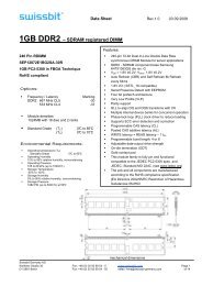
Product data sheet - Swissbit
Product data sheet - Swissbit
Product data sheet - Swissbit

You also want an ePaper? Increase the reach of your titles
YUMPU automatically turns print PDFs into web optimized ePapers that Google loves.
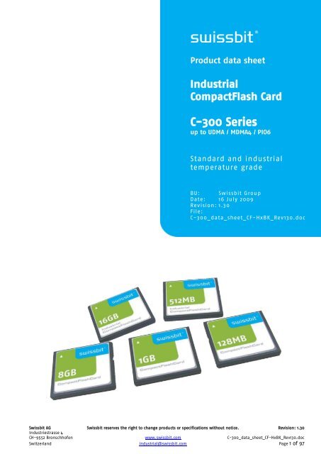
<strong>Product</strong> <strong>data</strong> <strong>sheet</strong><br />
Industrial<br />
CompactFlash Card<br />
C-300 Series<br />
up to UDMA / MDMA4 / PIO6<br />
Standard and industrial<br />
temperature grade<br />
BU: <strong>Swissbit</strong> Group<br />
Date: 16 July 2009<br />
Revision: 1.30<br />
File:<br />
C-300_<strong>data</strong>_<strong>sheet</strong>_CF-HxBK_Rev130.doc<br />
<strong>Swissbit</strong> AG <strong>Swissbit</strong> reserves the right to change products or specifications without notice. Revision: 1.30<br />
Industriestrasse 4<br />
CH-9552 Bronschhofen www.swissbit.com C-300_<strong>data</strong>_<strong>sheet</strong>_CF-HxBK_Rev130.doc<br />
Switzerland industrial@swissbit.com Page 1 of 97
C-300 Series - UDMA CompactFlash Card,<br />
128MByte up to 16GByte, 3.3/5V Supply<br />
1. Features<br />
highly-integrated memory controller<br />
o Fully compliant with CompactFlash TM specification 3.0,<br />
compatible with specification 4.1<br />
o Fully compatible with PCMCIA specification<br />
o PC Card ATA Interface supported<br />
o True IDE mode compatible<br />
o Up to PIO mode 6 supported<br />
o Up to MDMA4 supported<br />
o Up to UDMA4 supported<br />
o Hardware RS-code ECC (4 Bytes/528 Bytes correction)<br />
o Fix drive (IDE mode) &<br />
removable drive (PCMCIA mode) as default in the same card<br />
Small form factor<br />
o CFC Type I: 36.4mm x 42.8mm x 3.3mm<br />
Low-power CMOS technology<br />
3.3V or 5.0V power supply<br />
Power saving mode (with automatic wake-up)<br />
S.M.A.R.T. support optional<br />
Wear Leveling: equal wear leveling of static and dynamic <strong>data</strong><br />
The wear leveling assures that dynamic <strong>data</strong> as well as static <strong>data</strong> is balanced evenly across the<br />
memory. With that the maximum write endurance of the device is guaranteed.<br />
Write Endurance: Due to intelligent wear leveling an even use of the entire flash is guaranteed,<br />
regardless how much “static” (OS) <strong>data</strong> is stored.<br />
Example: If the average file size is 10MByte and the total capacity is 2GByte, 20Mio write cycles can<br />
be performed.<br />
Read Endurance: unlimited<br />
Data Retention: 10 year <strong>data</strong> retention<br />
Patented power-off reliability<br />
o No <strong>data</strong> loss of older sectors<br />
o Max. 16 sectors <strong>data</strong> loss (old <strong>data</strong> kept) if power off 3,00,000 hours<br />
o Data reliability: < 1 non-recoverable error per 10 14 bits read<br />
o Number of connector insertions/removals: >10,000<br />
Hot swappable in PCMCIA modes<br />
High performance<br />
o Up to 66MB/s burst transfer rate in UDMA4<br />
o Sustained Write performance:<br />
up to 20MB/s (UDMA4)<br />
o Sustained Read Performance:<br />
up to 37MB/s (UDMA4)<br />
Available densities<br />
o up to 16GBytes<br />
Operating System support<br />
o Standard Software Drivers operation CompactFlash<br />
Controlled BOM<br />
<strong>Swissbit</strong> AG <strong>Swissbit</strong> reserves the right to change products or specifications without notice. Revision: 1.30<br />
Industriestrasse 4<br />
CH-9552 Bronschhofen www.swissbit.com C-300_<strong>data</strong>_<strong>sheet</strong>_CF-HxBK_Rev130.doc<br />
Switzerland industrial@swissbit.com Page 2 of 97
2. Table of Contents<br />
1. FEATURES........................................................................................................................................................................ 2<br />
2. TABLE OF CONTENTS ........................................................................................................................................................ 3<br />
3. ORDER INFORMATION...................................................................................................................................................... 6<br />
3.1 OFFERED OEM OPTIONS ........................................................................................................................................................... 6<br />
4. PRODUCT SPECIFICATION ................................................................................................................................................. 7<br />
4.1 SYSTEM PERFORMANCE ............................................................................................................................................................ 7<br />
4.2 ENVIRONMENTAL SPECIFICATIONS ............................................................................................................................................... 8<br />
4.3 PHYSICAL DIMENSIONS ........................................................................................................................................................... 9<br />
4.4 RELIABILITY ......................................................................................................................................................................... 9<br />
4.5 DRIVE GEOMETRY / CHS PARAMETER ......................................................................................................................................... 9<br />
4.6 PHYSICAL DESCRIPTION ........................................................................................................................................................... 9<br />
5. ELECTRICAL INTERFACE .................................................................................................................................................. 11<br />
5.1 ELECTRICAL DESCRIPTION ........................................................................................................................................................ 11<br />
5.2 ELECTRICAL SPECIFICATION ..................................................................................................................................................... 18<br />
5.3 ADDITIONAL REQUIREMENTS FOR COMPACTFLASH ADVANCED TIMING MODE ........................................................................................ 19<br />
6. COMMAND INTERFACE ................................................................................................................................................... 20<br />
6.1 ATTRIBUTE MEMORY READ AND WRITE ...................................................................................................................................... 20<br />
6.2 COMMON MEMORY READ AND WRITE ....................................................................................................................................... 21<br />
6.3 I/O READ AND WRITE .......................................................................................................................................................... 23<br />
6.4 TRUE IDE MODE................................................................................................................................................................. 24<br />
6.5 ULTRA DMA MODE ............................................................................................................................................................. 26<br />
7. CARD CONFIGURATION .................................................................................................................................................. 45<br />
7.1 CONFIGURATION OPTION REGISTER (200H IN ATTRIBUTE MEMORY) .................................................................................................. 45<br />
7.2 COMPACTFLASH MEMORY CARD CONFIGURATIONS......................................................................................................................... 46<br />
7.3 PIN REPLACEMENT REGISTER (204H IN ATTRIBUTE MEMORY) ......................................................................................................... 46<br />
7.4 SOCKET AND COPY REGISTER (206H IN ATTRIBUTE MEMORY) ......................................................................................................... 47<br />
7.5 ATTRIBUTE MEMORY FUNCTION ............................................................................................................................................... 47<br />
7.6 I/O TRANSFER FUNCTION ....................................................................................................................................................... 48<br />
7.7 COMMON MEMORY TRANSFER FUNCTION .................................................................................................................................... 48<br />
7.8 TRUE IDE MODE I/O FUNCTION .............................................................................................................................................. 48<br />
7.9 HOST CONFIGURATION REQUIREMENTS FOR MASTER/SLAVE OR NEW TIMING MODES ............................................................................. 49<br />
8. SOFTWARE INTERFACE ................................................................................................................................................... 50<br />
8.1 CF-ATA DRIVE REGISTER SET DEFINITION AND PROTOCOL ............................................................................................................. 50<br />
8.2 MEMORY MAPPED ADDRESSING .............................................................................................................................................. 50<br />
8.3 CONTIGUOUS I/O MAPPED ADDRESSING .................................................................................................................................... 51<br />
8.4 I/O PRIMARY AND SECONDARY ADDRESS CONFIGURATIONS ............................................................................................................ 52<br />
8.5 TRUE IDE MODE ADDRESSING................................................................................................................................................ 52<br />
9. CF-ATA REGISTERS ........................................................................................................................................................ 53<br />
9.1 DATA REGISTER ................................................................................................................................................................... 53<br />
9.2 ERROR REGISTER ................................................................................................................................................................. 53<br />
9.3 FEATURE REGISTER .............................................................................................................................................................. 54<br />
9.4 SECTOR COUNT REGISTER....................................................................................................................................................... 54<br />
9.5 SECTOR NUMBER (LBA 7-0) REGISTER .................................................................................................................................... 54<br />
9.6 CYLINDER LOW (LBA 15-8) REGISTER..................................................................................................................................... 54<br />
9.7 CYLINDER HIGH (LBA 23-16) REGISTER .................................................................................................................................. 54<br />
9.8 DRIVE/HEAD (LBA 27-24) REGISTER ..................................................................................................................................... 54<br />
9.9 STATUS & ALTERNATE STATUS REGISTERS .................................................................................................................................. 55<br />
9.10 DEVICE CONTROL REGISTER................................................................................................................................................... 56<br />
9.11 CARD (DRIVE) ADDRESS REGISTER .......................................................................................................................................... 56<br />
10. CF-ATA COMMAND DESCRIPTION ................................................................................................................................... 58<br />
<strong>Swissbit</strong> AG <strong>Swissbit</strong> reserves the right to change products or specifications without notice. Revision: 1.30<br />
Industriestrasse 4<br />
CH-9552 Bronschhofen www.swissbit.com C-300_<strong>data</strong>_<strong>sheet</strong>_CF-HxBK_Rev130.doc<br />
Switzerland industrial@swissbit.com Page 3 of 97
10.1 CHECK POWER MODE (98H OR E5H) ...................................................................................................................................... 58<br />
10.2 ERASE SECTOR(S) (C0H) ...................................................................................................................................................... 59<br />
10.3 EXECUTE DRIVE DIAGNOSTIC (90H) ........................................................................................................................................ 59<br />
10.4 FLUSH CACHE (E7H) ........................................................................................................................................................... 60<br />
10.5 FORMAT TRACK (50H) ........................................................................................................................................................ 60<br />
10.6 IDENTIFY DEVICE (ECH) ....................................................................................................................................................... 60<br />
10.7 IDLE (97H OR E3H) ............................................................................................................................................................ 68<br />
10.8 IDLE IMMEDIATE (95H OR E1H) ............................................................................................................................................ 68<br />
10.9 INITIALIZE DRIVE PARAMETERS (91H) ..................................................................................................................................... 68<br />
10.10 NOP (00H) ................................................................................................................................................................... 69<br />
10.11 READ BUFFER (E4H) ......................................................................................................................................................... 69<br />
10.12 READ DMA (C8H) ........................................................................................................................................................... 69<br />
10.13 READ MULTIPLE (C4H) ...................................................................................................................................................... 70<br />
10.14 READ SECTOR(S) (20H OR 21H) ........................................................................................................................................... 70<br />
10.15 READ VERIFY SECTOR(S) (40H OR 41H) ................................................................................................................................. 71<br />
10.16 RECALIBRATE (1XH) .......................................................................................................................................................... 71<br />
10.17 REQUEST SENSE (03H) ....................................................................................................................................................... 71<br />
10.18 SEEK (7XH) .................................................................................................................................................................... 72<br />
10.19 SET FEATURES (EFH) ......................................................................................................................................................... 72<br />
10.20 SET MULTIPLE MODE (C6H) ............................................................................................................................................... 74<br />
10.21 SET SLEEP MODE (99H OR E6H).......................................................................................................................................... 75<br />
10.22 S.M.A.R.T. (B0H) ......................................................................................................................................................... 75<br />
10.23 STANDBY (96H OR E2) ..................................................................................................................................................... 76<br />
10.24 STANDBY IMMEDIATE (94H OR E0H) .................................................................................................................................... 76<br />
10.25 TRANSLATE SECTOR (87H) .................................................................................................................................................. 76<br />
10.26 WEAR LEVEL (F5H) .......................................................................................................................................................... 76<br />
10.27 WRITE BUFFER (E8H) ....................................................................................................................................................... 78<br />
10.28 WRITE DMA (CAH) ......................................................................................................................................................... 78<br />
10.29 WRITE MULTIPLE COMMAND (C5H) ...................................................................................................................................... 79<br />
10.30 WRITE MULTIPLE WITHOUT ERASE (CDH) ............................................................................................................................... 79<br />
10.31 WRITE SECTOR(S) (30H OR 31H) .......................................................................................................................................... 80<br />
10.32 WRITE SECTOR(S) WITHOUT ERASE (38H) ............................................................................................................................... 80<br />
10.33 WRITE VERIFY (3CH) ........................................................................................................................................................ 80<br />
11. S.M.A.R.T FUNCTIONALITY ............................................................................................................................................. 81<br />
11.1 S.M.A.R.T. ENABLE / DISABLE OPERATIONS ............................................................................................................................. 81<br />
11.2 S.M.A.R.T. ENABLE / DISABLE ATTRIBUTE AUTOSAVE ................................................................................................................. 81<br />
11.3 S.M.A.R.T. READ DATA ...................................................................................................................................................... 81<br />
11.4 S.M.A.R.T. READ ATTRIBUTE THRESHOLDS .............................................................................................................................. 84<br />
11.5 S.M.A.R.T. RETURN STATUS ................................................................................................................................................ 85<br />
12. CIS INFORMATION (TYPICAL) .......................................................................................................................................... 86<br />
13. PACKAGE MECHANICAL .................................................................................................................................................. 90<br />
14. DECLARATION OF CONFORMITY ...................................................................................................................................... 91<br />
15. ROHS AND WEEE UPDATE FROM SWISSBIT ..................................................................................................................... 92<br />
16. PART NUMBER DECODER ............................................................................................................................................... 94<br />
16.1 MANUFACTURER ................................................................................................................................................................. 94<br />
16.2 MEMORY TYPE .................................................................................................................................................................. 94<br />
16.3 PRODUCT TYPE .................................................................................................................................................................. 94<br />
16.4 DENSITY .......................................................................................................................................................................... 94<br />
16.5 PLATFORM ....................................................................................................................................................................... 94<br />
16.6 PRODUCT GENERATION ........................................................................................................................................................ 94<br />
16.7 MEMORY ORGANIZATION ...................................................................................................................................................... 94<br />
16.8 CONTROLLER TYPE .............................................................................................................................................................. 94<br />
16.9 NUMBER OF FLASH CHIP ..................................................................................................................................................... 94<br />
16.10 FLASH CODE .................................................................................................................................................................... 95<br />
16.11 TEMP. OPTION ................................................................................................................................................................. 95<br />
16.12 DIE CLASSIFICATION .......................................................................................................................................................... 95<br />
16.13 PIN MODE ..................................................................................................................................................................... 95<br />
<strong>Swissbit</strong> AG <strong>Swissbit</strong> reserves the right to change products or specifications without notice. Revision: 1.30<br />
Industriestrasse 4<br />
CH-9552 Bronschhofen www.swissbit.com C-300_<strong>data</strong>_<strong>sheet</strong>_CF-HxBK_Rev130.doc<br />
Switzerland industrial@swissbit.com Page 4 of 97
16.14 COMPACT FLASH XYZ ......................................................................................................................................................... 95<br />
16.15 OPTION .......................................................................................................................................................................... 95<br />
17. SWISSBIT CF LABEL SPECIFICATION ................................................................................................................................ 96<br />
17.1 FRONT SIDE LABEL ............................................................................................................................................................... 96<br />
17.2 BACK SIDE LABEL ................................................................................................................................................................ 96<br />
18. REVISION HISTORY ........................................................................................................................................................ 97<br />
<strong>Swissbit</strong> AG <strong>Swissbit</strong> reserves the right to change products or specifications without notice. Revision: 1.30<br />
Industriestrasse 4<br />
CH-9552 Bronschhofen www.swissbit.com C-300_<strong>data</strong>_<strong>sheet</strong>_CF-HxBK_Rev130.doc<br />
Switzerland industrial@swissbit.com Page 5 of 97
3. Order Information<br />
IDE-FIX & PCMCIA-Removable / PIO, DMA & UDMA support / 0°C – 70°C<br />
Density Part Number<br />
128MB SFCF0128HxBK1SA-C-M0-513-STD<br />
256MB SFCF0256HxBK1SA-C-M0-513-STD<br />
512MB SFCF0512HxBK2SA-C-M0-513-STD<br />
1GB SFCF1024HxBK2SA-C-M0-513-STD<br />
2GB SFCF2048HxBK2SA-C-D0-513-STD<br />
4GB SFCF4096HxBK2SA-C-Q1-513-STD<br />
8GB SFCF8192HxBK4SA-C-Q1-513-STD<br />
16GB SFCF16GBHxBK4SA-C-Q1-513-STD<br />
Table 1: Standard product list<br />
x= depends on product generation<br />
IDE-FIX & PCMCIA-Removable / PIO, DMA & UDMA support / -40°C – +85°C<br />
Density Part Number<br />
128MB SFCF0128HxBK1SA-I-M0-513-STD<br />
256MB SFCF0256HxBK1SA-I-M0-513-STD<br />
512MB SFCF0512HxBK2SA-I-M0-513-STD<br />
1GB SFCF1024HxBK2SA-I-M0-513-STD<br />
2GB SFCF2048HxBK2SA-I-D0-513-STD<br />
4GB SFCF4096HxBK2SA-I-Q1-513-STD<br />
8GB SFCF8192HxBK4SA-I-Q1-513-STD<br />
16GB SFCF16GBHxBK4SA-I-Q1-513-STD<br />
Table 2: Industrial temperature product list<br />
x= depends on product generation<br />
3.1 Offered OEM options<br />
Disabling MDMA and/or UDMA modes<br />
Customer specified card size and card geometry (C/H/S – cylinder/head/sector)<br />
Customer specified CIS and drive ID strings<br />
Preload service (also images with any file system)<br />
Customized front label<br />
2 Temperature ranges<br />
o Commercial Temperature range 0 … +70°C<br />
o Industrial Temperature range -40 … +85°C<br />
ROM mode (write protected with preloaded software)<br />
Adjustments in FW for customer projects<br />
Special Firmware solutions for additional customer requirements<br />
…<br />
<strong>Swissbit</strong> AG <strong>Swissbit</strong> reserves the right to change products or specifications without notice. Revision: 1.30<br />
Industriestrasse 4<br />
CH-9552 Bronschhofen www.swissbit.com C-300_<strong>data</strong>_<strong>sheet</strong>_CF-HxBK_Rev130.doc<br />
Switzerland industrial@swissbit.com Page 6 of 97
4. <strong>Product</strong> Specification<br />
The CompactFlash is a small form factor non-volatile memory card which provides high capacity <strong>data</strong> storage. Its<br />
aim is to capture, retain and transport <strong>data</strong>, audio and images, facilitating the transfer of all types of digital<br />
information between a large variety of digital systems.<br />
The Card operates in three basic modes:<br />
PC card ATA I/O mode<br />
PC card ATA memory mode<br />
True IDE mode<br />
The CompactFlash also supports Advanced Timing modes. Advanced Timing modes are ATA I/O modes that are<br />
100ns or faster, ATA Memory modes that are 100ns or 80ns.<br />
Standard cards are shipped as max. PIO6 and MDMA4 (80ns) and UDMA4 (30ns).<br />
If the cards should be used in extended speed modes, they should be qualified on the target system and the<br />
system should fulfill the requirements listed below.<br />
It conforms to the PCMCIA Card Specification 2.1 when operating in the ATA I/O mode, and in the ATA Memory mode<br />
(Personal Computer Memory Card International Association standard, JEIDA in Japan), and to the ATA specification<br />
when operating in True IDE Mode. CompactFlash Cards can be used with passive adapters in a PC-Card Type II or<br />
Type III socket.<br />
The Card has an internal intelligent controller which manages interface protocols, <strong>data</strong> storage and retrieval as<br />
well as hardware RS-code Error Correction Code (ECC), defect handling, diagnostics and clock control.<br />
The wear leveling mechanism assures an equal usage of the Flash memory cells to extend the life time.<br />
Once the Card has been configured by the host, it behaves as a standard ATA (IDE) disk drive. The hardware RScode<br />
ECC allows to detect and correct 4 symbols per 528 Bytes.<br />
The Card has a voltage detector and a powerful power-loss management feature to prevent <strong>data</strong> corruption after<br />
power-down.<br />
The specification has been realized and approved by the CompactFlash Association (CFA).<br />
This non-proprietary specification enables users to develop CF products that function correctly and are compatible<br />
with future CF design. The system highlights are shown in Table 3 … Table 9.<br />
Related Documentation<br />
PCMCIA PC Card Standard, 1995<br />
PCMCIA PC Card ATA Specification, 1995<br />
AT Attachment Interface Document, American National Standards Institute, X3.221-1994<br />
CF+ and CompactFlash Specification Revision 3.0<br />
4.1 System Performance<br />
Table 3: System Performance<br />
System Performance Typ. Max. Unit<br />
Sleep to write 5<br />
Sleep to read<br />
Power up to Ready
Requirements for using extended speed (PIO 5, 6/ MDMA 3, 4)<br />
(CompactFlash Specification 3.0; section 4.3.7)<br />
The CF Advanced Timing modes include PCMCIA I/O and Memory modes that are 100ns or faster and True<br />
IDE PIO Modes 5,6 and Multiword DMA Modes 3,4.<br />
When operating in CF Advanced timing modes, the host shall conform to the following requirements:<br />
1. Only one CF device shall be attached to the CF Bus.<br />
2. The host shall not present a load of more than 40pF to the device for all signals, including any cabling.<br />
3. The maximum cable length is 0.05 m (2 in). The cable length is measured from the card connector to the<br />
host controller. 0.46 m (18 in) cables are not supported.<br />
4. The –WAIT and IORDY signals shall be ignored by the host.<br />
Devices supporting CF Advanced timing modes shall also support slower timing modes, to ensure operability with<br />
systems that do not support CF Advanced timing modes.<br />
Ultra DMA Electrical Requirements<br />
(CompactFlash Specification 3.0; section 4.3.8)<br />
Operation in Ultra DMA mode requires careful attention to cabling, printed circuit board (PCB) trace routing and<br />
termination for reliable operation. These requirements are described in the following sections.<br />
Host and Card signal capacitance limits for Ultra DMA operation<br />
The host interface signal capacitance at the host connector shall be a maximum of 25pF for each signal as<br />
measured at 1 MHz.<br />
The card interface signal capacitance at the card connector shall be a maximum of 20pF for each signal as<br />
measured at 1 MHz.<br />
Series termination required for Ultra DMA operation<br />
Series termination resistors are required at both the host and the card for operation in any of the Ultra DMA<br />
modes. The CF specification describes typical values for series termination at the host and the device.<br />
4.2 Environmental Specifications<br />
4.2.1 Recommended Operating Conditions<br />
Table 4: CF Card Recommended Operating Conditions<br />
Parameter Value<br />
Commercial Operating Temperature 0°C to 70°C<br />
Industrial Operating Temperature -40°C to 85°C<br />
Power Supply VCC Voltage (5V) 4.5V to 5.5V – 5.0V ±10%<br />
Power Supply VCC Voltage (3.3V) 2.97V to 3.63V – 3.3V ±10%<br />
Table 5: Current consumption (1)<br />
Current Consumption (type) 3.3V 5V Unit<br />
Read (MDMA2/UDMA4/max) 60 / 80 / 130 85 / 120 / 140<br />
Write (MDMA2/UDMA4/max) 60 / 80 / 120 95 / 110 / 130<br />
mA<br />
Sleep/Idle Mode (typ/max) 0.5 / 1.5 1.5 / 2.0<br />
1. All values are typical at 25° C and nominal supply voltage and refer to 1Gbyte CompactFlash Card.<br />
Max values are for 8GB cards in UDMA4 mode in IDE mode.<br />
The card goes to Sleep/idle mode 20ms (default) after last host command.<br />
4.2.2 Recommended Storage Conditions<br />
Table 6: CF Card Recommended Storage Conditions<br />
Parameter Value<br />
Commercial Storage Temperature -65°C to 150°C<br />
Industrial Storage Temperature -65°C to 150°C<br />
<strong>Swissbit</strong> AG <strong>Swissbit</strong> reserves the right to change products or specifications without notice. Revision: 1.30<br />
Industriestrasse 4<br />
CH-9552 Bronschhofen www.swissbit.com C-300_<strong>data</strong>_<strong>sheet</strong>_CF-HxBK_Rev130.doc<br />
Switzerland industrial@swissbit.com Page 8 of 97
4.2.3 Shock, Vibration, and Humidity<br />
Table 7: Shock, Vibration, and Humidity<br />
Parameter Value<br />
Humidity (non-condensing) 85% RH 85°C, 1000 hrs (JEDEC JESD22, method A101-B)<br />
Vibration 20 G peak, 20-2000Hz, 4 per direction (JEDEC JESD22, method B103)<br />
5.35G RMS, 15 min per plane (IEC 68-2-6)<br />
Shock 1.5k G peak, 0.5ms 5 times (JEDEC JESD22, method B110)<br />
30 G, 11ms 1 time (IEC 68-2-27)<br />
4.3 Physical Dimensions<br />
Table 8: Physical Dimensions<br />
Parameter Value Unit<br />
Width 42.8<br />
Height 36.4<br />
mm<br />
Thickness 3.3<br />
Weight (typ.) 10 g<br />
4.4 Reliability<br />
Table 9: System Reliability and Maintenance<br />
Parameter Value<br />
MTBF (at 25°C) > 3,000,000 hours<br />
Insertions/Removals > 10,000<br />
Data Reliability < 1 Non-Recoverable Error per 10 14 bits Read<br />
Data Retention 10 years<br />
23. . . . Dependent on final system qualification <strong>data</strong>.<br />
4.5 Drive Geometry / CHS Parameter<br />
Table 10: CF capacity specification<br />
Capacity Cylinders Heads Sectors / track Sectors Total addressable capacity (Byte)<br />
32MB 496 4 32 63,488 32,505,856<br />
64MB 490 8 32 125,440 64,225,280<br />
128MB 980 8 32 250,880 128,450,560<br />
256MB 980 16 32 501,760 256,901,120<br />
512MB 993 16 63 1,000,944 512,483,328<br />
1GB 1,986 16 63 2,001,888 1,024,966,656<br />
2GB 3,970 16 63 4,001,760 2,048,901,120<br />
4GB 7,964 16 63 8,027,712 4,110,188,544<br />
8GB 15,880 16 63 16,007,040 8,195,604,480<br />
16GB 16,383 (1) 16 63 31,717,728 16,239,476,736<br />
(1) The CHS addressing is limited to about 8GB. Larger drives should be used in LBA mode.<br />
4.6 Physical description<br />
The CompactFlash Memory Card contains a single chip controller and Flash memory module(s). The controller<br />
interfaces with a host system allowing <strong>data</strong> to be written to and read from the Flash memory module(s). Figure 1<br />
shows the Block Diagram of the CompactFlash Memory Card.<br />
The Card is offered in a Type I package with a 50-pin connector consisting of two rows of 25 female contacts on 50<br />
mil (1.27mm) centers. Figure 21 shows Type I Card Dimensions.<br />
<strong>Swissbit</strong> AG <strong>Swissbit</strong> reserves the right to change products or specifications without notice. Revision: 1.30<br />
Industriestrasse 4<br />
CH-9552 Bronschhofen www.swissbit.com C-300_<strong>data</strong>_<strong>sheet</strong>_CF-HxBK_Rev130.doc<br />
Switzerland industrial@swissbit.com Page 9 of 97
Figure 1: CompactFlash Memory Card Block Diagram<br />
<strong>Swissbit</strong> AG <strong>Swissbit</strong> reserves the right to change products or specifications without notice. Revision: 1.30<br />
Industriestrasse 4<br />
CH-9552 Bronschhofen www.swissbit.com C-300_<strong>data</strong>_<strong>sheet</strong>_CF-HxBK_Rev130.doc<br />
Switzerland industrial@swissbit.com Page 10 of 97
5. Electrical interface<br />
5.1 Electrical description<br />
The CompactFlash Memory Card operates in three basic modes:<br />
PC Card ATA using I/O Mode<br />
PC Card ATA using Memory Mode<br />
True IDE Mode with MWDMA and UDMA, which is compatible with most disk drives<br />
The signal/pin assignments are listed in Table 11 Low active signals have a ‘-’ prefix. Pin types are Input, Output or<br />
Input/Output.<br />
The configuration of the Card is controlled using the standard PCMCIA configuration registers starting at address<br />
200h in the Attribute Memory space of the memory card.<br />
<strong>Swissbit</strong> AG <strong>Swissbit</strong> reserves the right to change products or specifications without notice. Revision: 1.30<br />
Industriestrasse 4<br />
CH-9552 Bronschhofen www.swissbit.com C-300_<strong>data</strong>_<strong>sheet</strong>_CF-HxBK_Rev130.doc<br />
Switzerland industrial@swissbit.com Page 11 of 97
Table 12 describes the I/O signals. Inputs are signals sourced from the host while Outputs are signals sourced from<br />
the Card. The signals are described for each of the three operating modes.<br />
All outputs from the Card are totem pole except the <strong>data</strong> bus signals that are bi-directional tri-state. Refer to the<br />
section titled “Electrical Specifications” for definitions of Input and Output type.<br />
Table 11: Pin Assignment and Pin Type<br />
Pin Num PC Card Memory Mode PC Card I/O Mode True IDE Mode (4)<br />
Signal Pin In, Out Signal Pin In, Out Signal Pin In, Out<br />
Name Type Type Name Type Type Name Type Type<br />
1 GND Ground GND Ground GND Ground<br />
2 D03 I/O I1Z,OZ3 D03 I/O I1Z,OZ3 D03 I/O I1Z,OZ3<br />
3 D04 I/O I1Z,OZ3 D04 I/O I1Z,OZ3 D04 I/O I1Z,OZ3<br />
4 D05 I/O I1Z,OZ3 D05 I/O I1Z,OZ3 D05 I/O I1Z,OZ3<br />
5 D06 I/O I1Z,OZ3 D06 I/O I1Z,OZ3 D06 I/O I1Z,OZ3<br />
6 D07 I/O I1Z,OZ3 D07 I/O I1Z,OZ3 D07 I/O I1Z,OZ3<br />
7 -CE1 I I3U -CE1 I I3U -CS0 I I3Z<br />
8 A10 I I1Z A10 I I1Z A10 (2) I I1Z<br />
9 (1) -OE I I3U -OE I I3U -ATASEL I I3U<br />
10 A09 I I1Z A09 I I1Z A09 (2) I I1Z<br />
11 A08 I I1Z A08 I I1Z A08 (2) I I1Z<br />
12 A07 I I1Z A07 I I1Z A07 (2) I I1Z<br />
13 Vcc Power Vcc Power Vcc Power<br />
14 A06 I I1Z A06 I I1Z A06 (2) I I1Z<br />
15 A05 I I1Z A05 I I1Z A05 (2) I I1Z<br />
16 A04 I I1Z A04 I I1Z A04 (2) I I1Z<br />
17 A03 I I1Z A03 I I1Z A03 (2) I I1Z<br />
18 A02 I I1Z A02 I I1Z A02 I I1Z<br />
19 A01 I I1Z A01 I I1Z A01 I I1Z<br />
20 A00 I I1Z A00 I I1Z A00 I I1Z<br />
21 D00 I/O I1Z,OZ3 D00 I/O I1Z,OZ3 D00 I/O I1Z,OZ3<br />
22 D01 I/O I1Z,OZ3 D01 I/O I1Z,OZ3 D01 I/O I1Z,OZ3<br />
23 D02 I/O I1Z,OZ3 D02 I/O I1Z,OZ3 D02 I/O I1Z,OZ3<br />
24 WP O OT3 -IOIS16 O OT3 -IOIS16 O ON3<br />
25 -CD2 O Ground -CD2 O Ground -CD2 O Ground<br />
26 -CD1 O Ground -CD1 O Ground -CD1 O Ground<br />
27 D11 (1) I/O I1Z,OZ3 D11 (1) I/O I1Z,OZ3 D11 (1) I/O I1Z,OZ3<br />
28 D12 (1) I/O I1Z,OZ3 D12 (1) I/O I1Z,OZ3 D12 (1) I/O I1Z,OZ3<br />
29 D13 (1) I/O I1Z,OZ3 D13 (1) I/O I1Z,OZ3 D13 (1) I/O I1Z,OZ3<br />
30 D14 (1) I/O I1Z,OZ3 D14 (1) I/O I1Z,OZ3 D14 (1) I/O I1Z,OZ3<br />
31 D15 (1) I/O I1Z,OZ3 D15 (1) I/O I1Z,OZ3 D15 (1) I/O I1Z,OZ3<br />
32 -CE2 (1)<br />
I I3U -CE2 (1)<br />
I I3U -CS1 (1)<br />
I I3Z<br />
33 -VS1 O Ground -VS1 O Ground -VS1<br />
-IORD<br />
O Ground<br />
34 -IORD I I3U -IORD I I3U<br />
(7)<br />
HSTROBE I I3Z<br />
(8)<br />
-HDMARDY (9)<br />
35 -IOWR I I3U -IOWR I I3U<br />
-IOWR (7)<br />
STOP (8)(9)<br />
36 -WE I I3U -WE I I3U -WE (3)<br />
I I3Z<br />
I I3U<br />
37 READY O OT1 -IREQ O OT1 INTRQ O OZ1<br />
38 Vcc Power Vcc Power Vcc Power<br />
39 -CSEL (5)<br />
I I2Z -CSEL (5)<br />
I I2Z -CSEL<br />
I I2U<br />
<strong>Swissbit</strong> AG <strong>Swissbit</strong> reserves the right to change products or specifications without notice. Revision: 1.30<br />
Industriestrasse 4<br />
CH-9552 Bronschhofen www.swissbit.com C-300_<strong>data</strong>_<strong>sheet</strong>_CF-HxBK_Rev130.doc<br />
Switzerland industrial@swissbit.com Page 12 of 97
Pin Num PC Card Memory Mode PC Card I/O Mode True IDE Mode (4)<br />
Signal<br />
Name<br />
Pin<br />
Type<br />
In, Out<br />
Type<br />
Signal<br />
Name<br />
Pin<br />
Type<br />
In, Out<br />
Type<br />
Signal<br />
Name<br />
<strong>Swissbit</strong> AG <strong>Swissbit</strong> reserves the right to change products or specifications without notice. Revision: 1.30<br />
Industriestrasse 4<br />
CH-9552 Bronschhofen www.swissbit.com C-300_<strong>data</strong>_<strong>sheet</strong>_CF-HxBK_Rev130.doc<br />
Switzerland industrial@swissbit.com Page 13 of 97<br />
Pin<br />
Type<br />
In, Out<br />
Type<br />
40 -VS2 O OPEN -VS2 O OPEN -VS2 O OPEN<br />
41 RESET I I2Z RESET I I2Z -RESET<br />
IORDY<br />
I I2Z<br />
42 -WAIT O OT1 -WAIT O OT1<br />
(7)<br />
O ON1<br />
-DDMARDY (8)<br />
DSTROBE (9)<br />
43 -INPACK O OT1 -INPACK O OT1 DMARQ O OZ1<br />
44 -REG I I3U -REG I I3U -DMACK (6) I I3U<br />
45 BVD2 I/O I1U,OT1 -SPKR I/O I1U,OT1 -DASP I/O I1U,ON1<br />
46 BVD1 I/O I1U,OT1 -STSCHG I/O I1U,OT1 -PDIAG I/O I1U,ON1<br />
47 D08 (1) I/O I1Z,OZ3 D08 (1) I/O I1Z,OZ3 D08 (1) I/O I1Z,OZ3<br />
48 D09 (1) I/O I1Z,OZ3 D09 (1) I/O I1Z,OZ3 D09 (1) I/O I1Z,OZ3<br />
49 D10 (1) I/O I1Z,OZ3 D10 (1) I/O I1Z,OZ3 D10 (1) I/O I1Z,OZ3<br />
50 GND Ground GND Ground GND Ground<br />
1. These signals are required only for 16 bit accesses and not required when installed in 8 bit systems.<br />
Devices should allow for 3-state signals not to consume current.<br />
2. The signal should be grounded by the host.<br />
3. The signal should be tied to VCC by the host.<br />
4. The mode is optional for CF+ Cards, but required for CompactFlash Storage Cards.<br />
5. The –CSEL signal is ignored by the card in PC Card modes. However, because it is not pulled up on the card<br />
in these modes, it should not be left floating by the host in PC Card modes. In these modes, the pin<br />
should be connected by the host to PC Card A25 or grounded by the host.<br />
6. If DMA operations are not used, the signal should be held high or tied to VCC by the host. For proper<br />
operation in older hosts: while DMA operations are not active, the card shall ignore this signal, including<br />
a floating condition<br />
7. Signal usage in True IDE Mode except when Ultra DMA mode protocol is active.<br />
8. Signal usage in True IDE Mode when Ultra DMA mode protocol DMA Write is active.<br />
9. Signal usage in True IDE Mode when Ultra DMA mode protocol DMA Read is active. The signal should be<br />
grounded by the host.
Table 12: Signal Description<br />
Signal Name Dir. Pin Description<br />
These address lines along with the –REG signal are used to<br />
select the following: The I/O port address registers within the<br />
A10 to A0<br />
CompactFlash Storage Card or CF+ Card, the memory mapped<br />
(PC Card Memory Mode)<br />
port address registers within the CompactFlash Storage Card or<br />
I<br />
8,10,11,12, CF+ Card, a byte in the card’s information structure and its<br />
14,15,16,17, configuration control and status registers.<br />
A10 to A0<br />
(PC Card I/O Mode)<br />
18,19,20<br />
This signal is the same as the PC Card Memory Mode signal.<br />
A2 to A0<br />
(True IDE Mode)<br />
In True IDE Mode, only A[2:0] are used to select the one of eight<br />
registers in the Task File, the remaining address lines should be<br />
grounded by the host.<br />
BVD1<br />
(PC Card Memory Mode)<br />
This signal is asserted high, as BVD1 is not supported.<br />
This signal is asserted low to alert the host to changes in the<br />
–STSCHG<br />
(PC Card I/O Mode)<br />
I/O 46<br />
READY and Write Protect states, while the I/O interface is<br />
configured. Its use is controlled by the Card Config and Status<br />
Register.<br />
–PDIAG<br />
In the True IDE Mode, this input / output is the Pass Diagnostic<br />
(True IDE Mode)<br />
signal in the Master / Slave handshake protocol.<br />
BVD2<br />
(PC Card Memory Mode)<br />
This signal is asserted high, as BVD2 is not supported.<br />
–SPKR<br />
(PC Card I/O Mode)<br />
I/O 45<br />
This line is the Binary Audio output from the card. If the Card<br />
does not support the Binary Audio function, this line should be<br />
held negated.<br />
–DASP<br />
In the True IDE Mode, this input/output is the Disk Active/Slave<br />
(True IDE Mode)<br />
Present signal in the Master/Slave handshake protocol.<br />
These lines carry the Data, Commands and Status information<br />
D15-D00 (PC Card Memory Mode) 31, 30, 29, between the host and the controller. D00 is the LSB of the Even<br />
28, 27, 49, Byte of the Word. D08 is the LSB of the Odd Byte of the Word.<br />
D15-D00 (PC Card I/O Mode) I/O 48, 47, 6, This signal is the same as the PC Card Memory Mode signal.<br />
5, 4, 3, 2, In True IDE Mode, all Task File operations occur in byte mode<br />
D15-D00 (True IDE Mode)<br />
23, 22, 21 on the low order bus D[7:0] while all <strong>data</strong> transfers are 16 bit<br />
using D[15:0].<br />
GND<br />
(PC Card Memory Mode)<br />
Ground.<br />
GND<br />
(PC Card I/O Mode)<br />
1, 50 Same for all modes.<br />
GND<br />
(True IDE Mode)<br />
Same for all modes.<br />
–INPACK<br />
(PC Card Memory Mode)<br />
This signal is not used in this mode.<br />
The Input Acknowledge signal is asserted by the CompactFlash<br />
Storage Card or CF+ Card when the card is selected and<br />
–INPACK<br />
(PC Card I/O Mode)<br />
O 43 responding to an I/O read cycle at the address that is on the<br />
address bus. This signal is used by the host to control the<br />
enable<br />
of any input <strong>data</strong> buffers between the CompactFlash Storage<br />
Card or CF+ Card and the CPU.<br />
<strong>Swissbit</strong> AG <strong>Swissbit</strong> reserves the right to change products or specifications without notice. Revision: 1.30<br />
Industriestrasse 4<br />
CH-9552 Bronschhofen www.swissbit.com C-300_<strong>data</strong>_<strong>sheet</strong>_CF-HxBK_Rev130.doc<br />
Switzerland industrial@swissbit.com Page 14 of 97
DMARQ<br />
(True IDE Mode)<br />
Signal Name Dir. Pin Description<br />
–IORD<br />
(PC Card Memory Mode)<br />
–IORD<br />
(PC Card I/O Mode)<br />
–IORD<br />
(True IDE Mode)<br />
-HDMARDY<br />
(True IDE Mode – In Ultra<br />
DMA Protocol DMA<br />
Read)<br />
HSTROBE<br />
(True IDE Mode – In Ultra<br />
DMA Protocol DMA<br />
Write)<br />
–CD1, –CD2<br />
(PC Card Memory Mode)<br />
–CD1, –CD2<br />
(PC Card I/O Mode)<br />
–CD1, –CD2<br />
(True IDE Mode)<br />
–CE1, –CE2<br />
(PC Card Memory Mode)<br />
–CE1, –CE2<br />
(PC Card I/O Mode)<br />
–CS0, –CS1<br />
(True IDE Mode)<br />
–CSEL<br />
(PC Card Memory Mode)<br />
I 34<br />
O 26, 25<br />
I 7, 32<br />
I 39<br />
This signal is a DMA Request that is used for DMA <strong>data</strong><br />
transfers between host and device. It shall be asserted by the<br />
device when it is ready to transfer <strong>data</strong> to or from the host. For<br />
Multiword DMA transfers, the direction of <strong>data</strong> transfer is<br />
controlled by –IORD and –IOWR. This signal is used in a<br />
handshake manner with –DMACK, i.e., the device shall wait<br />
until<br />
the host asserts –DMACK before negating DMARQ, and<br />
reasserting<br />
DMARQ if there is more <strong>data</strong> to transfer.<br />
DMARQ shall not be driven when the device is not selected.<br />
While a DMA operation is in progress, -CS0 and –CS1 shall be<br />
held negated and the width of the transfers shall be 16 bits.<br />
If there is no hardware support for DMA mode in the host, this<br />
output signal is not used and should not be connected at the<br />
host. In this case, the BIOS must report that DMA mode is not<br />
supported by the host so that device drivers will not attempt<br />
DMA<br />
mode.<br />
A host that does not support DMA mode and implements both<br />
PCMCIA and True-IDE modes of operation need not alter the<br />
PCMCIA mode connections while in True-IDE mode as long as<br />
this does not prevent proper operation in any mode.<br />
This signal is not used in this mode.<br />
This is an I/O Read strobe generated by the host. This signal<br />
gates I/O <strong>data</strong> onto the bus from the CompactFlash Storage<br />
Card or CF+ Card when the card is configured to use the I/O<br />
interface.<br />
In True IDE Mode, while Ultra DMA mode is not active, this<br />
signal has the same function as in PC Card I/O Mode.<br />
In True IDE Mode when Ultra DMA mode DMA Read is active,<br />
this signal is asserted by the host to indicate that the host is<br />
read<br />
to receive Ultra DMA <strong>data</strong>-in bursts. The host may negate<br />
-HDMARDY to pause an Ultra DMA transfer.<br />
In True IDE Mode when Ultra DMA mode DMA Write is active,<br />
this signal is the <strong>data</strong> out strobe generated by the host. Both<br />
the<br />
rising and falling edge of HSTROBE cause <strong>data</strong> to be latched by<br />
the device. The host may stop generating HSTROBE edges to<br />
pause an Ultra DMA <strong>data</strong>-out burst.<br />
These Card Detect pins are connected to ground on the<br />
CompactFlash Storage Card or CF+ Card. They are used by the<br />
host to determine that the CompactFlash Storage Card or CF+<br />
Card is fully inserted into its socket.<br />
This signal is the same for all modes.<br />
This signal is the same for all modes.<br />
These input signals are used both to select the card and to<br />
indicate to the card whether a byte or a word operation is being<br />
performed. –CE2 always accesses the odd byte of the word.<br />
-CE1 accesses the even byte or the Odd byte of the word<br />
depending on A0 and –CE2. A multiplexing scheme based on<br />
A0,<br />
-CE1, -CE2 allows 8 bit hosts to access all <strong>data</strong> on D0-D7. See<br />
Table 32, Table 40, Table 41Table 42, and Table 43.<br />
This signal is the same as the PC Card Memory Mode signal.<br />
In the True IDE Mode, -CS0 is the chip select for the task file<br />
registers while –CS1 is used to select the Alternate Status<br />
Register and the Device Control Register.<br />
While –DMACK is asserted, -CS0 and –CS1 shall be held<br />
negated and the width of the transfers shall be 16 bits.<br />
This signal is not used for this mode, but should be connected<br />
by<br />
the host to PC Card A25 or grounded by the host.<br />
<strong>Swissbit</strong> AG <strong>Swissbit</strong> reserves the right to change products or specifications without notice. Revision: 1.30<br />
Industriestrasse 4<br />
CH-9552 Bronschhofen www.swissbit.com C-300_<strong>data</strong>_<strong>sheet</strong>_CF-HxBK_Rev130.doc<br />
Switzerland industrial@swissbit.com Page 15 of 97
–CSEL<br />
(PC Card I/O Mode)<br />
–CSEL<br />
(True IDE Mode)<br />
Signal Name Dir. Pin Description<br />
–IOWR<br />
(PC Card Memory Mode)<br />
–IOWR<br />
(PC Card I/O Mode)<br />
-IOWR<br />
(True IDE Mode – Except<br />
Ultra DMA Protocol<br />
Active)<br />
STOP<br />
(True IDE Mode – Ultra<br />
DMA Protocol Active)<br />
–OE<br />
(PC Card Memory Mode)<br />
–OE<br />
(PC Card I/O Mode)<br />
–ATASEL<br />
(True IDE Mode)<br />
READY<br />
(PC Card Memory Mode)<br />
–IREQ<br />
(PC Card I/O Mode)<br />
INTRQ<br />
(True IDE Mode)<br />
–REG<br />
(PC Card Memory Mode)<br />
–REG<br />
(PC Card I/O Mode)<br />
–DMACK<br />
(True IDE Mode)<br />
I 35<br />
I 9<br />
O 37<br />
I 44<br />
This signal is not used for this mode, but should be connected<br />
by<br />
the host to PC Card A25 or grounded by the host.<br />
This internally pulled up signal is used to configure this device<br />
as<br />
a Master or a Slave when configured in the True IDE Mode.<br />
When this pin is grounded, this device is configured as a<br />
Master.<br />
When the pin is open, this device is configured as a Slave.<br />
This signal is not used in this mode.<br />
The I/O Write strobe pulse is used to clock I/O <strong>data</strong> on the Card<br />
Data bus into the CompactFlash Storage Card or CF+ Card<br />
controller registers when the CompactFlash Storage Card or<br />
CF+ Card is configured to use the I/O interface.<br />
The clocking shall occur on the negative to positive edge of the<br />
signal (trailing edge).<br />
In True IDE Mode, while Ultra DMA mode protocol is not active,<br />
this signal has the same function as in PC Card I/O Mode.<br />
When Ultra DMA mode protocol is supported, this signal must be<br />
negated before entering Ultra DMA mode protocol.<br />
In True IDE Mode, while Ultra DMA mode protocol is active, the<br />
assertion of this signal causes the termination of the Ultra DMA<br />
burst.<br />
This is an Output Enable strobe generated by the host interface.<br />
It is used to read <strong>data</strong> from the CompactFlash Storage Card or<br />
CF+ Card in Memory Mode and to read the CIS and<br />
configuration registers.<br />
In PC Card I/O Mode, this signal is used to read the CIS and<br />
configuration registers.<br />
To enable True IDE Mode this input should be grounded by the<br />
host.<br />
In Memory Mode, this signal is set high when the CompactFlash<br />
Storage Card or CF+ Card is ready to accept a new <strong>data</strong> transfer<br />
operation and is held low when the card is busy.<br />
At power up and at Reset, the READY signal is held low (busy)<br />
until the CompactFlash Storage Card or CF+ Card has<br />
completed its power up or reset function. No access of any type<br />
should be made to the CompactFlash Storage Card or CF+ Card<br />
during this time.<br />
Note, however, that when a card is powered up and used with<br />
RESET continuously disconnected or asserted, the Reset<br />
function of the RESET pin is disabled. Consequently, the<br />
continuous assertion of RESET from the application of power<br />
shall not cause the READY signal to remain continuously in the<br />
busy state.<br />
I/O Operation – After the CompactFlash Storage Card or CF+<br />
Card has been configured for I/O operation, this signal is used as<br />
-Interrupt Request. This line is strobed low to generate a pulse<br />
mode interrupt or held low for a level mode interrupt.<br />
In True IDE Mode signal is the active high Interrupt Request to<br />
the host.<br />
This signal is used during Memory Cycles to distinguish between<br />
Common Memory and Register (Attribute) Memory accesses.<br />
High for Common Memory, Low for Attribute Memory.<br />
The signal shall also be active (low) during I/O Cycles when the<br />
I/O address is on the Bus.<br />
This is a DMA Acknowledge signal that is asserted by the host in<br />
response to DMARQ to initiate DMA transfers.<br />
While DMA operations are not active, the card shall ignore the<br />
-DMACK signal, including a floating condition.<br />
If DMA operation is not supported by a True IDE Mode only host,<br />
this signal should be driven high or connected to VCC by the<br />
host.<br />
A host that does not support DMA mode and implements both<br />
PCMCIA and True-IDE modes of operation need not alter the<br />
PCMCIA mode connections while in True-IDE mode as long as<br />
this does not prevent proper operation all modes.<br />
<strong>Swissbit</strong> AG <strong>Swissbit</strong> reserves the right to change products or specifications without notice. Revision: 1.30<br />
Industriestrasse 4<br />
CH-9552 Bronschhofen www.swissbit.com C-300_<strong>data</strong>_<strong>sheet</strong>_CF-HxBK_Rev130.doc<br />
Switzerland industrial@swissbit.com Page 16 of 97
Signal Name Dir. Pin Description<br />
RESET<br />
(PC Card Memory Mode)<br />
RESET<br />
(PC Card I/O Mode)<br />
–RESET<br />
(True IDE Mode)<br />
Vcc<br />
(PC Card Memory Mode)<br />
Vcc<br />
(PC Card I/O Mode)<br />
Vcc<br />
(True IDE Mode)<br />
–VS1, –VS2<br />
(PC Card Memory Mode)<br />
–VS1, –VS2<br />
(PC Card I/O Mode)<br />
–VS1, –VS2<br />
(True IDE Mode)<br />
–WAIT<br />
(PC Card Memory Mode)<br />
–WAIT<br />
(PC Card I/O Mode)<br />
IORDY<br />
(True IDE Mode – Except<br />
Ultra DMA Mode)<br />
-DDMARDY<br />
(True IDE Mode – Ultra<br />
DMA Write Mode)<br />
DSTROBE<br />
(True IDE Mode – Ultra<br />
DMA Read Mode)<br />
–WE<br />
(PC Card Memory Mode)<br />
–WE<br />
(PC Card I/O Mode)<br />
–WE<br />
(True IDE Mode)<br />
WP<br />
(PC Card Memory Mode)<br />
–IOIS16<br />
(PC Card I/O Mode)<br />
–IOCS16<br />
(True IDE Mode)<br />
I 41<br />
13, 38<br />
O 33, 40<br />
O 42<br />
I 36<br />
O 24<br />
The CompactFlash Storage Card or CF+ Card is Reset when the<br />
RESET pin is high with the following important exception:<br />
The host may leave the RESET pin open or keep it continually<br />
high from the application of power without causing a<br />
continuous<br />
Reset of the card. Under either of these conditions, the card<br />
shall emerge from power-up having completed an initial Reset.<br />
The CompactFlash Storage Card or CF+ Card is also Reset<br />
when the Soft Reset bit in the Card Configuration Option<br />
Register is set.<br />
This signal is the same as the PC Card Memory Mode signal.<br />
In the True IDE Mode, this input pin is the active low hardware<br />
reset from the host.<br />
+5V, +3.3V power.<br />
Same for all modes.<br />
Same for all modes.<br />
Voltage Sense Signals. –VS1 is grounded on the Card and<br />
sensed by the Host so that the CompactFlash Storage Card or<br />
CF+ Card CIS can be read at 3.3 volts and –VS2 is reserved by<br />
PCMCIA for a secondary voltage and is not connected on the<br />
Card.<br />
This signal is the same for all modes.<br />
This signal is the same for all modes.<br />
The –WAIT signal is driven low by the CompactFlash Storage<br />
Card or CF+ Card to signal the host to delay completion of a<br />
memory or I/O cycle that is in progress.<br />
This signal is the same as the PC Card Memory Mode signal.<br />
In True IDE Mode, except in Ultra DMA modes, this output<br />
signal may be used as IORDY.<br />
In True IDE Mode, when Ultra DMA mode DMA Write is active,<br />
this signal is asserted by the host to indicate that the device is<br />
read to receive Ultra DMA <strong>data</strong>-in bursts. The device may<br />
negate –DDMARDY to pause an Ultra DMA transfer.<br />
In True IDE Mode, when Ultra DMA mode DMA Write is active,<br />
this signal is the <strong>data</strong> out strobe generated by the device. Both<br />
the rising and falling edge of DSTROBE cause <strong>data</strong> to be latched<br />
by the host. The device may stop generating DSTROBE edges<br />
to pause an Ultra DMA <strong>data</strong>-out burst.<br />
This is a signal driven by the host and used for strobing memory<br />
write <strong>data</strong> to the registers of the CompactFlash Storage Card or<br />
CF+ Card when the card is configured in the memory interface<br />
mode. It is also used for writing the configuration registers.<br />
In PC Card I/O Mode, this signal is used for writing the<br />
configuration registers.<br />
In True IDE Mode, this input signal is not used and should be<br />
connected to VCC by the host.<br />
Memory Mode – The CompactFlash Storage Card or CF+ Card<br />
does not have a write protect switch. This signal is held low<br />
after<br />
the completion of the reset initialization sequence.<br />
I/O Operation – When the CompactFlash Storage Card or CF+<br />
Card is configured for I/O Operation Pin 24 is used for the –I/O<br />
Selected is 16 Bit Port (-IOIS16) function. A Low signal indicates<br />
that a 16 bit or odd byte only operation can be performed at the<br />
addressed port.<br />
In True IDE Mode this output signal is asserted low when this<br />
device is expecting a word <strong>data</strong> transfer cycle.<br />
<strong>Swissbit</strong> AG <strong>Swissbit</strong> reserves the right to change products or specifications without notice. Revision: 1.30<br />
Industriestrasse 4<br />
CH-9552 Bronschhofen www.swissbit.com C-300_<strong>data</strong>_<strong>sheet</strong>_CF-HxBK_Rev130.doc<br />
Switzerland industrial@swissbit.com Page 17 of 97
5.2 Electrical Specification<br />
Table 13 defines the DC Characteristics for the CompactFlash Memory Card. Unless otherwise stated, conditions are:<br />
Vcc = 5V ± 10%<br />
Vcc = 3.3V ± 10%<br />
-40 °C to +85 °C<br />
Table 13 shows that the Card operates correctly in both the voltage ranges and that the current requirements must<br />
not exceed the maximum limit shown.<br />
The current is measured by connecting an amp meter in series with the Vcc supply. The meter should be set to the<br />
2A scale range, and have a fast current probe with an RC filter with a time constant of 0.1ms. Current<br />
measurements are taken while looping on a <strong>data</strong> transfer command with a sector count of 128. Current<br />
consumption values for both read and write commands are not to exceed the Maximum Average RMS Current<br />
specified in Table 13. Table 13: Absolute Maximum Conditions<br />
Parameter Symbol Conditions<br />
Input Power VCC -0.3V to 6.5V<br />
Voltage on any pin except VCC with respect to GND V -0.5V to VCC +0.5V<br />
Table 14 shows the Input Leakage Current, Table 15 the Input Characteristics, Table 16 the Output Drive Type and<br />
Table 17 the Output Drive Characteristics.<br />
Table 13: Absolute Maximum Conditions<br />
Parameter Symbol Conditions<br />
Input Power VCC -0.3V to 6.5V<br />
Voltage on any pin except VCC with respect to GND V -0.5V to VCC +0.5V<br />
Table 14: Input Leakage current(1)<br />
Type Parameter Symbol Conditions Min. Typ. Max. Units<br />
VIH =Vcc<br />
IxZ Input Leakage Current IL<br />
VIL = GND<br />
-1 1 µA<br />
IxU Pull Up Resistor<br />
RPU1 Vcc = 5.0V 50 500 kOhm<br />
IxD Pull Down Resistor RPD1 Vcc = 5.0V 50 500 kOhm<br />
1. x refers to the characteristics described in Table 15 For example, I1U indicates a pull up resistor with a type 1 input characteristic.<br />
Table 15: Input characteristics<br />
Type Parameter Symbol<br />
Min. Typ. Max.<br />
Vcc = 3.3V<br />
Min. Typ. Max.<br />
Vcc = 5.0V<br />
Units<br />
1 Input Voltage CMOS<br />
VIH<br />
VIL<br />
2.0<br />
-0.3<br />
3.6<br />
0.6<br />
2.0<br />
-0.3<br />
5.3<br />
0.8<br />
V<br />
2 Input Voltage CMOS<br />
VIH<br />
VIL<br />
2.0<br />
-0.3<br />
3.6<br />
0.6<br />
2.0<br />
-0.3<br />
5.3<br />
0.8<br />
V<br />
3<br />
Input Voltage CMOS Schmitt<br />
Trigger<br />
VTH<br />
VTL<br />
2.0<br />
-0.3<br />
3.6<br />
0.6<br />
2.0<br />
-0.3<br />
5.3<br />
0.8<br />
V<br />
Table 16: Output Drive Type(1)<br />
Type Output Type Valid Conditions<br />
Otx Totempole IOH & IOL<br />
Ozx Tri-State N-P Channel IOH & IOL<br />
Opx P-Channel Only IOH only<br />
Onx N-Channel Only IOL only<br />
1. x refers to the characteristics described in Table 15 For example, OT3 refers to totem pole output with a type 3 output drive<br />
characteristic.<br />
Table 17: Output Drive Characteristics<br />
Type Parameter Symbol Conditions Min. Typ. Max. Units<br />
1 Output Voltage VOH<br />
VOL<br />
IOH= -1mA<br />
IOL = 4mA<br />
2.4<br />
0.45<br />
V<br />
2 Output Voltage VOH<br />
VOL<br />
IOH = -1mA<br />
IOL = 4mA<br />
2.4<br />
0.45<br />
V<br />
3 Output Voltage VOH<br />
VOL<br />
IOH= -1mA<br />
IOL = 4mA<br />
2.4<br />
0.45<br />
V<br />
X<br />
Tri-State<br />
Leakage Current<br />
IOZ<br />
VOL= Gnd<br />
VOH = Vcc<br />
-10 10 µA<br />
<strong>Swissbit</strong> AG <strong>Swissbit</strong> reserves the right to change products or specifications without notice. Revision: 1.30<br />
Industriestrasse 4<br />
CH-9552 Bronschhofen www.swissbit.com C-300_<strong>data</strong>_<strong>sheet</strong>_CF-HxBK_Rev130.doc<br />
Switzerland industrial@swissbit.com Page 18 of 97
5.3 Additional requirements for CompactFlash Advanced Timing mode<br />
When operating in a CompactFlash Advanced timing mode, the following conditions must be respected:<br />
Only one CompactFlash Card must be connected to the CompactFlash bus.<br />
The load capacitance (cable included) for all signals must be lower than 40pF.<br />
The cable length must be lower than 0.15m (6 inches). The cable length is measured from the Card<br />
connector to the host controller. 0.46m (18 inches) cables are not supported.<br />
<strong>Swissbit</strong> AG <strong>Swissbit</strong> reserves the right to change products or specifications without notice. Revision: 1.30<br />
Industriestrasse 4<br />
CH-9552 Bronschhofen www.swissbit.com C-300_<strong>data</strong>_<strong>sheet</strong>_CF-HxBK_Rev130.doc<br />
Switzerland industrial@swissbit.com Page 19 of 97
6. Command Interface<br />
There are two types of bus cycles and timing sequences that occur in the PCMCIA type interface, direct mapped I/O<br />
transfer and memory access. Two types of bus cycles are also available in True IDE interface type: PIO transfer and<br />
Multi-Word DMA transfer.<br />
Table 18, Table 19, Table 20, Table 21, Table 22, Table 23, Table 24, and Table 25 show the read and write timing<br />
parameters. Figure 2, Figure 3, Figure 4, Figure 5, Figure 6, Figure 7, and Figure 8 and Figure 9 show the read and<br />
write timing diagrams.<br />
In order to set the card mode, the –OE (-ATASEL) signal must be set and kept stable before applying VCC until the<br />
reset phase is completed. To place the card in Memory mode or I/O mode, -OE (-ATASEL) must be driven High,<br />
while it must be driven Low to place the card in True IDE mode.<br />
6.1 Attribute Memory Read and Write<br />
Figure 2: Attribute Memory Read waveforms<br />
Table 18: Attribute Memory Read timing<br />
Speed version 300ns<br />
Item Symbol IEEEE Symbol Min. (ns) Max. (ns)<br />
Read Cycle Time tcI tAVAV 300<br />
Address Access Time ta(A) tAVQV 300<br />
Card Enable Access Time ta(CE) tELQV 300<br />
Output Enable Access Time ta(OE) tGLQV 150<br />
Output Disable Time from CE tdis(CE) tEHQZ 100<br />
Output Disable Time from OE tdis(OE) tGHQZ 100<br />
Output Enable Time from CE ten(CE) tELQNZ 5<br />
Output Enable Time from OE ten(OE) tGLQNZ 5<br />
Data Valid from Address Change tv(A) tAXQX 0<br />
Address Setup Time tsu(A) tAVWL 30<br />
<strong>Swissbit</strong> AG <strong>Swissbit</strong> reserves the right to change products or specifications without notice. Revision: 1.30<br />
Industriestrasse 4<br />
CH-9552 Bronschhofen www.swissbit.com C-300_<strong>data</strong>_<strong>sheet</strong>_CF-HxBK_Rev130.doc<br />
Switzerland industrial@swissbit.com Page 20 of 97
Figure 3: Configuration Register (Attribute Memory) Write waveforms<br />
16 D IN signifies <strong>data</strong> provided by the system to the CompactFlash Card.<br />
Table 19: Configuration Register (Attribute Memory) Write timing<br />
Speed Version 250ns<br />
Item Symbol IEEEE Symbol Min. (ns) Max. (ns)<br />
Write Cycle Time tc(W) tAVAV 250<br />
Write Pulse Width tw(WE) tWLWH 150<br />
Address Setup Time tsu(A) tAVWL 30<br />
Data Setup Time for WE tsu(D-WEH) tDVWH 80<br />
Data Hold Time th(D) tWMDX 30<br />
Write Recovery Time trec(WE) tWMAX 30<br />
6.2 Common Memory Read and Write<br />
Figure 4: Common Memory Read waveforms<br />
17 D OUT means <strong>data</strong> provided by the CompactFlash Memory Card to the system.<br />
<strong>Swissbit</strong> AG <strong>Swissbit</strong> reserves the right to change products or specifications without notice. Revision: 1.30<br />
Industriestrasse 4<br />
CH-9552 Bronschhofen www.swissbit.com C-300_<strong>data</strong>_<strong>sheet</strong>_CF-HxBK_Rev130.doc<br />
Switzerland industrial@swissbit.com Page 21 of 97
Table 20: Common Memory Read timing (1)$<br />
Cycle Time Mode 250ns 120ns 100ns 80ns<br />
Item Symbol IEEEE Min Max Min Max Min Max Min Max<br />
Symbol (ns) (ns) (ns) (ns) (ns) (ns) (ns) (ns)<br />
Output Enable Access Time ta(OE) tGLQV 125 60 50 45<br />
Output Disable Time from OE tdis(OE) tGHQZ 100 60 50 45<br />
Address Setup Time tsu(A) tAVGL 30 15 10 10<br />
Address Hold Time th(A) tGHAX 20 15 15 10<br />
CE Setup before OE tsu(CE) tELGL 0 0 0 0<br />
CE Hold following OE th(CE) tGHEH 20 15 15 10<br />
18 <strong>Swissbit</strong> CF does not assert the WAIT signal.<br />
Figure 5: Common Memory Write Waveforms<br />
Table 21: Common Memory Write Timing(1)<br />
Cycle Time Mode 250ns 120ns 100ns 80ns<br />
Item Symbol IEEEE Min Max Min Max Min Max Min Max<br />
Symbol (ns) (ns) (ns) (ns) (ns) (ns) (ns) (ns)<br />
Data Setup before WE tsu(D-WEH) tDVWH 80 50 40 30<br />
Data Hold following WE th(D) tIWMDX 30 15 10 10<br />
WE Pulse Width tw(WE) tWLWH 150 70 60 55<br />
Address Setup Time tsu(A) tAVWL 30 15 10 10<br />
CE Setup before WE tsu(CE) tELWL 0 0 0 0<br />
Write Recovery Time trec(WE) tWMAX 30 15 15 15<br />
Address Hold Time th(A) tGHAX 20 15 15 10<br />
CE Hold following WE th(CE) tGHEH 20 15 15 10<br />
19 <strong>Swissbit</strong> CF does not assert the WAIT signal.<br />
<strong>Swissbit</strong> AG <strong>Swissbit</strong> reserves the right to change products or specifications without notice. Revision: 1.30<br />
Industriestrasse 4<br />
CH-9552 Bronschhofen www.swissbit.com C-300_<strong>data</strong>_<strong>sheet</strong>_CF-HxBK_Rev130.doc<br />
Switzerland industrial@swissbit.com Page 22 of 97
6.3 I/O Read and Write<br />
Figure 6: I/O Read waveforms<br />
20 DOUT signifies <strong>data</strong> provided by the CompactFlash Memory Card or to the system.<br />
Table 22: I/O Read timing(1)<br />
Cycle Time Mode 250ns 120ns 100ns 80ns<br />
Item Symbol IEEEE Min Max Min Max Min Max Min Max<br />
Symbol (ns) (ns) (ns) (ns) (ns) (ns) (ns) (ns)<br />
Data Delay after IORD td(IORD) tIGLQV 100 50 50 45<br />
Data Hold following IORD th(IORD) tIGHQX 0 5 5 5<br />
IORD Width Time tw(IORD) tIGLIGH 165 70 65 55<br />
Address Setup before IORD tsuA(IORD) tAVIGL 70 25 25 15<br />
Address Hold following IORD thA(IORD) tIGHAX 20 10 10 10<br />
CE setup before IORD tsuCE(IORD) tELIGL 5 5 5 5<br />
CE Hold following IORD thCE(IORD) tIGHEH 20 10 10 10<br />
REG setup before IORD tsuREG(IORD) tRGLIGL 5 5 5 5<br />
REG Hold following IORD thREG(IORD) tIGHRGH 0 0 0 0<br />
INPACK Delay Falling from<br />
IORD<br />
tdfINPACK(IORD) tIGLIAL 0 45 0 NA (2) 0 NA (2) 0 NA (2)<br />
NPACK Delay Rising from IORD tdrINPACK(IORD) tIGHIAH 45 NA (2) NA (2) NA (2)<br />
IOIS16 Delay Falling from<br />
Address<br />
tdfIOIS16(ADR) tAVISL 35<br />
IOIS16 Delay Rising from<br />
Address<br />
tdrIOIS16(ADR) tAVISH 35<br />
1. <strong>Swissbit</strong> CF does not assert the WAIT signal.<br />
2. –IOIS16 is not supported in this mode.<br />
<strong>Swissbit</strong> AG <strong>Swissbit</strong> reserves the right to change products or specifications without notice. Revision: 1.30<br />
Industriestrasse 4<br />
CH-9552 Bronschhofen www.swissbit.com C-300_<strong>data</strong>_<strong>sheet</strong>_CF-HxBK_Rev130.doc<br />
Switzerland industrial@swissbit.com Page 23 of 97
Figure 7: I/O Write waveforms<br />
Table 23: I/O write timing<br />
Cycle Time Mode 250ns 120ns 100ns 80ns<br />
Item Symbol IEEEE Min Max Min Max Min Max Min Max<br />
Symbol (ns) (ns) (ns) (ns) (ns) (ns) (ns) (ns)<br />
Data Setup before IOWR tsu(IOWR) tDVIWH 60 20 20 15<br />
Data Hold following IOWR th(IOWR) tIWHDX 30 10 5 5<br />
IOWR Width Time tw(IOWR) tIWLIWH 165 70 65 55<br />
Address Setup before IOWR tsuA(IOWR) tAVIWL 70 25 25 15<br />
Address Hold following IOWR thA(IOWR) tIWHAX 20 20 10 10<br />
CE setup before IOWR tsuCE(IOWR) tELIWL 5 5 5 5<br />
CE Hold following IOWR thCE(IOWR) tIWHEH 20 20 10 10<br />
REG setup before IOWR tsuREG(IOWR) tRGLIWL 5 5 5 5<br />
REG Hold following IOWR thREG(IOWR) tIWHRGH 0 0 0 0<br />
IOIS16 Delay Falling from Addr. tdfIOIS16(ADR) tAVISL 35 NA (2) NA (2) NA (2)<br />
IOIS16 Delay Rising from Addr. tdrIOIS16(ADR) tAVISH 35 NA (2) NA (2) NA (2)<br />
1. D IN signifies <strong>data</strong> provided by the system to the CompactFlash Memory Card or CF+ Card.<br />
2. –IOIS16 and –INPACK are not supported in this mode.<br />
6.4 True IDE Mode<br />
The timing waveforms for True IDE mode and True IDE DMA mode of operation in this section are drawn using the<br />
conventions in the ATA-4 specification, which are different than the conventions used in the PCMCIA specification<br />
and earlier versions of this specification. Signals are shown with their asserted state as High regardless of<br />
whether the signal is actually negative or positive true. Consequently, the –IORD, the<br />
-IOWR and the –IOCS16 signals are shown in the waveforms inverted from their electrical states on the bus.<br />
<strong>Swissbit</strong> AG <strong>Swissbit</strong> reserves the right to change products or specifications without notice. Revision: 1.30<br />
Industriestrasse 4<br />
CH-9552 Bronschhofen www.swissbit.com C-300_<strong>data</strong>_<strong>sheet</strong>_CF-HxBK_Rev130.doc<br />
Switzerland industrial@swissbit.com Page 24 of 97
Figure 8: True IDE PIO mode Read/Write waveforms<br />
1. The device addresses consists of –CS0, −CS1, and A2-A0.<br />
2. The Data I/O consist of D15-D0 (16-bit) or D7-D0 (8 bit).<br />
3. –IOCS16 is shown for PIO modes 0, 1 and 2. For other modes, this signal is ignored.<br />
Table 24: True IDE PIO mode Read/Write timing(1)<br />
Parameter Symbol<br />
Mode 0 1 2 3 4 5<br />
(ns) (ns) (ns) (ns) (ns)<br />
(5)<br />
6<br />
(ns)<br />
(5)<br />
(ns)<br />
600 383 240 180 120 100 80<br />
Cycle time (min) t0 (2)<br />
Address Valid to –IORD/-IOWR setup (min) t1 70 50 30 30 25 15 10<br />
-IORD/-IOWR (min) t2 (2) 165 125 100 80 70 65 55<br />
-IORD/-IOWR (min) Register (8 bit) t2 (2) 290 290 290 80 70 65 55<br />
-IORD/-IOWR recovery time (min) t2i (2) - - - 70 25 25 20<br />
-IOWR <strong>data</strong> setup (min) t3 60 45 30 30 20 20 15<br />
-IOWR <strong>data</strong> hold (min) t4 30 20 15 10 10 5 5<br />
-IORD <strong>data</strong> setup (min) t5 50 35 20 20 20 15 10<br />
-IORD <strong>data</strong> hold (min) t6z (3) 5 5 5 5 5 5 5<br />
-IORD <strong>data</strong> tri-state (max) t7 (4) 30 30 30 30 30 20 20<br />
Address valid to –IOCS16 assertion (max) t8 (4) 90 50 40 NA NA NA NA<br />
Address valid to –IOCS16 released (max) t7 60 45 30 NA NA NA NA<br />
-IORD/-IOWR to address valid hold t9 20 15 10 10 10 10 10<br />
1. The maximum load on –IOCS16 is 1 LSTTL with a 50pF total load.<br />
2. t 0 is the minimum total cycle time, t 2 is the minimum command active time, and t 2i is the minimum command recovery time or<br />
command inactive time. The actual cycle time equals the sum of the actual command inactive time. The three timing requirements<br />
of t0, t 2, and t 2i have to be met. The requirement is greater than the sum of t 2 and t 2i. This means a host implementation can ensure<br />
that t0 is equal to or greater than the value reported in the devices identify drive Card implementation should support any legal<br />
host implementation.<br />
3. This parameter specifies the time from the falling edge of –IORD to the moment when the CompactFlash Memory Card (tri-state).<br />
4. t 7 and t 8 apply only to modes 0, 1 and 2. The –IOCS16 signal is not valid for other modes.<br />
<strong>Swissbit</strong> AG <strong>Swissbit</strong> reserves the right to change products or specifications without notice. Revision: 1.30<br />
Industriestrasse 4<br />
CH-9552 Bronschhofen www.swissbit.com C-300_<strong>data</strong>_<strong>sheet</strong>_CF-HxBK_Rev130.doc<br />
Switzerland industrial@swissbit.com Page 25 of 97
Figure 9: True IDE Multi-Word DMA Mode Read/Write waveforms<br />
–DMARQ<br />
–DMACK<br />
Table 25: True IDE Multi-Word DMA Mode Read/Write timing<br />
Parameter Symbol Mode 0 1 2 3 4<br />
(ns) (ns) (ns) (ns) (ns)<br />
Cycle time (min) t0 (1) -IORD / -IOWR asserted width (min) tD<br />
480 150 120 100 80<br />
(1) 215 80 70 65 55<br />
-IORD <strong>data</strong> access (max) tE 150 60 50 50 45<br />
-IORD <strong>data</strong> hold (min) tF 5 5 5 5 5<br />
-IORD/-IOWR <strong>data</strong> setup (min) tG 100 30 20 15 10<br />
-IOWR <strong>data</strong> hold (min) tH 20 15 10 5 5<br />
DMACK to –IORD/-IOWR setup (min) tI 0 0 0 0 0<br />
-IORD / -IOWR to –DMACK hold (min)<br />
-IORD Low width (min)<br />
-IOWR Low width (min)<br />
tJ<br />
(1)<br />
tKR<br />
(1)<br />
tKW<br />
20<br />
50<br />
215<br />
5<br />
50<br />
50<br />
5<br />
25<br />
25<br />
5<br />
25<br />
25<br />
5<br />
20<br />
20<br />
-IORD to DMARQ delay (max) tLR 120 40 35 35 35<br />
-IOWR to DMARQ delay (max) tLW 40 40 35 35 35<br />
CS(1:0) valid to –IORD / -IOWR tM 50 30 25 10 5<br />
CS(1:0) hold<br />
-DMACK<br />
tN<br />
tZ<br />
15<br />
20<br />
10<br />
25<br />
10<br />
25<br />
10<br />
25<br />
10<br />
25<br />
1. t0 is the minimum total cycle time. TD is the minimum command active time. TKR and tKW are the minimum command recovery time<br />
or command inactive time for input and output cycles, respectively. The actual cycle time is the sum of the actual command active<br />
time and the actual command inactive time. The timing requirements of t0, tD, tKR, and tKW must be respected. T0 is higher than tD +<br />
tKR or tD + tKW, for input and output cycles respectively. This means the host can lengthen either tD or tKR/tKW, or both, to ensure<br />
that t0 is equal to or higher than the value reported in the devices identify device <strong>data</strong>. A CompactFlash Storage Card<br />
implementation shall support any legal host implementation.<br />
6.5 Ultra DMA Mode<br />
6.5.1 Ultra DMA Overview<br />
Ultra DMA is an optional <strong>data</strong> transfer protocol used with the READ DMA, and WRITE DMA, commands. When this<br />
protocol is enabled, the Ultra DMA protocol shall be used instead of the Multiword DMA protocol when these<br />
commands are issued by the host. This protocol applies to the Ultra DMA <strong>data</strong> burst only. When this protocol is<br />
used there are no changes to other elements of the ATA protocol (e.g., Command Block Register access).<br />
Ultra DMA operations can take place in any of the three basic interface modes: PC Card Memory mode, PC Card I/O<br />
mode, and True IDE (the original mode to support UDMA). The usage of signals in each of the modes is shown in<br />
Table 26: Ultra DMA Signal Usage In Each Interface Mode<br />
<strong>Swissbit</strong> AG <strong>Swissbit</strong> reserves the right to change products or specifications without notice. Revision: 1.30<br />
Industriestrasse 4<br />
CH-9552 Bronschhofen www.swissbit.com C-300_<strong>data</strong>_<strong>sheet</strong>_CF-HxBK_Rev130.doc<br />
Switzerland industrial@swissbit.com Page 26 of 97
Table 26: Ultra DMA Signal Usage In Each Interface Mode<br />
UDMA Signal Type Pin # (Non UDMA<br />
MEM MODE)<br />
PC CARD MEM<br />
MODE UDMA<br />
PC CARD IO<br />
MODE UDMA<br />
TRUE IDE MODE<br />
UDMA<br />
DMARQ Output 43 (-INPACK) -DMARQ -DMARQ DMARQ<br />
DMACK Input 44 (-REG) -DMACK DMACK -DMACK<br />
STOP Input 35 (-IOWR) STOP 1 STOP 1 STOP 1<br />
HDMARDYI<br />
HSTROBE(W)<br />
Input 34 (-IORD)<br />
1, 2<br />
-HDMARDYI<br />
1, 3, 4<br />
HSTROBE(W)<br />
1, 2<br />
-HDMARDYI<br />
1, 3, 4<br />
HSTROBE(W)<br />
-HDMARDYI<br />
HSTROBE(W)<br />
DDMARDY(W)<br />
DSTROBEI<br />
1, 3<br />
Output 42 (-WAIT) -DDMARDY(W)<br />
1. 2. 4<br />
DSTROBEI<br />
1, 3<br />
-DDMARDY(W)<br />
1. 2. 4<br />
DSTROBEI<br />
<strong>Swissbit</strong> AG <strong>Swissbit</strong> reserves the right to change products or specifications without notice. Revision: 1.30<br />
Industriestrasse 4<br />
CH-9552 Bronschhofen www.swissbit.com C-300_<strong>data</strong>_<strong>sheet</strong>_CF-HxBK_Rev130.doc<br />
Switzerland industrial@swissbit.com Page 27 of 97<br />
1, 2<br />
1, 3, 4<br />
1, 3<br />
-DDMARDY(W)<br />
1. 2. 4<br />
DSTROBEI<br />
DATA Bidir … (D[15:00]) D[15:00] D[15:00] D[15:00]<br />
ADDRESS Input … (A[10:00]) A[10:00] A[10:00] A[02:00] 5<br />
CSEL Input 39 (-CSEL) -CSEL -CSEL -CSEL<br />
INTRQ Output 37 (READY) READY -INTRQ INTRQ<br />
Card Select Input 7 (-CE1)<br />
31 (-CE2)<br />
-CE1<br />
-CE2<br />
Notes:<br />
1. The UDMA interpretation of this signal is valid only during an Ultra DMA <strong>data</strong> burst.<br />
2. The UDMA interpretation of this signal is valid only during and Ultra DMA <strong>data</strong> burst during a DMA Read<br />
command.<br />
3. The UDMA interpretation of this signal is valid only during an Ultra DMA <strong>data</strong> burst during a DMA Write<br />
command.<br />
4. The HSTROBE and DSTROBE signals are active on both the rising and the falling edge.<br />
5. Address lines 03 through 10 are not used in True IDE mode.<br />
Several signal lines are redefined to provide different functions during an Ultra DMA burst. These lines assume<br />
these definitions when:<br />
1. an Ultra DMA mode is selected, and<br />
2. a host issues a READ DMA, or a WRITE DMA command requiring <strong>data</strong> transfer, and<br />
3. the device asserts (-)DMARQ, and<br />
4. the host asserts –DMACK.<br />
These signal lines revert back to the definitions used for non-Ultra DMA transfers upon the negation of –DMACK by<br />
the host at the termination of an Ultra DMA burst.<br />
With the Ultra DMA protocol, the STROBE signal that latches <strong>data</strong> from D[15:00] is generated by the same agent<br />
(either host or device) that drives the <strong>data</strong> onto the bus. Ownership of D[15:00] and this <strong>data</strong> strobe signal are<br />
given either to the device during an Ultra DMA <strong>data</strong>-in burst or to the host for an Ultra DMA <strong>data</strong>-out burst.<br />
During an Ultra DMA burst a sender shall always drive <strong>data</strong> onto the bus, and, after a sufficient time to allow for<br />
propagation delay, cable settling, and setup time, the sender shall generate a STROBE edge to latch the <strong>data</strong>.<br />
Both edges of STROBE are used for <strong>data</strong> transfers so that the frequency of STROBE is limited to the same frequency<br />
as the <strong>data</strong>.<br />
Words in the IDENTIFY DEVICE <strong>data</strong> indicate support of the Ultra DMA feature and the Ultra DMA modes the device is<br />
capable of supporting. The Set transfer mode subcommand in the SET FEATURES command shall be used by a host<br />
to select the Ultra DMA mode at which the system operates. The Ultra DMA mode selected by a host shall be less<br />
than or equal to the fastest mode of which the device is capable. Only one Ultra DMA mode shall be selected at<br />
any given time. All timing requirements for a selected Ultra DMA mode shall be satisfied. Devices supporting any<br />
Ultra DMA mode shall also support all slower Ultra DMA modes.<br />
An Ultra DMA capable device shall retain the previously selected Ultra DMA mode after executing a software reset<br />
sequence or the sequence caused by receipt of a DEVICE RESET command if a SET FEATURES disable reverting to<br />
defaults command has been issued. The device may revert to a Multiword DMA mode if a SET FEATURES enable<br />
reverting to default has been issued. An Ultra DMA capable device shall clear any previously selected Ultra DMA<br />
mode and revert to the default non-Ultra DMA modes after executing a power-on or hardware reset.<br />
Both the host and device perform a CRC function during an Ultra DMA burst. At the end of an Ultra DMA burst the<br />
host sends its CRC <strong>data</strong> to the device. The device compares its CRC <strong>data</strong> to the <strong>data</strong> sent from the host. If the two<br />
values do not match, the device reports an error in the error register. If an error occurs during one or more Ultra<br />
DMA bursts for any one command, the device shall report the first error that occurred. If the device detects that a<br />
CRC error has occurred before <strong>data</strong> transfer for the command is complete, the device may complete the transfer<br />
and report the error or abort the command and report the error.<br />
-CE1<br />
-CE2<br />
-CS0<br />
-CS1
NOTE – If a <strong>data</strong> transfer is terminated before completion, the assertion of INTRQ should be passed through to the<br />
host software driver regardless of whether all <strong>data</strong> requested by the command has been transferred.<br />
6.5.2 Restrictions and Considerations During Ultra DMA Commands<br />
There are number of important restrictions and considerations for the implementation and use of Ultra DMA<br />
commands in CompactFlash devices. These are highlighted in the subsections below.<br />
Additional restrictions on specific modes of operation are given in sections 5.3 and 6.5.3<br />
6.5.2.1 System Restrictions for Ultra DMA modes 3 and above<br />
Ultra DMA modes 3 and above are valid only for systems that meet the requirements of section 5.3<br />
6.5.2.2 UDMA Address and Card Enable Signals<br />
The Card Enable signals (-CE1 / -CS0 and –CE2 / -CS1) shall remain negated during Ultra DMA <strong>data</strong> bursts.<br />
The Address bus (A[10:00]) shall not transition unnecessarily during the UDMA command and shall remain fixed<br />
during an Ultra DMA <strong>data</strong> burst. In True IDE mode, the address lines (A[02:00]) shall be held to all zeros. This will<br />
reduce unnecessary noise during the UDMA command.<br />
6.5.2.3 Task File registers shall not be written during an Ultra DMA command<br />
The task file registers shall not be written after an Ultra DMA command is issued by the host and before the<br />
command completes. Writing to the device control register is permitted between bursts, but is expected to occur<br />
only to reset the card after an unrecoverable protocol error.<br />
6.5.2.4 Ultra DMA transfers shall be 16 bits wide<br />
All transfers during an Ultra DMA <strong>data</strong> burst are 16 bit wide transfers. The Set Features command that controls the<br />
bus width for PIO transfers does not affect the width of Ultra DMA transfers.<br />
6.5.2.5 No Access to Memory or I/O Space during an Ultra DMA Data Burst<br />
No access to common or attribute memory or to I/O space on the device is permitted during an Ultra DMA <strong>data</strong><br />
burst.<br />
6.5.3 Specific rules for PC Card Memory Mode Ultra DMA<br />
In addition to the general restrictions for all Ultra DMA operations, these additional considerations exist for PC<br />
Card Memory Mode Ultra DMA operations.<br />
6.5.3.1 No Access to Attribute Memory during PC Card Memory Mode DMA Commands<br />
The host shall not attempt to access Attribute Memory space during a PC Card Memory Mode DMA command either<br />
before, between or within Ultra DMA <strong>data</strong> bursts.<br />
6.5.3.2 READY signal handling during DMA commands in PC Card Memory Mode<br />
In PC Card Memory Mode, the READY signal shall be negated (made BUSY) by the device upon receipt of a DMA<br />
command and shall remain negated until the command has completed at which time it shall be re-asserted.<br />
This treatment allows the host to receive a single interrupt at the end of the command and avoids the extra<br />
overhead that would be associated with processing busy to ready transitions for each sector transferred as is the<br />
case when the READY toggles at the end of every sector of PIO Memory Mode transfers.<br />
The BSY bit in the status register is permitted to be negated in the status register at any time that the DRQ bit in<br />
the status register is asserted. The only restriction is that either DRQ or BSY or both must remain asserted while<br />
the command is in progress.<br />
<strong>Swissbit</strong> AG <strong>Swissbit</strong> reserves the right to change products or specifications without notice. Revision: 1.30<br />
Industriestrasse 4<br />
CH-9552 Bronschhofen www.swissbit.com C-300_<strong>data</strong>_<strong>sheet</strong>_CF-HxBK_Rev130.doc<br />
Switzerland industrial@swissbit.com Page 28 of 97
6.5.4 Ultra DMA Phases of Operation<br />
An Ultra DMA <strong>data</strong> transfer is accomplished through a series of Ultra DMA <strong>data</strong>-in or <strong>data</strong>-out bursts. Each Ultra<br />
DMA burst has three mandatory phases of operation: the initiation phase, the <strong>data</strong> transfer phase, and the Ultra<br />
DMA burst termination phase. In addition, an Ultra DMA burst may be paused during the <strong>data</strong> transfer phase (see:<br />
6.5.4.4 , for the detailed protocol descriptions for each of these phases. Table 27: Ultra DMA Data Burst Timing<br />
Requirements and Table 28: Ultra DMA Data Burst Timing Descriptions define the specific timing requirements). In<br />
the following rules –DMARDY is used in cases that could apply to either –DDMARDY or –HDMARDY, and STROBE is<br />
used in cases that could apply to either DSTROBE or HSTROBE. The following are general Ultra DMA rules.<br />
1. An Ultra DMA burst is defined as the period from an assertion of –DMACK by the host to the subsequent<br />
negation of –DMACK.<br />
2. When operating in Ultra DMA modes 2, 1, or 0 a recipient shall be prepared to receive up to two <strong>data</strong><br />
words whenever an Ultra DMA burst is paused. When operating in Ultra DMA modes 6, 5, 4, or 3 a<br />
recipient shall be prepared to receive up to three <strong>data</strong> words whenever an Ultra DMA burst is paused.<br />
6.5.4.1 Ultra DMA Burst Initiation Phase Rules<br />
1. An Ultra DMA burst initiation phase begins with the assertion of DMARQ by a device and ends when the<br />
sender generates a STROBE edge to transfer the first <strong>data</strong> word.<br />
2. An Ultra DMA burst shall always be requested by a device asserting DMARQ.<br />
3. When ready to initiate the requested Ultra DMA burst, the host shall respond by asserting –DMACK.<br />
4. A host shall never assert –DMACK without first detecting that DMARQ is asserted.<br />
5. For Ultra DMA <strong>data</strong>-in bursts: a device may begin driving D[15:00] after detecting that –DMACK is asserted,<br />
STOP negated, and –HDMARDY is asserted.<br />
6. After asserting DMARQ or asserting –DDMARDY for an Ultra DMA <strong>data</strong>-out burst, a device shall not negate<br />
either signal until the first STROBE edge is generated.<br />
7. After negating STOP or asserting –HDMARDY for an Ultra DMA <strong>data</strong>-in burst, a host shall not change the<br />
state of either signal until the first STROBE edge is generated.<br />
6.5.4.2 Ultra DMA Data transfer phase rules<br />
1. The <strong>data</strong> transfer phase is in effect from after Ultra DMA burst initiation until Ultra DMA burst termination.<br />
2. A recipient pauses an Ultra DMA burst by negating –DMARDY and resumes an Ultra DMA burst by<br />
reasserting –DMARDY.<br />
3. A sender pauses an Ultra DMA burst by not generating STROBE edges and resumes by generating STROBE<br />
edges.<br />
4. A recipient shall not signal a termination request immediately when the sender stops generating STROBE<br />
edges. In the absence of a termination from the sender the recipient shall always negate –DMARDY and<br />
wait the required period before signaling a termination request.<br />
5. A sender may generate STROBE edges at greater than the minimum period specified by the enabled Ultra<br />
DMA mode. The sender shall not generate STROBE edges at less than the minimum period specified by the<br />
enabled Ultra DMA mode. A recipient shall be able to receive <strong>data</strong> at the minimum period specified by the<br />
enabled Ultra DMA mode.<br />
6.5.4.3 Ultra DMA Burst Termination Phase Rules<br />
1. Either a sender or a recipient may terminate an Ultra DMA burst.<br />
2. Ultra DMA burst termination is not the same as command completion. If an Ultra DMA burst termination<br />
occurs before command completion, the command shall be completed by initiation of a new Ultra DMA<br />
burst at some later time or aborted by the host issuing a hardware or software reset or DEVICE RESET<br />
command if implemented by the device.<br />
3. An Ultra DMA burst shall be paused before a recipient requests a termination.<br />
4. A host requests a termination by asserting STOP. A device acknowledges a termination request by<br />
negating DMARQ.<br />
5. A device requests a termination by negating DMARQ. A host acknowledges a termination request by<br />
asserting STOP.<br />
6. Once a sender requests a termination, the sender shall not change the state of STROBE until the recipient<br />
acknowledges the request. Then, if STROBE is not in the asserted state, the sender shall return STROBE to<br />
the asserted state. No <strong>data</strong> shall be transferred on this transition of STROBE.<br />
7. A sender shall return STROBE to the asserted state whenever the sender detects a termination request<br />
from the recipient. No <strong>data</strong> shall be transferred nor CRC calculated on this edge of DSTROBE.<br />
8. Once a recipient requests a termination, the responder shall not change DMARDY from the negated state<br />
for the remainder of an Ultra DMA burst.<br />
9. A recipient shall ignore a STROBE edge when DMARQ is negated or STOP is asserted.<br />
<strong>Swissbit</strong> AG <strong>Swissbit</strong> reserves the right to change products or specifications without notice. Revision: 1.30<br />
Industriestrasse 4<br />
CH-9552 Bronschhofen www.swissbit.com C-300_<strong>data</strong>_<strong>sheet</strong>_CF-HxBK_Rev130.doc<br />
Switzerland industrial@swissbit.com Page 29 of 97
6.5.4.4 Ultra DMA Data Transfers Timing<br />
Table 27 and Table 28 define the timings associated with all phases of Ultra DMA bursts.<br />
Table 27: Ultra DMA Data Burst Timing Requirements<br />
Name UDMA<br />
Mode 0<br />
(ns)<br />
UDMA<br />
Mode 1<br />
(ns)<br />
UDMA<br />
Mode 2<br />
(ns)<br />
UDMA<br />
Mode 3<br />
(ns)<br />
UDMA<br />
Mode 4<br />
(ns)<br />
Measurement location<br />
(See Note 2)<br />
Min Max Min Max Min Max Min Max Min Max<br />
t2CYCTYP 240 160 120 90 60 Sender<br />
tCYC 112 73 54 39 25 Note 3<br />
t2CYC 230 153 115 86 57 Sender<br />
tDS 15.0 10.0 7.0 7.0 5.0 Recipient<br />
tDH 5.0 5.0 5.0 5.0 5.0 Recipient<br />
tDVS 70.0 48.0 31.0 20.0 6.7 Sender<br />
tDVH 6.2 6.2 6.2 6.2 6.2 Sender<br />
tCS 15.0 10.0 7.0 7.0 5.0 Device<br />
tCH 5.0 5.0 5.0 5.0 5.0 Device<br />
tCVS 70.0 48.0 31.0 20.0 6.7 Host<br />
tCVH 6.2 6.2 6.2 6.2 6.2 Host<br />
tZFS 0 0 0 0 0 Device<br />
tDZFS 70.0 48.0 31.0 20.0 6.7 Sender<br />
tFS 230 200 170 130 120 Device<br />
tLI 0 150 0 150 0 150 0 100 0 100 Note 4<br />
tMLI 20 20 20 20 20 Host<br />
tUI 0 0 0 0 0 Host<br />
tAZ 10 10 10 10 10 Note 5<br />
tZAH 20 20 20 20 20 Host<br />
tZAD 0 0 0 0 0 Device<br />
tENV 20 70 20 70 20 70 20 55 20 55 Host<br />
tRFS 75 70 60 60 60 Sender<br />
tRP 160 125 100 100 100 Recipient<br />
tIORDYZ 20 20 20 20 20 Device<br />
tZIORDY 0 0 0 0 0 Device<br />
tACK 20 20 20 20 20 Host<br />
tSS 50 50 50 50 50 Sender<br />
Notes:<br />
1. All timing measurement switching points (low to high and high to low) shall be taken at 1.5 V.<br />
2. All signal transitions for a timing parameter shall be measured at the connector specified in the<br />
measurement location column. For example, in the case of tRFS, both STROBE and –DMARDY transitions<br />
are measured at the sender connector.<br />
3. The parameter tCYC shall be measured at the recipient’s connector farthest from the sender.<br />
4. The parameter tLI shall be measured at the connector of the sender or recipient that is responding to an<br />
incoming transition from the recipient or sender respectively. Both the incoming signal and the outgoing<br />
response shall be measured at the same connector.<br />
5. The parameter tAZ shall be measured at the connector of the sender or recipient that is driving the bus<br />
but must release the bus the allow for a bus turnaround.<br />
6. See the AC Timing requirements in Table 28: Ultra DMA Data Burst Timing Descriptions.<br />
<strong>Swissbit</strong> AG <strong>Swissbit</strong> reserves the right to change products or specifications without notice. Revision: 1.30<br />
Industriestrasse 4<br />
CH-9552 Bronschhofen www.swissbit.com C-300_<strong>data</strong>_<strong>sheet</strong>_CF-HxBK_Rev130.doc<br />
Switzerland industrial@swissbit.com Page 30 of 97
Table 28: Ultra DMA Data Burst Timing Descriptions<br />
Name Comment<br />
t2CYCTYP Typical sustained average two cycle time<br />
Notes<br />
tCYC Cycle time allowing for asymmetry and clock variations (from STROBE edge to STROBE edge)<br />
t2CYC Two cycle time allowing for clock variations (from rising edge to next rising edge or from<br />
falling edge to next falling edge of STROBE)<br />
tDS Data setup time at recipient (from <strong>data</strong> valid until STROBE edge) 2, 5<br />
tDH Data hold time at recipient (from STROBE edge until <strong>data</strong> may become invalid) 2, 5<br />
tDVS Data valid setup time at sender (from <strong>data</strong> valid until STROBE edge) 3<br />
tDVH Data valid hold time at sender (from STROBE edge until <strong>data</strong> may become invalid) 3<br />
tCS CRC word setup time at device 2<br />
tCH CRC word hold time device 2<br />
tCVS CRC word valid setup time at host (from CRC valid until –DMACK negation) 3<br />
tCVH CRC word valid hold time at sender (from –DMACK negation until CRC may become invalid) 3<br />
tZFS Time from STROBE output released-to-driving until the first transition of critical timing.<br />
TDZFS Time from <strong>data</strong> output released-to-driving until the first transition of critical timing.<br />
TFS First STROBE time (for device to first negate DSTROBE from STOP during a <strong>data</strong> in burst)<br />
tLI Limited interlock time 1<br />
tMLI Interlock time with minimum 1<br />
tUI Unlimited interlock time 1<br />
tAZ Maximum time allowed for output drivers to release (from asserted or negated)<br />
tZAH Minimum delay time required for output<br />
tZAD drivers to assert or negate (from released)<br />
Envelope time (from –DMACK to STOP and –HDMARDY during <strong>data</strong> in burst initiation and<br />
tENV<br />
tRFS<br />
from DMACK to STOP during <strong>data</strong> out burst initiation)<br />
Ready-to-final-STROBE time (no STROBE edges shall be sent this long after negation of<br />
-DMARDY)<br />
tRP Ready-to-pause time (that recipient shall wait to pause after negating –DMARDY)<br />
tIORDYZ Maximum time before releasing IORDY<br />
tZIORDY Minimum time before driving IORDY 4<br />
tACK Setup and hold times for –DMACK (before assertion or negation)<br />
tSS<br />
Time from STROBE edge to negation of DMARQ or assertion of STOP (when sender terminates<br />
a burst)<br />
Notes:<br />
1. The parameters t UI, t MLI (in Figure 13: Ultra DMA Data-In Burst Device Termination Timing and Figure 14:<br />
Ultra DMA Data-In Burst Host Termination Timing), and t LI indicate sender-to-recipient or recipient-tosender<br />
interlocks, i.e., one agent (either sender or recipient) is waiting for the other agent to respond<br />
with a signal before proceeding. T UI is an unlimited interlock that has no maximum time value. T MLI is a<br />
limited time-out that has a defined minimum. T LI is a limited time-out that has a defined maximum.<br />
2. 80-conductor cabling shall be required in order to meet setup (t DS, t CS) and hold (t DH, t CH) times in modes<br />
greater than 2.<br />
3. Timing for t DVS, t DVH, t CVS and t CVH shall be met for lumped capacitive loads of 15 and 40 pF at the connector<br />
where the Data and STROBE signals have the same capacitive load value. Due to reflections on the cable,<br />
these timing measurements are not valid in a normally functioning system.<br />
4. For all modes the parameter t ZIORDY may be greater than t ENV due to the fact that the host has a pull-up on<br />
IORDY- giving it a known state when released.<br />
5. The parameters t DS, and t DH for mode 5 are defined for a recipient at the end of the cable only in a<br />
configuration with a single device located at the end of the cable. This could result in the minimum<br />
values for t DS and t DH for mode 5 at the middle connector being 3.0 and 3.9 ns respectively.<br />
<strong>Swissbit</strong> AG <strong>Swissbit</strong> reserves the right to change products or specifications without notice. Revision: 1.30<br />
Industriestrasse 4<br />
CH-9552 Bronschhofen www.swissbit.com C-300_<strong>data</strong>_<strong>sheet</strong>_CF-HxBK_Rev130.doc<br />
Switzerland industrial@swissbit.com Page 31 of 97
Table 29: Ultra DMA Sender and Recipient IC Timing Requirements<br />
Name Comments UDMA<br />
Mode 0<br />
(ns)<br />
tDSIC<br />
tDHIC<br />
tDVSIC<br />
Recipient IC <strong>data</strong> setup time (from<br />
<strong>data</strong> valid until STROBE edge)<br />
(see note 2)<br />
Recipient IC <strong>data</strong> hold time (from<br />
STROBE edge until <strong>data</strong> may<br />
become invalid) (see note 2)<br />
Sender IC <strong>data</strong> valid setup time<br />
(from <strong>data</strong> valid until STROBE<br />
edge) (see note 3)<br />
UDMA<br />
Mode 1<br />
(ns)<br />
UDMA<br />
Mode 2<br />
(ns)<br />
UDMA<br />
Mode 3<br />
(ns)<br />
UDMA<br />
Mode4<br />
(ns)<br />
Min Max Min Max Min Max Min Max Min Max<br />
14.7 9.7 6.8 6.8 4.8<br />
4.8 4.8 4.8 4.8 4.8<br />
72.9 50.9 33.9 22.6 9.5<br />
tDVHIC<br />
Notes:<br />
Sender IC <strong>data</strong> valid hold time<br />
(from STROBE edge until <strong>data</strong><br />
may become invalid) (see note 3)<br />
9.0 9.0 9.0 9.0 9.0<br />
1. All timing measurement switching points(low to high and high to low) shall be taken at 1.5 V.<br />
2. The correct <strong>data</strong> value shall be captured by the recipient given input <strong>data</strong> with a slew rate of 0.4 V/ns rising and falling<br />
and the input STROBE with a slew rate of 0.4 V/ns rising and falling at tDSIC and tDHIC timing (as measured through 1.5<br />
V).<br />
3. The parameters tDVSIC and tDVHIC shall be met for lumped capacitive loads of 15 and 40 pF at the IC where all signals<br />
have the same capacitive load value. Noise that may couple onto the output signals from external sources has not been<br />
included in these values.<br />
Table 30: Ultra DMA AC Signal Requirements<br />
Name Comment Min<br />
[V/ns]<br />
Max<br />
[V/ns]<br />
SRISE Rising Edge Slew Rate for any signal 1.25 1<br />
SFALL Falling Edge Slew Rate for any signal 1.25 1<br />
Note:<br />
1. The sender shall be tested while driving an 18 inch long, 80 conductor cable with PVC insulation material. The signal<br />
under test shall be cut at a test point so that it has not trace, cable or recipient loading after the test point. All other<br />
signals should remain connected through to the recipient. The test point may be located at any point between the<br />
sender’s series termination resistor and one half inch or less of conductor exiting the connector. If the test point is on<br />
a cable conductor rather than the PCB, an adjacent ground conductor shall also be cut within one half inch of the<br />
connector.<br />
The test load and test points should then be soldered directly to the exposed source side connectors. The test loads<br />
consist of a 15 pF or a 40 pF, 5%, 0.08 inch by 0.05 inch surface mount or smaller size capacitor from the test point to<br />
ground. Slew rates shall be met for both capacitor values.<br />
Measurements shall be taken at the test point using a 100 Kohm, 1 Ghz or faster probe and a 500 MHz or<br />
faster oscilloscope. The average rate shall be measured from 20% to 80% of the settled VOH level with <strong>data</strong><br />
transitions at least 120 ns apart. The settled VOH level shall be measured as the average output high level under the<br />
defined testing conditions from 100 nsec after 80% of a rising edge until 20% of the subsequent falling edge.<br />
6.5.4.4.1 Initiating an Ultra DMA Data-In Burst<br />
a) An Ultra DMA Data-In burst is initiated by following the steps lettered below. The timing diagram is<br />
shown in Figure 10: Ultra DMA Data-In Burst Initiation Timing. The associated timing parameters are<br />
specified in Table 27: Ultra DMA Data Burst Timing Requirements and are described in Table 28: Ultra DMA<br />
Data Burst Timing Descriptions.<br />
b) The following steps shall occur in the order they are listed unless otherwise specifically allowed:<br />
c) The host shall keep –DMACK in the negated state before an Ultra DMA burst is initiated.<br />
d) The device shall assert DMARQ to initiate an Ultra DMA burst. After assertion of DMARQ the device shall not<br />
negate DMARQ until after the first negation of DSTROBE.<br />
e) Steps I, (d), and (e) may occur in any order or at the same time. The host shall assert STOP.<br />
f) The host shall negate –HDMARDY.<br />
g) The host shall negate –CS0, -CS1, DA2, DA1, and DA0. The host shall keep –CS0, -CS1, DA2, DA1, and DA0<br />
negated until after negating –DMACK at the end of the burst.<br />
h) Steps I, (d), and (e) shall have occurred at least t ACK before the host asserts –DMACK. The host shall keep –<br />
DMACK asserted until the end of an Ultra DMA burst.<br />
i) The host shall release D[15:00] within t AZ after asserting –DMACK.<br />
j) The device may assert DSTROBE t ZIORDY after the host has asserted –DMACK. Once the device has driven<br />
DSTROBE the device shall not release DSTROBE until after the host has negated –DMACK at the end of an<br />
Ultra DMA burst.<br />
<strong>Swissbit</strong> AG <strong>Swissbit</strong> reserves the right to change products or specifications without notice. Revision: 1.30<br />
Industriestrasse 4<br />
CH-9552 Bronschhofen www.swissbit.com C-300_<strong>data</strong>_<strong>sheet</strong>_CF-HxBK_Rev130.doc<br />
Switzerland industrial@swissbit.com Page 32 of 97<br />
Notes
k) The host shall negate STOP and assert –HDMARDY within t ENV after asserting –DMACK. After negating STOP<br />
and asserting –HDMARDY, the host shall not change the state of either signal until after receiving the first<br />
transition of DSTROBE from the device (i.e., after the first <strong>data</strong> word has been received).<br />
l) The device shall drive D[15:00] no sooner than t ZAD after the host has asserted –DMACK, negated STOP, and<br />
asserted –HDMARDY.<br />
m) The device shall drive the first word of the <strong>data</strong> transfer onto D[15:00]. This step may occur when the<br />
device first drives D[15:00] in step (j).<br />
n) To transfer the first word of <strong>data</strong> the device shall negate DSTROBE within t FS after the host has negated<br />
STOP and asserted –HDMARDY. The device shall negate DSTROBE no sooner than t DVS after driving the first<br />
word of <strong>data</strong> onto D[15:00].<br />
Figure 10: Ultra DMA Data-In Burst Initiation Timing<br />
Notes: The definitions for the IORDY:-DDMARDY:DSTROBE, -IORD: -HDMARDY:HSTROBE, and –IOWR:STOP signal lines<br />
are not in effect until DMARQ and –DMACK are asserted.<br />
6.5.4.4.2 Sustaining an Ultra DMA Data-In Burst<br />
An Ultra DMA Data-In burst is sustained by following the steps lettered below. The timing diagram is shown in<br />
Figure 11: Sustained Ultra DMA Data-In Burst Timing. The timing parameters are specified in Table 27: Ultra DMA<br />
Data Burst Timing Requirements and are described in Table 28: Ultra DMA Data Burst Timing Descriptions.<br />
<strong>Swissbit</strong> AG <strong>Swissbit</strong> reserves the right to change products or specifications without notice. Revision: 1.30<br />
Industriestrasse 4<br />
CH-9552 Bronschhofen www.swissbit.com C-300_<strong>data</strong>_<strong>sheet</strong>_CF-HxBK_Rev130.doc<br />
Switzerland industrial@swissbit.com Page 33 of 97
The following steps shall occur in the order they are listed unless otherwise specifically allowed:<br />
a) The device shall drive a <strong>data</strong> word onto D[15:00].<br />
b) The device shall generate a DSTROBE edge to latch the new word no sooner than t DVS after changing the<br />
state of D[15:00]. The device shall generate a DSTROBE edge no more frequently than t CYC for the selected<br />
Ultra DMA mode. The device shall not generate two rising or two falling DSTROBE edges more frequently<br />
than 2tcyc for the selected Ultra DMA mode.<br />
c) The device shall not change the state of D[15:00] until at least tDVH after generating a DSTROBE edge to<br />
latch the <strong>data</strong>.<br />
d) The device shall repeat steps (a), (b), and (c) until the <strong>data</strong> transfer is complete or an Ultra DMA burst is<br />
paused, whichever occurs first.<br />
Figure 11: Sustained Ultra DMA Data-In Burst Timing<br />
Notes: D[15:00] and DSTROBE signals are shown at both the host and the device to emphasize<br />
that cable settling time as well as cable propagation delay shall not allow the <strong>data</strong> signals to<br />
be considered stable at the host until some time after they are driven by the device.<br />
6.5.4.4.3 Host Pausing an Ultra DMA Data-In Burst<br />
The host pauses a Data-In burst by following the steps lettered below. A timing diagram is shown in Figure 12:<br />
Ultra DMA Data-In Burst Host Pause Timing. The timing parameters are specified in Table 27: Ultra DMA Data Burst<br />
Timing Requirements and are described in Table 28: Ultra DMA Data Burst Timing Descriptions.<br />
The following steps shall occur in the order they are listed unless otherwise specifically allowed:<br />
a) The host shall not pause an Ultra DMA burst until at least one <strong>data</strong> word of an Ultra DMA burst has been<br />
transferred.<br />
b) The host shall pause an Ultra DMA burst by negating –HDMARDY.<br />
c) The device shall stop generating DSTROBE edges within t RFS of the host negating –HDMARDY.<br />
d) If the host negates –HDMARDY within t SR after the device has generated a DSTROBE edge, then the host<br />
shall be prepared to receive zero or one additional <strong>data</strong> words. If the host negates –HDMARDY greater<br />
than t SR after the device has generated a DSTROBE edge, then the host shall be prepared to receive zero,<br />
one or two additional <strong>data</strong> words. The additional <strong>data</strong> words are a result of cable round trip delay and t RFS<br />
timing for the device.<br />
e) The host shall resume an Ultra DMA burst by asserting –HDMARDY.<br />
<strong>Swissbit</strong> AG <strong>Swissbit</strong> reserves the right to change products or specifications without notice. Revision: 1.30<br />
Industriestrasse 4<br />
CH-9552 Bronschhofen www.swissbit.com C-300_<strong>data</strong>_<strong>sheet</strong>_CF-HxBK_Rev130.doc<br />
Switzerland industrial@swissbit.com Page 34 of 97
Figure 12: Ultra DMA Data-In Burst Host Pause Timing<br />
Notes:<br />
1. The host may assert STOP to request termination of the Ultra DMA burst no sooner than tRP after –HDMARDY is<br />
negated.<br />
2. After negating –HDMARDY, the host may receive zero, one, two, or three more <strong>data</strong> words from the device.<br />
6.5.4.4.4 Device Terminating an Ultra DMA Data-In Burst<br />
The device terminates an Ultra DMA Data-In burst by following the steps lettered below. The timing diagram is<br />
shown in Figure 13: Ultra DMA Data-In Burst Device Termination Timing. The timing parameters are specified in<br />
Table 27: Ultra DMA Data Burst Timing Requirements and are described in Table 28: Ultra DMA Data Burst Timing<br />
Descriptions.<br />
The following steps shall occur in the order they are listed unless otherwise specifically allowed:<br />
a) The device shall not pause an Ultra DMA burst until at least one <strong>data</strong> word of an Ultra<br />
b) The device shall pause an Ultra DMA burst by not generating DSTROBE edges.<br />
c) NOTE – The host shall not immediately assert STOP to initiate Ultra DMA burst termination when the device<br />
stops generating STROBE edges. If the device does not negate DMARQ, in order to initiate ULTRA DMA burst<br />
termination, the host shall negate<br />
d) The device shall resume an Ultra DMA burst by generating a DSTROBE edge.<br />
<strong>Swissbit</strong> AG <strong>Swissbit</strong> reserves the right to change products or specifications without notice. Revision: 1.30<br />
Industriestrasse 4<br />
CH-9552 Bronschhofen www.swissbit.com C-300_<strong>data</strong>_<strong>sheet</strong>_CF-HxBK_Rev130.doc<br />
Switzerland industrial@swissbit.com Page 35 of 97
Figure 13: Ultra DMA Data-In Burst Device Termination Timing<br />
Notes: The definitions for the STOP, HDMARDY, and DSTROBE signal lines are no longer in effect after DMARQ and<br />
DMACK are negated.<br />
6.5.4.4.5 Host Terminating an Ultra DMA Data-In Burst<br />
The host terminates an Ultra DMA Data-In burst by following the steps lettered below. The timing<br />
diagram is shown in Figure 14: Ultra DMA Data-In Burst Host Termination Timing. The timing<br />
parameters are specified in Table 27: Ultra DMA Data Burst Timing Requirements and are<br />
described in Table 28: Ultra DMA Data Burst Timing Descriptions.<br />
The following steps shall occur in the order they are listed unless otherwise specifically allowed:<br />
a) The host shall not initiate Ultra DMA burst termination until at least one <strong>data</strong> word of an Ultra DMA burst<br />
has been transferred.<br />
b) The host shall initiate Ultra DMA burst termination by negating –HDMARDY. The host shall continue to<br />
negate –HDMARDY until the Ultra DMA burst is terminated.<br />
c) The device shall stop generating DSTROBE edges within t RFS of the host negating –HDMARDY<br />
d) If the host negates –HDMARDY within t SR after the device has generated a DSTROBE edge, then the host<br />
shall be prepared to receive zero or one additional <strong>data</strong> words. If the host negates HDMARDYgreater than<br />
t SR after the device has generated a DSTROBE edge, then the host shall be prepared to receive zero, one or<br />
two additional <strong>data</strong> words. The additional <strong>data</strong> words are a result of cable round trip delay and t RFS<br />
timing for the device.<br />
e) The host shall assert STOP no sooner than t RP after negating –HDMARDY. The host shall not negate STOP<br />
again until after the Ultra DMA burst is terminated.<br />
f) The device shall negate DMARQ within t LI after the host has asserted STOP. The device shall not assert<br />
DMARQ again until after the Ultra DMA burst is terminated.<br />
g) If DSTROBE is negated, the device shall assert DSTROBE within t LI after the host has asserted STOP. No <strong>data</strong><br />
shall be transferred during this assertion. The host shall ignore this transition on DSTROBE. DSTROBE shall<br />
remain asserted until the Ultra DMA burst is terminated.<br />
h) The device shall release D[15:00] no later than t AZ after negating DMARQ.<br />
i) The host shall drive DD D[15:00] no sooner than t ZAH after the device has negated DMARQ. For this step, the<br />
host may first drive D[15:00] with the result of its CRC calculation (see 6.5.4.5 ).<br />
<strong>Swissbit</strong> AG <strong>Swissbit</strong> reserves the right to change products or specifications without notice. Revision: 1.30<br />
Industriestrasse 4<br />
CH-9552 Bronschhofen www.swissbit.com C-300_<strong>data</strong>_<strong>sheet</strong>_CF-HxBK_Rev130.doc<br />
Switzerland industrial@swissbit.com Page 36 of 97
j) If the host has not placed the result of its CRC calculation on D[15:00] since first driving D[15:00] during<br />
(9), the host shall place the result of its CRC calculation on D[15:00] (see 6.5.4.5 ).<br />
k) The host shall negate –DMACK no sooner than t MLI after the device has asserted DSTROBE and negated<br />
DMARQ and the host has asserted STOP and negated –HDMARDY, and no sooner than t DVS after the host<br />
places the result of its CRC calculation on D[15:00].<br />
l) The device shall latch the host’s CRC <strong>data</strong> from D[15:00] on the negating edge of –DMACK.<br />
m) The device shall compare the CRC <strong>data</strong> received from the host with the results of its own CRC calculation. If<br />
a miscompare error occurs during one or more Ultra DMA burst for any one command, at the end of the<br />
command, the device shall report the first error that occurred (see 6.5.4.5 ).<br />
n) The device shall release DSTROBE within t IORDYZ after the host negates –DMACK.<br />
o) The host shall neither negate STOP nor assert –HDMARDY until at least t ACK after the host has negated –<br />
DMACK.<br />
p) The host shall not assert –IORD, -CS0, -CS1, DA2, DA1, or DA0 until at least t ACK after negating DMACK.<br />
Figure 14: Ultra DMA Data-In Burst Host Termination Timing<br />
Notes: The definitions for the STOP, HDMARDY, and DSTROBE signal lines are no longer in effect after<br />
DMARQ and DMACK are negated.<br />
6.5.4.4.6 Initiating an Ultra DMA Data-Out Burst<br />
An Ultra DMA Data-out burst is initiated by following the steps lettered below. The timing diagram<br />
is shown in Figure 15: Ultra DMA Data-Out Burst Initiation Timing. The timing parameters are<br />
specified in Table 27: Ultra DMA Data Burst Timing Requirements and are described in Table 28: Ultra DMA Data<br />
Burst Timing Descriptions.<br />
The following steps shall occur in the order they are listed unless otherwise specifically allowed:<br />
a) The host shall keep –DMACK in the negated state before an Ultra DMA burst is initiated.<br />
b) The device shall assert DMARQ to initiate an Ultra DMA burst.<br />
c) Steps I, (d), and (e) may occur in any order or at the same time. The host shall assert STOP.<br />
d) The host shall assert HSTROBE.<br />
<strong>Swissbit</strong> AG <strong>Swissbit</strong> reserves the right to change products or specifications without notice. Revision: 1.30<br />
Industriestrasse 4<br />
CH-9552 Bronschhofen www.swissbit.com C-300_<strong>data</strong>_<strong>sheet</strong>_CF-HxBK_Rev130.doc<br />
Switzerland industrial@swissbit.com Page 37 of 97
e) The host shall negate –CS0, -CS1, DA2, DA1, and DA0. The host shall keep –CS0, -CS1, DA2, DA1, and DA0<br />
negated until after negating –DMACK at the end of the burst.<br />
f) Steps I, (d), and (e) shall have occurred at least t ACK before the host asserts –DMACK. The host shall keep –<br />
DMACK asserted until the end of an Ultra DMA burst.<br />
g) The device may negate –DDMARDY t ZIORDY after the host has asserted –DMACK. Once the device has negated<br />
–DDMARDY, the device shall not release –DDMARDY until after the host has negated DMACK at the end of<br />
an Ultra DMA burst.<br />
h) The host shall negate STOP within t ENV after asserting –DMACK. The host shall not assert STOP until after the<br />
first negation of HSTROBE.<br />
i) The device shall assert –DDMARDY within t LI after the host has negated STOP. After asserting DMARQ and –<br />
DDMARDY the device shall not negate either signal until after the first negation of HSTROBE by the host.<br />
j) The host shall drive the first word of the <strong>data</strong> transfer onto D[15:00]. This step may occur any time during<br />
Ultra DMA burst initiation.<br />
k) To transfer the first word of <strong>data</strong>: the host shall negate HSTROBE no sooner than t UI after the device has<br />
asserted –DDMARDY. The host shall negate HSTROBE no sooner than t DVS after the driving the first word of<br />
<strong>data</strong> onto D[15:00].<br />
Figure 15: Ultra DMA Data-Out Burst Initiation Timing<br />
Note: The definitions for the STOP, DDMARDY, and HSTROBE signal lines are not in effect until DMARQ<br />
and DMACK are asserted.<br />
6.5.4.4.7 Sustaining an Ultra DMA Data-Out Burst<br />
An Ultra DMA Data-Out burst is sustained by following the steps lettered below. The timing diagram is shown in<br />
Figure 16: Sustained Ultra DMA Data-Out Burst Timing. The associated timing parameters are specified in Table 27:<br />
Ultra DMA Data Burst Timing Requirements and are described in Table 28: Ultra DMA Data Burst Timing<br />
Descriptions.<br />
The following steps shall occur in the order they are listed unless otherwise specifically allowed:<br />
a) The host shall drive a <strong>data</strong> word onto D[15:00].<br />
<strong>Swissbit</strong> AG <strong>Swissbit</strong> reserves the right to change products or specifications without notice. Revision: 1.30<br />
Industriestrasse 4<br />
CH-9552 Bronschhofen www.swissbit.com C-300_<strong>data</strong>_<strong>sheet</strong>_CF-HxBK_Rev130.doc<br />
Switzerland industrial@swissbit.com Page 38 of 97
) The host shall generate an HSTROBE edge to latch the new word no sooner than t DVS after changing the<br />
state of D[15:00]. The host shall generate an HSTROBE edge no more frequently than t CYC for the selected<br />
Ultra DMA mode. The host shall not generate two rising or falling HSTROBE edges more frequently than 2t cyc<br />
for the selected Ultra DMA mode.<br />
c) The host shall not change the state of D[15:00] until at least t DVH after generating an HSTROBE edge to latch<br />
the <strong>data</strong>.<br />
d) The host shall repeat steps (a), (b), and (c) until the <strong>data</strong> transfer is complete or an Ultra DMA burst is<br />
paused, whichever occurs first.<br />
Figure 16: Sustained Ultra DMA Data-Out Burst Timing<br />
Note: Data (D15:D00) and HSTROBE signals are shown at both the device and the host to emphasize that cable<br />
settling time as well as cable propagation delay shall not allow the <strong>data</strong> signals to be considered stable at the<br />
device until some time after they are driven by the host.<br />
6.5.4.4.8 Device Pausing an Ultra DMA Data-Out Burst<br />
The device pauses an Ultra DMA Data-Out burst by following the steps lettered below. The<br />
timing diagram is shown in Figure 17: Ultra DMA Data-Out Burst Device Pause Timing. The<br />
timing parameters are specified in Table 27: Ultra DMA Data Burst Timing Requirements and are<br />
described in Table 28: Ultra DMA Data Burst Timing Descriptions.<br />
The following steps shall occur in the order they are listed unless otherwise specifically allowed:<br />
a) The device shall not pause an Ultra DMA burst until at least one <strong>data</strong> word of an Ultra DMA burst has been<br />
transferred.<br />
b) The device shall pause an Ultra DMA burst by negating –DDMARDY.<br />
c) The host shall stop generating HSTROBE edges within t RFS of the device negating –DDMARDY.<br />
d) If the device negates –DDMARDY within t SR after the host has generated an HSTROBE edge, then the device<br />
shall be prepared to receive zero or one additional <strong>data</strong> words. If the device negates –DDMARDY greater<br />
than t SR after the host has generated an HSTROBE edge, then the device shall be prepared to receive zero,<br />
one or two additional <strong>data</strong> words. The additional <strong>data</strong> words are a result of cable round trip delay and t RFS<br />
timing for the host.<br />
e) The device shall resume an Ultra DMA burst by asserting –DDMARDY.<br />
<strong>Swissbit</strong> AG <strong>Swissbit</strong> reserves the right to change products or specifications without notice. Revision: 1.30<br />
Industriestrasse 4<br />
CH-9552 Bronschhofen www.swissbit.com C-300_<strong>data</strong>_<strong>sheet</strong>_CF-HxBK_Rev130.doc<br />
Switzerland industrial@swissbit.com Page 39 of 97
Figure 17: Ultra DMA Data-Out Burst Device Pause Timing<br />
Notes:<br />
1. The device may negate DMARQ to request termination of the Ultra DMA burst no sooner than tRP after<br />
-DDMARDY is negated.<br />
2. After negating –DDMARDY, the device may receive zero, one, two, or three more <strong>data</strong> words from the host.<br />
6.5.4.4.9 Device Terminating an Ultra DMA Data-Out Burst<br />
The device terminates an Ultra DMA Data-Out burst by following the steps lettered below. The timing diagram for<br />
the operation is shown in Figure 18: Ultra DMA Data-Out Burst Device Termination Timing. The timing parameters<br />
are specified in Table 27: Ultra DMA Data Burst Timing Requirements and are described in Table 28: Ultra DMA Data<br />
Burst Timing Descriptions.<br />
The following steps shall occur in the order they are listed unless otherwise specifically allowed:<br />
a) The device shall not initiate Ultra DMA burst termination until at least one <strong>data</strong> word of an Ultra DMA<br />
burst has been transferred.<br />
b) The device shall initiate Ultra DMA burst termination by negating –DDMARDY.<br />
c) The host shall stop generating an HSTROBE edges within t RFS of the device negating –DDMARDY.<br />
d) If the device negates –DDMARDY within t SR after the host has generated an HSTROBE edge, then the device<br />
shall be prepared to receive zero or one additional <strong>data</strong> words. If the device negates –DDMARDY greater<br />
than t SR after the host has generated anHSTROBE edge, then the device shall be prepared to receive zero,<br />
one or two additional <strong>data</strong> words. The additional <strong>data</strong> words are a result of cable round trip delay and<br />
tRFS timing for the host.<br />
e) The device shall negate DMARQ no sooner than t RP after negating –DDMARDY. The device shall not assert<br />
DMARQ again until after the Ultra DMA burst is terminated.<br />
f) The host shall assert STOP within t LI after the device has negated DMARQ. The host shall not negate STOP<br />
again until after the Ultra DMA burst is terminated.<br />
g) If HSTROBE is negated, the host shall assert HSTROBE within tLI after the device has negated DMARQ. No<br />
<strong>data</strong> shall be transferred during this assertion. The device shall ignore this transition of HSTROBE. HSTROBE<br />
shall remain asserted until the Ultra DMA burst is terminated.<br />
h) The host shall place the result of its CRC calculation on D[15:00] (see 6.5.4.5 ).<br />
i) The host shall negate –DMACK no sooner than t MLI after the host has asserted HSTROBE and STOP and the<br />
device has negated DMARQ and –DDMARDY, and no sooner than t DVS after placing the result of its CRC<br />
calculation on D[15:00].<br />
j) The device shall latch the host’s CRC <strong>data</strong> from D[15:00] on the negating edge of –DMACK.<br />
k) The device shall compare the CRC <strong>data</strong> received from the host with the results of its own CRC calculation. If<br />
a miscompare error occurs during one or more Ultra DMA bursts for any one command.<br />
<strong>Swissbit</strong> AG <strong>Swissbit</strong> reserves the right to change products or specifications without notice. Revision: 1.30<br />
Industriestrasse 4<br />
CH-9552 Bronschhofen www.swissbit.com C-300_<strong>data</strong>_<strong>sheet</strong>_CF-HxBK_Rev130.doc<br />
Switzerland industrial@swissbit.com Page 40 of 97
Figure 18: Ultra DMA Data-Out Burst Device Termination Timing<br />
Note: The definitions for the STOP, DDMARDY, and HSTROBE signal lines are no longer in effect after<br />
DMARQ and DMACK are negated.<br />
6.5.4.4.10 Host Terminating an Ultra DMA Data-Out Burst<br />
Termination of an Ultra DMA Data-Out burst by the host is shown in Figure 19: Ultra DMA Data-Out Burst Host<br />
Termination Timing while timing parameters are specified in Table 27: Ultra DMA Data Burst Timing Requirements<br />
and timing parameters are described in Table 28: Ultra DMA Data Burst Timing Descriptions.<br />
The following steps shall occur in the order they are listed unless otherwise specifically allowed:<br />
a) The host shall initiate termination of an Ultra DMA burst by not generating HSTROBE edges.<br />
b) The host shall assert STOP no sooner than t SS after it last generated an HSTROBE edge. The host shall not<br />
negate STOP again until after the Ultra DMA burst is terminated.<br />
c) The device shall negate DMARQ within tLI after the host asserts STOP. The device shall not assert DMARQ<br />
again until after the Ultra DMA burst is terminated.<br />
d) The device shall negate –DDMARDY within t LI after the host has negated STOP. The device shall not assert –<br />
DDMARDY again until after the Ultra DMA burst termination is complete.<br />
e) If HSTROBE is negated, the host shall assert HSTROBE within t LI after the device has negated DMARQ. No<br />
<strong>data</strong> shall be transferred during this assertion. The device shall ignore this transition on HSTROBE.<br />
HSTROBE shall remain asserted until the Ultra DMA burst is terminated.<br />
f) The host shall place the result of its CRC calculation on D[15:00] (see 6.5.4.5 ).<br />
g) The host shall negate –DMACK no sooner than t MLI after the host has asserted HSTROBE and STOP and the<br />
device has negated DMARQ and –DDMARDY, and no sooner than t DVS after placing the result of its CRC<br />
calculation on D[15:00].<br />
<strong>Swissbit</strong> AG <strong>Swissbit</strong> reserves the right to change products or specifications without notice. Revision: 1.30<br />
Industriestrasse 4<br />
CH-9552 Bronschhofen www.swissbit.com C-300_<strong>data</strong>_<strong>sheet</strong>_CF-HxBK_Rev130.doc<br />
Switzerland industrial@swissbit.com Page 41 of 97
h) The device shall latch the host’s CRC <strong>data</strong> from D[15:00] on the negating edge of –DMACK.<br />
i) The device shall compare the CRC <strong>data</strong> received from the host with the results of its own CRC calculation. If<br />
a miscompare error occurs during one or more Ultra DMA bursts for any one command, at the end of the<br />
command, the device shall report the first error that occurred (see 6.5.4.5 ).<br />
j) The device shall release –DDMARDY within t IORDYZ after the host has negated –DMACK.<br />
k) The host shall neither negate STOP nor negate HSTROBE until at least t ACK after negating –DMACK.<br />
l) The host shall not assert –IOWR, -CS0, -CS1, DA2, DA1, or DA0 until at least tACK after negating<br />
-DMACK.<br />
Figure 19: Ultra DMA Data-Out Burst Host Termination Timing<br />
Notes: The definitions for the STOP, DDMARDY, and HSTROBE signal lines are no longer in effect after<br />
DMARQ and DMACK are negated.<br />
6.5.4.5 Ultra DMA CRC Calculation<br />
The following is a list of rules for calculating CRC, determining if a CRC error has occurred during an Ultra DMA<br />
burst, and reporting any error that occurs at the end of a command.<br />
1. Both the host and the device shall have a 16-bit CRC calculation function.<br />
2. Both the host and the device shall calculate a CRC value for each Ultra DMA burst.<br />
3. The CRC function in the host and the device shall be initialized with a seed of 4ABAh at the beginning of<br />
an Ultra DMA burst before any <strong>data</strong> is transferred.<br />
4. For each STROBE transition used for <strong>data</strong> transfer, both the host and the device shall calculate a new CRC<br />
value by applying the CRC polynomial to the current value of their individual CRC functions and the word<br />
being transferred. CRC is not calculated for the return of STROBE to the asserted state after the Ultra DMA<br />
burst termination request has been acknowledged.<br />
5. At the end of any Ultra DMA burst the host shall send the results of its CRC calculation function to the<br />
device on D[15:00] with the negation of –DMACK.<br />
<strong>Swissbit</strong> AG <strong>Swissbit</strong> reserves the right to change products or specifications without notice. Revision: 1.30<br />
Industriestrasse 4<br />
CH-9552 Bronschhofen www.swissbit.com C-300_<strong>data</strong>_<strong>sheet</strong>_CF-HxBK_Rev130.doc<br />
Switzerland industrial@swissbit.com Page 42 of 97
6. The device shall then compare the CRC <strong>data</strong> from the host with the calculated value in its own CRC<br />
calculation function. If the two values do not match, the device shall save the error and report it at the<br />
end of the command. A subsequent Ultra DMA burst for the same command that does not have a CRC error<br />
shall not clear an error saved from a previous Ultra DMA burst in the same command. If a miscompare<br />
error occurs during one or more Ultra DMA bursts for any one command, at the end of the command, the<br />
device shall report the first error that occurred.<br />
7. For READ DMA, WRITE DMA, READ DMA QUEUED, or WRITE DMA QUEUED commands:<br />
When a CRC error is detected, it shall be reported by setting both ICRC and ABRT (bit 7 and bit 2 in the Error<br />
register) to one. ICRC is defined as the “Interface CRC Error” bit. The host shall respond to this error by reissuing<br />
the command.<br />
8. For a REQUEST SENSE packet command (see SPC T10/955D for definition of the REQUEST SENSE command):<br />
When a CRC error is detected during transmission of sense <strong>data</strong> the device shall complete the command<br />
and set CHK to one. The device shall report a Sense key of 0Bh (ABORTED COMMAND). The device shall<br />
preserve the original sense <strong>data</strong> that was being returned when the CRC error occurred. The device shall<br />
not report any additional sense <strong>data</strong> specific to the CRC error. The host device driver may retry the REQUEST<br />
SENSE command or may consider this an unrecoverable error and retry the command that caused the<br />
Check Condition.<br />
9. For any packet command except a REQUEST SENSE command: If a CRC error is detected, the device shall<br />
complete the command with CHK set to one. The device shall report a Sense key of 04h (HARDWARE<br />
ERROR). The sense <strong>data</strong> supplied via a subsequent REQUEST SENSE command shall report an ASC/ASCQ value<br />
of 08h/03h (LOGICAL UNIT COMMUNICATION CRC ERROR). Host drivers should retry the command that resulted<br />
in a HARDWARE ERROR.<br />
NOTE – If excessive CRC errors are encountered while operating in Ultra mode 2 or 1, the host should select<br />
a slower Ultra mode. Caution: CRC errors are detected and reported only while operating in an Ultra<br />
mode.<br />
10. A host may send extra <strong>data</strong> words on the last Ultra DMA burst of a <strong>data</strong> out command. If a device<br />
determines that all <strong>data</strong> has been transferred for a command, the device shall terminate the burst. A<br />
device may have already received more <strong>data</strong> words than were required for the command. These extra<br />
words are used by both the host and the device to calculate the CRC, but, on an Ultra DMA <strong>data</strong> out burst,<br />
the extra words shall be discarded by the device.<br />
11. 11. The CRC generator polynomial is: G(X) = X16 + X12 + X5 + 1. Table 31 describes the equations for 16-bit<br />
parallel generation of the resulting polynomial (based on a word boundary).<br />
NOTE – Since no bit clock is available, the recommended approach for calculating CRC is to use a word<br />
clock derived from the bus strobe. The combinational logic is then equivalent to shifting sixteen bits<br />
serially through the generator polynomial where D00 is shifted in first and D15 is shifted in last.<br />
Table 31: Equations for parallel generation of an Ultra DMA CRC<br />
CRCIN0 = f16 CRCIN8 = f8 XOR f13<br />
CRCIN1 = f15 CRCIN9 = f7 XOR f12<br />
CRCIN2 = f14 CRCIN10 = f6 XOR f11<br />
CRCIN3 = f13 CRCIN11 = f5 XOR f10<br />
CRCIN4 = f12 CRCIN12 = f4 XOR f9 XOR f16<br />
CRCIN5 = f11 XOR f16 CRCIN13 = f3 XOR f8 XOR f15<br />
CRCIN6 = f10 XOR f15 CRCIN14 = f2 XOR f7 XOR f14<br />
CRCIN7 = f9 XOR f14 CRCIN15 = f1 XOR f6 XOR f13<br />
f1 = D00 XOR CRCOUT15 f9 = D08 XOR CRCOUT7 XOR f5<br />
f2 = D01 XOR CRCOUT14 f10 = D09 XOR CRCOUT6 XOR f6<br />
f3 = D02 XOR CRCOUT13 f11 = D10 XOR CRCOUT5 XOR f7<br />
f4 = D03 XOR CRCOUT12 f12 = D11 XOR CRCOUT4 XOR f1 XOR f8<br />
f5 = D04 XOR CRCOUT11 XOR f1 f13 = D12 XOR CRCOUT3 XOR f2 XOR f9<br />
f6 = D05 XOR CRCOUT10 XOR f2 f14 = D13 XOR CRCOUT2 XOR f3 XOR f10<br />
f7 = D06 XOR CRCOUT9 XOR f3 f15 = D14 XOR CRCOUT1 XOR f4 XOR f11<br />
f8 = D07 XOR CRCOUT8 XOR f4 f16 = D15 XOR CRCOUT0 XOR f5 XOR f12<br />
Notes:<br />
1. f=feedback<br />
2. D[15:0] = Data to or from the bus<br />
3. CRCOUT = 16-bit edge triggered result (current CRC)<br />
4. CRCOUT[15:0] are sent on matching order bits of D[15:00]<br />
An example of a CRC generator implementation is provided below in Figure 20: Ultra DMA Parallel CRC Generator<br />
Example.<br />
<strong>Swissbit</strong> AG <strong>Swissbit</strong> reserves the right to change products or specifications without notice. Revision: 1.30<br />
Industriestrasse 4<br />
CH-9552 Bronschhofen www.swissbit.com C-300_<strong>data</strong>_<strong>sheet</strong>_CF-HxBK_Rev130.doc<br />
Switzerland industrial@swissbit.com Page 43 of 97
Figure 20: Ultra DMA Parallel CRC Generator Example<br />
<strong>Swissbit</strong> AG <strong>Swissbit</strong> reserves the right to change products or specifications without notice. Revision: 1.30<br />
Industriestrasse 4<br />
CH-9552 Bronschhofen www.swissbit.com C-300_<strong>data</strong>_<strong>sheet</strong>_CF-HxBK_Rev130.doc<br />
Switzerland industrial@swissbit.com Page 44 of 97
7. Card Configuration<br />
The CompactFlash Memory Card is identified by information in the Card Information Structure (CIS). The Card has<br />
four configuration registers (Table 32and Table 33).<br />
Configuration Option Register<br />
Pin Replacement Register<br />
Card Configuration and Status Register<br />
Socket and Copy Register<br />
They are used to coordinate the I/O spaces and the Interrupt level of cards that are located in the system. In<br />
addition, in I/O Card mode these registers provide a method for accessing status information that would normally<br />
appear on dedicated pins in Memory Card mode.<br />
The base address of the card configuration registers is 200h in the Attribute Memory space.<br />
No write operation should be performed to the attribute memory area except for the configuration register<br />
addresses. All other attribute memory locations are reserved. See 7.5 Attribute Memory Function.<br />
Table 32: CompactFlash Memory Card Registers and Memory Space Decoding<br />
-CE2 -CE1 -REG -OE -WE A10 A9 A8-A4 A3 A2 A1 A0 Selected Space<br />
1 1 X X X X X XX X X X X Standby<br />
X 0 0 0 1 X 1 XX X X X 0 Configuration Register Read<br />
1 0 1 0 1 X X XX X X X X Common Memory Read (8 bit – D7 to D0)<br />
0 1 1 0 1 X X XX X X X X Common Memory Read (8 bit – D15 to D8)<br />
0 0 1 0 1 X X XX X X X 0 Common Memory Read (16 bit – D15 to D0)<br />
X 0 0 1 0 X 1 XX X X X 0 Configuration Register Write<br />
1 0 1 1 0 X X XX X X X X Common Memory Write (8 bit – D7 to D0)<br />
0 1 1 1 0 X X XX X X X X Common Memory Write (8 bit – D15 to D8)<br />
0 0 1 1 0 X X XX X X X 0 Common Memory Write (16 bit – D15 to D0)<br />
X 0 0 0 1 0 0 XX X X X 0 Card Information Structure Read<br />
1 0 0 1 0 0 0 XX X X X 0 Invalid Access (CIS Write)<br />
1 0 0 0 1 X X XX X X X 1 Invalid Access (CIS Odd Byte Read)<br />
1 0 0 1 0 X X XX X X X 1 Invalid Access (CIS Odd Byte Write)<br />
0 1 0 0 1 X X XX X X X X Invalid Access (CIS Odd Byte Read)<br />
0 1 0 1 0 X X XX X X X X Invalid Access (CIS Odd Byte Write)<br />
Table 33: CompactFlash Memory Card Configuration Registers Decoding<br />
-CE2 -CE1 -REG -OE -WE A10 A9 A8~A4 A3 A2 A1 A0 Selected Space<br />
X 0 0 0 1 0 1 00 0 0 0 0 Configuration Option Register Read(200h)<br />
X 0 0 1 0 0 1 00 0 0 0 0 Configuration Option Register Write(200h)<br />
X 0 0 0 1 0 1 00 0 0 1 0 Card Status Register Read (202h)<br />
X 0 0 1 0 0 1 00 0 0 1 0 Card Status Register Write (202h)<br />
X 0 0 0 1 0 1 00 0 1 0 0 Pin Replacement Register Read (204h)<br />
X 0 0 1 0 0 1 00 0 1 0 0 Pin Replacement Register Write (204h)<br />
X 0 0 0 1 0 1 00 0 1 1 0 Socket and Copy Register Read (206h)<br />
X 0 0 1 0 0 1 00 0 1 1 0 Socket and Copy Register Write (206h)<br />
Note: The location of the Card Configuration Registers should always be read from the CIS since these locations<br />
may vary in future products. No Writes should be performed to the Card Attribute Memory except to the Card<br />
Configuration Register Addresses. All other attribute memory locations are reserved.<br />
7.1 Configuration Option Register (200h in Attribute Memory)<br />
The Configuration Option Register is used to configure the Card’s interface, address decoding and interrupt to the<br />
Card (see Table 34).<br />
7.1.1 SRESET<br />
Setting the SRESET bit to ‘1’ and returning the bit ‘0’ places the CompactFlash Storage<br />
Card in the Reset state. Setting this bit to ‘1’ is equivalent to asserting the RESET signal<br />
except that the SRESET bit is not cleared. Returning the SRESET bit to ‘0’ leaves the<br />
CompactFlash Storage Card in the same un-configured Reset state as after a power-up and<br />
hardware reset.<br />
<strong>Swissbit</strong> AG <strong>Swissbit</strong> reserves the right to change products or specifications without notice. Revision: 1.30<br />
Industriestrasse 4<br />
CH-9552 Bronschhofen www.swissbit.com C-300_<strong>data</strong>_<strong>sheet</strong>_CF-HxBK_Rev130.doc<br />
Switzerland industrial@swissbit.com Page 45 of 97
This bit is set to ‘0’ at power-up and taking the Card through a hardware reset.<br />
7.1.2 LevlREQ<br />
This bit is set to one (1) when Level Mode Interrupt is selected, and zero (0) when Pulse Mode is selected. Set to<br />
zero (0) after Power Up.<br />
7.1.3 Conf5 – Conf0 (Configuration Index)<br />
These bits are used to select the operation mode of the Card as shown in Table 35. This bit is set to ‘0’ after Power<br />
Up.<br />
Table 34: Configuration Option Register (default value: 00h)<br />
Operation D7 D6 D5 D4 D3 D2 D1 D0<br />
R/W SRESET LevlREQ Conf5 Conf4 Conf3 Conf2 Conf1 Conf0<br />
Table 35: CompactFlash Memory Card Configurations<br />
Conf5 Conf4 Conf3 Conf2 Conf1 Conf0 Mapping Mode<br />
Card<br />
Mode<br />
Task File Register Address<br />
0 0 0 0 0 0 Memory Memory 0h – Fh, 400h – 7FFh<br />
0 0 0 0 0 1 Contiguous I/O I/O xx0h – xxFh<br />
0 0 0 0 1 0 Primary I/O I/O 1F0h – 1F7h, 3F6h – 3F7h<br />
0 0 0 0 1 1 Secondary I/O I/O 170h – 177h, 376h – 377h<br />
7.2 CompactFlash Memory Card Configurations<br />
The Card Configuration and Status Register contains information about the Card’s status (see Table 36).<br />
7.2.1 Changed<br />
Indicates that one or both of the Pin Replacement register (CRDY, or CWProt) bits are set to ‘1’. When the Changed<br />
bit is set, -STSCHG (Pin 46) is held Low and if the SigChg bit is ‘1’ the Card is configured for the I/O interface.<br />
7.2.2 SigChg<br />
This bit is set and reset by the host to enable and disable a state-change signal from the Status Register (issued<br />
on Status Changed pin 46). If no state change signal is desired, this bit should be set ‘0’ and pin 46 (-STSCHG) will<br />
be held High while the Card is configured for I/O.<br />
7.2.3 Iois8<br />
The host sets this bit to ‘1’ if the Card is to be configured in 8 bit I/O Mode. The Card is always configured for both<br />
8 and 16 bit I/O, so this bit is ignored.<br />
7.2.4 PwrDwn<br />
This bit indicates whether the Card is in the power saving mode or active mode. When the PwrDwn bit is set to ‘1’,<br />
the Card enters power down mode. When set to ‘0’, the Card enters active mode. The READY value on Pin<br />
Replacement Register becomes BUSY when this bit is changed. READY will not become Ready until the power state<br />
requested has been entered. The Card automatically powers down when it is idle and powers back up when it<br />
receives a command.<br />
7.2.5 Int<br />
This bit represents the internal state of the interrupt request. It is available whether or not the I/O interface has<br />
been configured. It remains valid until the condition which caused the interrupt request has been serviced. If<br />
interrupts are disabled by the –IEN bit in the Device Control Register, this bit is ‘0’.<br />
Table 36: Card Configuration and Status Register (default value: 00h)<br />
Operation D7 D6 D5 D4 D3 D2 D1 D0<br />
Read Changed SigChg IOIS8 0 0 PwrDwn Int 0<br />
Write 0 SigChg IOIS8 0 0 PwrDwn 0 0<br />
7.3 Pin Replacement Register (204h in Attribute Memory)<br />
This register contains information on the state of the READY signal when configured in memory mode and the<br />
IREQ signal in I/O mode. See Table 37 and Table 38.<br />
<strong>Swissbit</strong> AG <strong>Swissbit</strong> reserves the right to change products or specifications without notice. Revision: 1.30<br />
Industriestrasse 4<br />
CH-9552 Bronschhofen www.swissbit.com C-300_<strong>data</strong>_<strong>sheet</strong>_CF-HxBK_Rev130.doc<br />
Switzerland industrial@swissbit.com Page 46 of 97
7.3.1 Cready<br />
This bit is set to ‘1’ when the bit Rready changes state. This bit can also be written by the host.<br />
7.3.2 CWProt<br />
This bit is set to ‘1’ when the bit RWProt changes state. This bit can also be written by the host.<br />
7.3.3 Rready<br />
This bit is used to determine the internal state of the Ready signal. In I/O mode it is used as an interrupt request.<br />
When written, this bit acts as a mask (Mready) for writing the corresponding bit Cready.<br />
7.3.4 Wprot<br />
This bit is always ‘0’ since the CompactFlash Memory Card does not have a Write Protect switch. When written,<br />
this bit acts as a mask for writing the corresponding CWProt bit.<br />
7.3.5 Mready<br />
This bit acts as a mask for writing the corresponding Cready bit.<br />
7.3.6 MWProt<br />
This bit when written acts as a mask for writing the corresponding CWProt bit.<br />
Table 37: Pin Replacement Register (default value: 0Ch)<br />
Operation D7 D6 D5 D4 D3 D2 D1 D0<br />
Read 0 0 Cready CWProt 1 1 Rready Wprot<br />
Write 0 0 Cready CWProt 0 0 Rready MWProt<br />
Table 38: Pin Replacement Changed Bit/Mask Bit Values<br />
Initial Value of ‘C’ Status<br />
Written by Host<br />
‘C’ Bit ‘M’ Bit<br />
Final ‘C’ Bit Comments<br />
0 X 0 0 Unchanged<br />
1 X 0 1 Unchanged<br />
X 0 1 0 Cleared by Host<br />
X 1 1 1 Set by Host<br />
7.4 Socket and Copy Register (206h in Attribute Memory)<br />
This register contains additional configuration information which identifies the Card from other cards. This<br />
register is always written by the system before writing the Configuration Option Register (see Table 39).<br />
7.4.1 Drive #<br />
This value can be used to address two different cards in the case of twin card configuration.<br />
7.4.2 X<br />
The socket number is ignored by the Card.<br />
Table 39: Socket and Copy Register (default value: 00h)<br />
Operation D7 D6 D5 D4 D3 D2 D1 D0<br />
Read Reserved 0 0 Drive # 0 0 0 0<br />
Write 0 0 0 Drive # X X X X<br />
7.5 Attribute Memory Function<br />
Attribute memory is a space where identification and configuration information are stored. Only 8 bit wide<br />
accesses at even addresses can be performed in this area. The Card configuration registers are also located in the<br />
Attribute Memory area, at base address 200h. Attribute memory is not accessible in True IDE mode of operation.<br />
For the Attribute Memory Read function, signals –REG and –OE must be active and –WE inactive during the cycle.<br />
As in the Main Memory Read functions, the signals –CE1 and –CE2 control the even and odd Byte address, but only<br />
the even Byte <strong>data</strong> is valid during the Attribute Memory access. Refer to Table 40 for signal states and bus<br />
validity.<br />
<strong>Swissbit</strong> AG <strong>Swissbit</strong> reserves the right to change products or specifications without notice. Revision: 1.30<br />
Industriestrasse 4<br />
CH-9552 Bronschhofen www.swissbit.com C-300_<strong>data</strong>_<strong>sheet</strong>_CF-HxBK_Rev130.doc<br />
Switzerland industrial@swissbit.com Page 47 of 97
Table 40: Attribute Memory Function<br />
Function Mode -REG -CE2 (1) -CE1 (1) A10 A9 A0 -OE (1) -WE (1) D15 to D8 D7 to D0<br />
Standby X H H X X X X X High-Z High-Z<br />
Read Byte Access CIS (8 bits) L H L L L L L H High-Z Even Byte<br />
Write Byte Access CIS (8 bits)<br />
Invalid<br />
L H L L L L H L Don’t Care Even Byte<br />
Read Byte Access<br />
Configuration (8 bits)<br />
L H L L H L L H High-Z Even Byte<br />
Write Byte Access<br />
Configuration (8 bits)<br />
L H L L H L H L Don’t Care Even Byte<br />
Read Byte Access<br />
Configuration CF+ (8 bits)<br />
L H L X X L L H High-Z Even Byte<br />
Read Word Access CIS (16<br />
bits)<br />
L L L L L X L H Not Valid Even Byte<br />
Write Word Access CIS (16<br />
bits) Invalid<br />
L L L L L X H L Don’t Care Even Byte<br />
Read Word Access<br />
Configuration (16 bits)<br />
L L L L H X L H Not Valid Even Byte<br />
Write Word Access<br />
Configuration (16 bits)<br />
L L L L H X H L Don’t Care Even Byte<br />
21 The –CE signal or both the –OE signal and the –WE signal must be de-asserted between consecutive cycle operations.<br />
7.6 I/O Transfer Function<br />
The I/O transfer to or from the Card can be either 8 or 16 bits. When a 16 bit accessible port is addressed, the –<br />
IOIS16 signal is asserted by the Card, otherwise it is de-asserted. When a 16 bit transfer is attempted, and the –<br />
IOIS16 signal is not asserted, the system must generate a pair of 8 bit references to access the Word’s even and<br />
odd Bytes. The Card permits both 8 and 16 bit accesses to all of its I/O addresses, so –IOIS16 is asserted for all<br />
addresses (see Table 41).<br />
Table 41: I/O Function<br />
Function Code -REG -CE2 -CE1 A0 -IORD -IOWR D15 to D8 D7 to D0<br />
Standby Mode X H H X X X High Z High Z<br />
Byte Input Access L H L L L H High Z Even Byte<br />
(8 bits) L H L H L H High Z Odd Byte<br />
Byte Output Access L H L L H L Don’t Care Even Byte<br />
(8 bits) L H L H H L Don’t Care Odd Byte<br />
Word Input Access (16 bits) L L L L L H Odd Byte Even Byte<br />
Word Output Access (16 bits) L L L L H L Odd Byte Even Byte<br />
I/O Read Inhibit H X X X L H Don’t Care Don’t Care<br />
I/O Write Inhibit H X X X H L High Z High Z<br />
High Byte Input Only (8 bits) L L H X L H Odd Byte High Z<br />
High Byte Output Only (8 bits) L L H X H L Odd Byte Don’t Care<br />
7.7 Common Memory Transfer Function<br />
The Common Memory transfer to or from the Card permits both 8 or 16 bit access to all of the Common Memory<br />
addresses (see Table 42).<br />
Table 42: Common Memory Function<br />
Function Code -REG -CE2 -CE1 A0 -OE -WE D15 to D8 D7 to D0<br />
Standby Mode X H H X X X High Z High Z<br />
Byte Read Access H H L L L H High Z Even Byte<br />
(8 bits) H H L H L H High Z Odd Byte<br />
Byte Write Access H H L L H L Don’t Care Even Byte<br />
(8 bits) H H L H H L Don’t Care Odd Byte<br />
Word Read Access (16 bits) H L L X L H Odd Byte Even Byte<br />
Word Write Access (16 bits) H L L X H L Odd Byte Even Byte<br />
Odd Byte Read Only (8 bits) H L H X L H Odd Byte High Z<br />
Odd Byte Write Only (8 bits) H L H X H L Odd Byte Don’t Care<br />
7.8 True IDE Mode I/O Function<br />
The Card can be configured in a True IDE Mode of operation. It is configured in this mode only when the –OE<br />
signal is grounded by the host during the power off to power on cycle. In this True IDE Mode the PCMCIA protocol<br />
and configuration are disabled and only I/O operations to the Task File and Data Register are allowed. No Memory<br />
<strong>Swissbit</strong> AG <strong>Swissbit</strong> reserves the right to change products or specifications without notice. Revision: 1.30<br />
Industriestrasse 4<br />
CH-9552 Bronschhofen www.swissbit.com C-300_<strong>data</strong>_<strong>sheet</strong>_CF-HxBK_Rev130.doc<br />
Switzerland industrial@swissbit.com Page 48 of 97
or Attribute Registers are accessible to the host. The Set Feature Command can be used to put the device in 8 bit<br />
Mode (see Table 43).<br />
Removing and reinserting the Card while the host computer’s power is on will reconfigure the Card to PC Card ATA<br />
mode.<br />
Table 43: True IDE Mode I/O Function<br />
Function Code -CS1 -CS0 A2 to A0 -DMACK -IORD -IOWR D15 to D8 D7 to D0<br />
L L X X X X<br />
Undefined<br />
In/Out<br />
Undefined In/Out<br />
Invalid Mode<br />
L<br />
L<br />
X<br />
X<br />
X<br />
X<br />
L<br />
L<br />
L<br />
X<br />
X<br />
L<br />
Undefined Out<br />
Undefined In<br />
Undefined Out<br />
Undefined In<br />
X L X L L X Undefined Out Undefined Out<br />
X L X L X L Undefined In Undefined In<br />
Standby Mode H H X H X X High Z High Z<br />
Task File Write H L 1h-7h H H L Don’t Care Data In<br />
Task File Read H L 1h-7h H L H High Z Data Out<br />
PIO Data Register Write H L 0 H H L Odd-Byte In Even-Byte In<br />
DMA Data Register Write H L X L H L Odd-Byte In Even-Byte In<br />
PIO Data Register Read H L 0 H L H Odd-Byte Out Even-Byte Out<br />
DMA Data Register Read H H X L L H Odd-Byte Out Even-Byte Out<br />
Control Register Write L H 6h H H L Don’t Care Control In<br />
Alternate Status Read L H 6h H L H High Z Status Out<br />
Drive Address L H 7h H L H High Z Data Out<br />
7.9 Host Configuration Requirements for Master/Slave or New Timing Modes<br />
The CF Advanced Timing modes include PCMCIA PC Card style I/O modes that are faster than the original 250 ns<br />
cycle time. These modes are not supported by the PCMCIA PC Card specification nor CF by cards based on revisions<br />
of the CF specification before Revision 3.0. Hosts shall ensure that all cards accessed through a common electrical<br />
interface are capable of operation at the desired, faster than 250 ns, I/O mode before configuring the interface for<br />
that I/O mode.<br />
Advanced Timing modes are PCMCIA PC Card style I/O modes that are 100 ns or faster, PC Card Memory modes that<br />
are 100ns or faster, True IDE PIO Modes 5,6 and Multiword DMA Modes 3,4. These modes are permitted to be used<br />
only when a single card is present and the host and card are connected directly, without a cable exceeding 0.15m<br />
in length. Consequently, the host shall not configure a card into an Advanced Timing Mode if two cards are<br />
sharing I/O lines, as in Master/Slave operation, nor if it is constructed such that a cable exceeding 0.15 meters is<br />
required to connect the host to the card.<br />
The load presented to the Host by cards supporting Ultra DMA is more controlled than that presented by other<br />
CompactFlash cards. Therefore, the use of a card that does not support Ultra DMA in a Master/Slave arrangement<br />
with a Ultra DMA card can affect the critical timing of the Ultra DMA transfers. The host shall not configure a card<br />
into Ultra DMA mode when a card not supporting Ultra DMA is also present on the same interface<br />
When the use of two cards on an interface is otherwise permitted, the host may use any mode that is supported<br />
by both cards, but to achieve maximum performance it should use its highest performance mode that is also<br />
supported by both cards.<br />
<strong>Swissbit</strong> AG <strong>Swissbit</strong> reserves the right to change products or specifications without notice. Revision: 1.30<br />
Industriestrasse 4<br />
CH-9552 Bronschhofen www.swissbit.com C-300_<strong>data</strong>_<strong>sheet</strong>_CF-HxBK_Rev130.doc<br />
Switzerland industrial@swissbit.com Page 49 of 97
8. Software interface<br />
8.1 CF-ATA Drive Register Set Definition and Protocol<br />
The CompactFlash Memory Card can be configured as a high performance I/O device through:<br />
Standard PC-AT disk I/O address spaces<br />
o 1F0h-1F7h, 3F6h-3F7h (primary);<br />
o 170h-177h, 376h-377h (secondary) with IRQ 14 (or other available IRQ).<br />
Any system decoded 16 Byte I/O block using any available IRQ.<br />
Memory space.<br />
Communication to or from the Card is done using the Task File registers which provide all the necessary registers<br />
for control and status information. The PCMCIA interface connects peripherals to the host using four-register<br />
mapping methods. Table 44: I/O Configurations is a detailed description of these methods:<br />
Table 44: I/O Configurations<br />
Config Index I/O or Memory<br />
Standards Configurations<br />
Address Description<br />
0 Memory 0h-Fh, 400h-7FFh Memory Mapped<br />
1 I/O xx0h-xxFh I/O Mapped 16 Continuous Registers<br />
2 I/O 1F0-1F7h, 3F6h-3F7h Primary I/O Mapped<br />
3 I/O 170-177h, 376h-377h Secondary I/O Mapped<br />
8.2 Memory Mapped Addressing<br />
When the Card registers are accessed via memory references, the registers appear in the common memory space<br />
window: 0-2Kbytes as shown in Table 45: Memory Mapped Decoding. This window accesses the Data Register<br />
FIFO. It does not allow random access to the <strong>data</strong> buffer within the Card.<br />
Register 0 is accessed with –CE1 and –CE2 Low, as a Word register on the combined Odd and Even Data Bus (D15 to<br />
D0). It can also be accessed with –CE1 Low and –CE2 High, by a pair of Byte accesses to offset 0. The address space<br />
of this Word register overlaps the address space of the Error and Feature Byte-wide registers at offset 1. When<br />
accessed twice as Byte register with –CE1 Low, the first Byte is the even Byte of the Word and the second is the<br />
odd Byte. A Byte access to address 0 with –CE1 High and –CE2 Low accesses the Error (read) or Feature (write)<br />
register.<br />
Registers at offset 8, 9 and D are non-overlapping duplicates of the registers at offset 0 and 1. Register 8 is<br />
equivalent to register 0, while register 9 accesses the odd Byte. Therefore, if the registers are Byte accessed in the<br />
order 9 then 8 the <strong>data</strong> will be transferred odd Byte then even Byte. Repeated Byte accesses to register 8 or 0 will<br />
access consecutive (even then odd) Bytes from the <strong>data</strong> buffer. Repeated Word accesses to register 8, 9 or 0 will<br />
access consecutive Words from the <strong>data</strong> buffer, however repeated Byte accesses to register 9 are not supported.<br />
Repeated alternating Byte accesses to registers 8 then 9 will access consecutive (even then odd) Bytes from the<br />
<strong>data</strong> buffer.<br />
Accesses to even addresses between 400h and 7FFh access register 8. Accesses to odd addresses between 400h<br />
and 7FFh access register 9. This 1 kByte memory window to the <strong>data</strong> register is provided so that hosts can perform<br />
memory-to-memory block moves to the <strong>data</strong> register when the register lies in memory space. Some hosts, such<br />
as the X86 processors, must increment both the source and destination addresses when executing the memoryto-memory<br />
block move instruction. Some PCMCIA socket adapters also have embedded auto incrementing address<br />
logic.<br />
A Word access to address at offset 8 will provide even <strong>data</strong> on the least significant Byte of the <strong>data</strong> bus, along<br />
with odd <strong>data</strong> at offset 9 on the most significant Byte of the <strong>data</strong> bus.<br />
<strong>Swissbit</strong> AG <strong>Swissbit</strong> reserves the right to change products or specifications without notice. Revision: 1.30<br />
Industriestrasse 4<br />
CH-9552 Bronschhofen www.swissbit.com C-300_<strong>data</strong>_<strong>sheet</strong>_CF-HxBK_Rev130.doc<br />
Switzerland industrial@swissbit.com Page 50 of 97
Table 45: Memory Mapped Decoding<br />
-REG A10 A9 to A4 A3 A2 A1 A0 Offset -OE=0 -WE=0<br />
1 0 X 0 0 0 0 0h Even Data Register Even Data Register<br />
1 0 X 0 0 0 1 1h Error Register Feature Register<br />
1 0 X 0 0 1 0 2h Sector Count Register Sector Count Register<br />
1 0 X 0 0 1 1 3h Sector Number Register Sector Number Register<br />
1 0 X 0 1 0 0 4h Cylinder Low Register Cylinder Low Register<br />
1 0 X 0 1 0 1 5h Cylinder High Register Cylinder High Register<br />
1 0 X 0 1 1 0 6h Select Card/Head Register Select Card/Head Register<br />
1 0 X 0 1 1 1 7h Status Register Command Register<br />
1 0 X 1 0 0 0 8h Dup. Even Data Register Dup. Even Data Register<br />
1 0 X 1 0 0 1 9h Dup. Odd Data Register Dup. Odd Data Register<br />
1 0 X 1 1 0 1 Dh Dup. Error Register Dup. Feature Register<br />
1 0 X 1 1 1 0 Eh Alternate Status Register Device Control Register<br />
1 0 X 1 1 1 1 Fh Drive Address Register Reserved<br />
1 1 X X X X 0 8h Even Data Register Even Data Register<br />
1 1 X X X X 1 9h Odd Data Register Odd Data Register<br />
8.3 Contiguous I/O Mapped Addressing<br />
When the system decodes a contiguous block of I/O registers to select the Card, the registers are accessed in the<br />
block of I/O space decoded by the system as shown in Table 46.<br />
As for the Memory Mapped Addressing, register 0 is accessed with –CE1 Low and –CE2 Low (and A0 don’t Care) as a<br />
Word register on the combined Odd and Even Data Bus (D15 to D0). This register may also be accessed with –CE1<br />
Low and –CE2 High, by a pair of Byte accesses to offset 0. The address space of this Word register overlaps the<br />
address space of the Error and Feature Byte-wide registers at offset 1. When accessed twice as Byte register with –<br />
CE1 Low, the first Byte is the even Byte of the Word and the second is the odd Byte. A Byte access to register 0 with<br />
–CE1 High and –CE2 Low accesses the error (read) or feature (write) register.<br />
Registers at offset 8, 9 and D are non-overlapping duplicates of the registers at offset 0 and 1. Register 8 is<br />
equivalent to register 0, while register 9 accesses the odd Byte. Therefore, if the registers are Byte accessed in the<br />
order 9 then 8 the <strong>data</strong> will be transferred odd Byte then even Byte. Repeated Byte accesses to register 8 or 0 will<br />
access consecutive (even than odd) Bytes from the <strong>data</strong> buffer. Repeated Word accesses to register 8, 9 or 0 will<br />
access consecutive Words from the <strong>data</strong> buffer, however repeated Byte accesses to register 9 are not supported.<br />
Repeated alternating Byte accesses to registers 8 then 9 will access consecutive (even then odd) Bytes from the<br />
<strong>data</strong> buffer.<br />
Table 46: Contiguous I/O Decoding<br />
-REG A10 to A4 A3 A2 A1 A0 Offset -IORD=0 -IOWR=0<br />
0 X 0 0 0 0 0h Even Data Register Even Data Register<br />
0 X 0 0 0 1 1h Error Register Feature Register<br />
0 X 0 0 1 0 2h Sector Count Register Sector Count Register<br />
0 X 0 0 1 1 3h Sector Number Register Sector Number Register<br />
0 X 0 1 0 0 4h Cylinder Low Register Cylinder Low Register<br />
0 X 0 1 0 1 5h Cylinder High Register Cylinder High Register<br />
0 X 0 1 1 0 6h Select Card/Head Register Select Card/Head Register<br />
0 X 0 1 1 1 7h Status Register Command Register<br />
0 X 1 0 0 0 8h Dup. Even Data Register Dup. Even Data Register<br />
0 X 1 0 0 1 9h Dup. Odd Data Register Dup. Odd Data Register<br />
0 X 1 1 0 1 Dh Dup. Error Register Dup. Feature Register<br />
0 X 1 1 1 0 Eh Alternate Status Register Device Control Register<br />
0 X 1 1 1 1 Fh Drive Address Register Reserved<br />
<strong>Swissbit</strong> AG <strong>Swissbit</strong> reserves the right to change products or specifications without notice. Revision: 1.30<br />
Industriestrasse 4<br />
CH-9552 Bronschhofen www.swissbit.com C-300_<strong>data</strong>_<strong>sheet</strong>_CF-HxBK_Rev130.doc<br />
Switzerland industrial@swissbit.com Page 51 of 97
8.4 I/O Primary and Secondary Address Configurations<br />
When the system decodes the Primary and Secondary Address Configurations, the registers are accessed in the<br />
block of I/O space as shown in Table 47.<br />
As for the Memory Mapped Addressing, register 0 is accessed with –CE1 Low and –CE2 Low (and A0 don’t Care) as a<br />
Word register on the combined Odd and Even Data Bus (D15 to D0). This register may also be accessed with –CE1<br />
Low and –CE2 High, by a pair of Byte accesses to offset 0. The address space of this Word register overlaps the<br />
address space of the Error and Feature Byte-wide registers at offset 1. When accessed twice as Byte register with –<br />
CE1 Low, the first Byte is the even Byte of the Word and the second is the odd Byte. A Byte access to register 0 with<br />
–CE1 High and –CE2 Low accesses the error (read) or feature (write) register.<br />
Table 47: Primary and Secondary I/O Decoding<br />
-REG A9 to A4 A3 A2 A1 A0 -IORD=0 -IOWR=0<br />
0 1F(17)h 0 0 0 0 Even Data Register Even Data Register<br />
0 1F(17)h 0 0 0 1 Error Register Feature Register<br />
0 1F(17)h 0 0 1 0 Sector Count Register Sector Count Register<br />
0 1F(17)h 0 0 1 1 Sector Number Register Sector Number Register<br />
0 1F(17)h 0 1 0 0 Cylinder Low Register Cylinder Low Register<br />
0 1F(17)h 0 1 0 1 Cylinder High Register Cylinder High Register<br />
0 1F(17)h 0 1 1 0 Select Card/Head Register Select Card/Head Register<br />
0 1F(17)h 0 1 1 1 Status Register Command Register<br />
0 3F(37)h 0 1 1 0 Alternate Status Register Device Control Register<br />
0 3F(37)h 0 1 1 1 Drive Address Register Reserved<br />
8.5 True IDE Mode Addressing<br />
When the Card is configured in the True IDE Mode, the I/O decoding is as shown in Table 48.<br />
Table 48: True IDE Mode I/O Decoding<br />
-CS1 -CS0 A2 A1 A0 -DMACK -IORD=0 -IOWR=0<br />
1 0 0 0 0 1 PIO RD Data PIO WR Data<br />
1 1 X X X 0 DMA RD Data DMA WR Data<br />
1 0 0 0 1 1 Error Register Features<br />
1 0 0 1 0 1 Sector Count Sector Count<br />
1 0 0 1 1 1 Sector No. Sector No.<br />
1 0 1 0 0 1 Cylinder Low Cylinder Low<br />
1 0 1 0 1 1 Cylinder High Cylinder High<br />
1 0 1 1 0 1 Select Card/Head Select Card/Head<br />
1 0 1 1 1 1 Status Command<br />
0 1 1 1 0 1 Alt Status Alt Status<br />
<strong>Swissbit</strong> AG <strong>Swissbit</strong> reserves the right to change products or specifications without notice. Revision: 1.30<br />
Industriestrasse 4<br />
CH-9552 Bronschhofen www.swissbit.com C-300_<strong>data</strong>_<strong>sheet</strong>_CF-HxBK_Rev130.doc<br />
Switzerland industrial@swissbit.com Page 52 of 97
9. CF-ATA Registers<br />
The following section describes the hardware registers used by the host software to issue commands to the Card.<br />
These registers are collectively referred to as the ‘task file’.<br />
In accordance with the PCMCIA specification, each register that is located at an odd offset address can be accessed<br />
in the PC Card Memory or PC Card I/O modes. The register can be addressed in two ways:<br />
Using the normal register address.<br />
Using the corresponding even address (normal address -1) when –CE1 is High and –CE2 Low, unless –IOIS16<br />
is High (not asserted by the card) and an I/O cycle is in progress. Register <strong>data</strong> are input or output on <strong>data</strong><br />
bus lines D15-D8.<br />
In True IDE mode, the size of the transfer is based solely on the register being addressed. All registers are 8-bit<br />
only except for the Data Register, which is normally 16 bits. However, they can be configured to be accessed in 8bit<br />
mode for non-DMA operations, by using a Set Features command (see Section 10.19 ).<br />
9.1 Data Register<br />
The Data register is located at address 1F0h [170h], offset 0h, 8h, and 9h.<br />
The Data Register is a 16 bit register used to transfer <strong>data</strong> blocks between the Card <strong>data</strong> buffer and the Host. This<br />
register overlaps the Error Register. Table 49 and Table 50 describe the combinations of Data register access and<br />
explain the overlapped Data and Error/Feature Registers. Because of the overlapped registers, access to the 1F1h,<br />
171h or offset 1 are not defined for Word (-CE2 and –CE1 set to ‘0’) operations, and are treated as accesses to the<br />
Word Data Register. The duplicated registers at offsets 8, 9 and Dh have no restrictions on the operations that can<br />
be performed.<br />
Table 49: Data Register Access (Memory and I/O mode)<br />
Data Register -CE2 -CE1 A0 -REG(1) Offset Data Bus<br />
Word Data Register 0 0 X - 0h, 8h, 9h D15 to D0<br />
Even Data Register 1 0 0 - 0h, 8h D7 to D0<br />
Odd Data Register 1 0 1 - 9h D7 to D0<br />
Odd Data Register 0 1 X - 8h, 9h D15 to D8<br />
Error/Feature Register 1 0 1 - 1h, Dh D7 to D0<br />
Error/Feature Register 0 1 X - 1h D15 to D8<br />
Error/Feature Register 0 0 X - Dh D15 to D8<br />
22 –REG signal is mode dependent. It must be Low when the Card operates in I/O Mode and High when it operates in<br />
Memory Mode.<br />
Table 50: Data Register Access (True IDE mode)<br />
Data Register -CS1 -CS0 A0 -DMACK Offset Data Bus<br />
PIO Word Data Register 1 0 0 1 0h D15 to D0<br />
DMA Word Data Register 1 1 X 0 X D15 to D0<br />
PIO Byte Data Register (Selected Using Set<br />
Features Command)<br />
1 0 0 1 0h D7 to D0<br />
9.2 Error Register<br />
The Error register is a read-only register, located at address 1F1h [171h], offset 1h, 0Dh.<br />
This read only register contains additional information about the source of an error when an error is indicated in<br />
bit 0 of the Status register. The bits are defined in Table 51 This register is accessed on <strong>data</strong> bits D15 to D8 during a<br />
write operation to offset 0 with –CE2 Low and –CE1 High.<br />
9.2.1 Bit 7 (BBK)<br />
This bit is set when a Bad Block is detected.<br />
9.2.2 Bit 6 (UNC)<br />
This bit is set when an Uncorrectable Error is encountered.<br />
9.2.3 Bit 5<br />
This bit is ‘0’.<br />
9.2.4 Bit 4 (IDNF)<br />
This bit is set if the requested sector ID is in error or cannot be found.<br />
<strong>Swissbit</strong> AG <strong>Swissbit</strong> reserves the right to change products or specifications without notice. Revision: 1.30<br />
Industriestrasse 4<br />
CH-9552 Bronschhofen www.swissbit.com C-300_<strong>data</strong>_<strong>sheet</strong>_CF-HxBK_Rev130.doc<br />
Switzerland industrial@swissbit.com Page 53 of 97
9.2.5 Bit 3<br />
This bit is ‘0’.<br />
9.2.6 Bit 2 (Abort)<br />
This bit is set if the command has been aborted because of a Card status condition (Not Ready, Write Fault, etc.)<br />
or when an invalid command has been issued.<br />
9.2.7 Bit 1<br />
This bit is ‘0’.<br />
9.2.8 Bit 0 (AMNF)<br />
This bit is set when there is a general error.<br />
Table 51: Error Register<br />
D7 D6 D5 D4 D3 D2 D1 D0<br />
BBK UNC 0 IDNF 0 ABRT 0 AMNF<br />
9.3 Feature Register<br />
The Feature register is a write-only register, located at address 1F1h [171h], offset 1h, Dh.<br />
This write-only register provides information on features that the host can utilize. It is accessed on <strong>data</strong> bits D15<br />
to D8 during a write operation to Offset 0 with –CE2 Low and –CE1 High.<br />
9.4 Sector Count Register<br />
The Sector Count register is located at address 1F2h [172h], offset 2h.<br />
This register contains the number of sectors of <strong>data</strong> to be transferred on a read or write operation between the<br />
host and Card. If the value in this register is zero, a count of 256 sectors is specified. If the command was<br />
successful, this register is zero at completion. If not successfully completed, the register contains the number of<br />
sectors that need to be transferred in order to complete the request. The default value is 01h.<br />
9.5 Sector Number (LBA 7-0) Register<br />
The Sector Number register is located at address 1F3h [173h], offset 3h.<br />
This register contains the starting sector number or bits 7 to 0 of the Logical Block Address (LBA), for any <strong>data</strong><br />
access for the subsequent sector transfer command.<br />
9.6 Cylinder Low (LBA 15-8) Register<br />
The Cylinder Low register is located at address 1F4h [174h], offset 4h.<br />
This register contains the least significant 8 bits of the starting cylinder address or bits 15 to 8 of the Logical Block<br />
Address.<br />
9.7 Cylinder High (LBA 23-16) Register<br />
The Cylinder High register is located at address 1F5h [175h], offset 5h.<br />
This register contains the most significant bits of the starting cylinder address or bits 23 to 16 of the Logical Block<br />
Address.<br />
9.8 Drive/Head (LBA 27-24) Register<br />
The Driver/Head register is located at address 1F6h [176h], offset 6h.<br />
The Drive/Head register is used to select the drive and head. It is also used to select LBA addressing instead of<br />
cylinder/head/sector addressing. The bits are defined in Table 52.<br />
9.8.1 Bit 7<br />
This bit is set to ‘1’.<br />
9.8.2 Bit 6 (LBA)<br />
LBA is a flag to select either Cylinder/Head/Sector (CHS) or Logical Block Address Mode (LBA). When LBA is set to ‘0’,<br />
Cylinder/Head/Sector mode is selected. When LBA is set to’1’, Logical Block Address is selected. In Logical Block<br />
Mode, the Logical Block Address is interpreted as follows:<br />
<strong>Swissbit</strong> AG <strong>Swissbit</strong> reserves the right to change products or specifications without notice. Revision: 1.30<br />
Industriestrasse 4<br />
CH-9552 Bronschhofen www.swissbit.com C-300_<strong>data</strong>_<strong>sheet</strong>_CF-HxBK_Rev130.doc<br />
Switzerland industrial@swissbit.com Page 54 of 97
9.8.3 Bit 5<br />
LBA7-LBA0: Sector Number Register D7 to D0<br />
LBA15-LBA8: Cylinder Low Register D7 to D0<br />
LBA23-LBA16: Cylinder High Register D7 to D0<br />
LBA27-LBA24: Drive/Head Register bits HS3 to HS0<br />
This bit is set to ‘1’.<br />
9.8.4 Bit 4 (DRV)<br />
DRV is the drive number. When DRV is ‘0’, drive/card 0 is selected (Master). When DRV is ‘1’, drive/card 1 is selected<br />
(Slave). The Card is set to Card 0 or 1 using the copy field (Drive #) of the PCMCIA Socket & Copy configuration<br />
register.<br />
9.8.5 Bit 3 (HS3)<br />
When operating in the Cylinder, Head, Sector mode, this is bit 3 of the head number. It is bit 27 in the Logical<br />
Block Address mode.<br />
9.8.6 Bit 2 (HS2)<br />
When operating in the Cylinder, Head, Sector mode, this is bit 2 of the head number. It is bit 26 in the Logical<br />
Block Address mode.<br />
9.8.7 Bit 1 (HS1)<br />
When operating in the Cylinder, Head, Sector mode, this is bit 1 of the head number. It is Bit 25 in the Logical<br />
Block Address mode.<br />
9.8.8 Bit 0 (HS0)<br />
When operating in the Cylinder, Head, Sector mode, this is bit 0 of the head number. It is Bit 24 in the Logical<br />
Block Address mode.<br />
Table 52: Drive/Head Register<br />
D7 D6 D5 D4 D3 D2 D1 D0<br />
1 LBA 1 DRV HS3 HS2 HS1 HS0<br />
9.9 Status & Alternate Status Registers<br />
The Status & Alternate Status registers are located at addresses 1F7h [177h] and 3F6h [376h], respectively. Offsets<br />
are 7h and Eh.<br />
These registers return the Card status when read by the host.<br />
Reading the Status Register clears a pending interrupt. Reading the Auxiliary Status Register does not clear a<br />
pending interrupt.<br />
The Status Register should be accessed in Byte mode; in Word mode it is recommended that Alternate Status<br />
Register is used. The status bits are described as follows<br />
9.9.1 Bit 7 (BUSY)<br />
The busy bit is set when only the Card can access the command register and buffer, The host is denied access. No<br />
other bits in this register are valid when this bit is set to ‘1’.<br />
9.9.2 Bit 6 (RDY)<br />
This bit indicates whether the device is capable of performing CompactFlash Memory Card operations. This bit is<br />
cleared at power up and remains cleared until the Card is ready to accept a command.<br />
9.9.3 Bit 5 (DWF)<br />
When set this bit indicates a Write Fault has occurred.<br />
9.9.4 Bit 4 (DSC)<br />
This bit is set when the Card is ready.<br />
<strong>Swissbit</strong> AG <strong>Swissbit</strong> reserves the right to change products or specifications without notice. Revision: 1.30<br />
Industriestrasse 4<br />
CH-9552 Bronschhofen www.swissbit.com C-300_<strong>data</strong>_<strong>sheet</strong>_CF-HxBK_Rev130.doc<br />
Switzerland industrial@swissbit.com Page 55 of 97
9.9.5 Bit 3 (DRQ)<br />
The Data Request is set when the Card requires information be transferred either to or from the host through the<br />
Data register. The bit is cleared by the next command.<br />
9.9.6 Bit 2 (CORR)<br />
This bit is set when a Correctable <strong>data</strong> error has been encountered and the <strong>data</strong> has been corrected. This<br />
condition does not terminate a multi-sector read operation.<br />
9.9.7 Bit 1 (IDX)<br />
This bit is always set to ‘0’.<br />
9.9.8 Bit 0 (ERR)<br />
This bit is set when the previous command has ended in some type of error. The bits in the Error register contain<br />
additional information describing the error. In case of read or write access commands that end with an error, the<br />
address of the first sector with an error is in the command block registers. This bit is cleared by the next<br />
command.<br />
Table 53: Status & Alternate Status Register<br />
D7 D6 D5 D4 D3 D2 D1 D0<br />
BUSY RDY DWF DSC DRQ CORR 0 ERR<br />
9.10 Device Control Register<br />
The Device Control register is located at address 3F6h [376h], offset Eh.<br />
This Write-only register is used to control the CompactFlash Memory Card interrupt request and to issue an ATA<br />
soft reset to the Card. This register can be written even if the device is BUSY. The bits are defined as follows:<br />
9.10.1 Bit 7 to 3<br />
Don’t care. The host should reset this bit to ‘0’.<br />
9.10.2 Bit 2 (SW Rst)<br />
This bit is set to 1 in order to force the CompactFlash Storage Card to perform an AT Disk controller Soft Reset<br />
operation. This clears Status Register and writes Diagnostic Code in Error register after a Write or Read Sector error.<br />
The Card remains in Reset until this bit is reset to ‘0.’<br />
9.10.3 Bit 1 (-Ien)<br />
When the Interrupt Enable bit is set to ‘0’, -IREQ interrupts are enabled. When the bit is set to ‘1’, interrupts from<br />
the Card are disabled. This bit also controls the Int bit in the Card Configuration and Status Register. It is set to ‘0’<br />
at Power On.<br />
9.10.4 Bit 0<br />
This bit is set to ‘0’.<br />
Table 54: Device Control Register<br />
D7 D6 D5 D4 D3 D2 D1 D0<br />
X(0) X(0) X(0) X(0) X(0) SW Rst -Ien 0<br />
9.11 Card (Drive) Address Register<br />
The Card (Drive) Address register is located at address 3F7h [377h], offset Fh.<br />
This read-only register is provided for compatibility with the AT disk drive interface and can be used for<br />
confirming the drive status. It is recommended that this register is not mapped into the host’s I/O space because<br />
of potential conflicts on Bit 7. The bits are defined as follows:<br />
9.11.1 Bit 7<br />
This bit is don’t care.<br />
<strong>Swissbit</strong> AG <strong>Swissbit</strong> reserves the right to change products or specifications without notice. Revision: 1.30<br />
Industriestrasse 4<br />
CH-9552 Bronschhofen www.swissbit.com C-300_<strong>data</strong>_<strong>sheet</strong>_CF-HxBK_Rev130.doc<br />
Switzerland industrial@swissbit.com Page 56 of 97
9.11.2 Bit 6 (-WTG)<br />
This bit is ‘0’ when a write operation is in progress; otherwise, it is ‘1’.<br />
9.11.3 Bit 5 (-HS3)<br />
This bit is the negation of bit 3 in the Drive/Head register.<br />
9.11.4 Bit 4 (-HS2)<br />
This bit is the negation of bit 2 in the Drive/Head register.<br />
9.11.5 Bit 3 (-HS1)<br />
This bit is the negation of bit 1 in the Drive/Head register.<br />
9.11.6 Bit 2 (-HS0)<br />
This bit is the negation of bit 0 in the Drive/Head register.<br />
9.11.7 Bit 1 (-nDS1)<br />
This bit is ‘0’ when drive 1 is active and selected.<br />
9.11.8 Bit 0 (-nDS0)<br />
This bit is ‘0’ when the drive 0 is active and selected.<br />
Table 55: Card (Drive) Address Register<br />
D7 D6 D5 D4 D3 D2 D1 D0<br />
X -WTG -HS3 -HS2 -HS1 -HS0 -nDS1 -nDS0<br />
<strong>Swissbit</strong> AG <strong>Swissbit</strong> reserves the right to change products or specifications without notice. Revision: 1.30<br />
Industriestrasse 4<br />
CH-9552 Bronschhofen www.swissbit.com C-300_<strong>data</strong>_<strong>sheet</strong>_CF-HxBK_Rev130.doc<br />
Switzerland industrial@swissbit.com Page 57 of 97
10. CF-ATA command description<br />
This section defines the software requirements and the format of the commands the Host sends to the Card.<br />
Commands are issued to the Card by loading the required registers in the command block with the supplied<br />
parameters, and then writing the command code to the Command Register. There are three classes of command<br />
acceptance, all dependent on the host not issuing commands unless the Card is not busy (BSY is ‘0’).<br />
Class 1: Upon receipt of a Class 1 command, the Card sets BSY within 400ns.<br />
Class 2: Upon receipt of a Class 2 command, the Card sets BSY within 400ns, sets up the sector buffer for a<br />
write operation, sets DRQ within 700µs, and clears BSY within 400ns of setting DRQ.<br />
Class 3:Upon receipt of a Class 3 command, the Card sets BSY within 400ns, sets up the sector buffer for a<br />
write operation, sets DRQ within 20ms (assuming no re-assignments), and clears BSY within 400ns of<br />
setting DRQ.<br />
For reasons of backward compatibility some commands are implemented as ‘no operation’ NOP.<br />
Table 56 summarizes the CF-ATA command set with the paragraphs that follow describing the individual<br />
commands and the task file for each.<br />
Table 56: CF-ATA Command Set(1)<br />
Class Command Code FR SC SN CY DH LBA<br />
1 Check Power Mode E5h or 98h D<br />
1 Erase Sector(s) C0h Y Y Y Y Y<br />
1 Execute Drive Diagnostic 90h D<br />
1 Flush cache E7h D<br />
2 Format track 50h Y Y Y Y<br />
1 Identify Drive Ech D<br />
1 Idle E3h or 97h Y D<br />
1 Idle Immediate E1h or 95h D<br />
1 Initialize Drive Parameters 91h Y Y<br />
1 NOP 00h D<br />
1 Read Buffer E4h D<br />
1 Read DMA C8 Y Y Y Y Y<br />
1 Read Multiple C4h Y Y Y Y Y<br />
1 Read Sector(s) 20h or 21h Y Y Y Y Y<br />
1 Read Verify Sector(s) 40h or 41h Y Y Y Y Y<br />
1 Recalibrate 1Xh D<br />
1 Request Sense 03h D<br />
1 Seek 7Xh Y Y Y Y<br />
1 Set Features Efh Y D<br />
1 Set Multiple Mode C6h Y D<br />
1 Set Sleep Mode E6h or 99h D<br />
1 S.M.A.R.T. B0h Y Y Y D<br />
1 Stand By E2h or 96h D<br />
1 Stand By Immediate E0h or 94h D<br />
1 Translate Sector 87h Y Y Y Y Y<br />
1 Wear Level F5h Y<br />
2 Write Buffer E8h D<br />
2 Write DMA CA Y Y Y Y Y<br />
3 Write Multiple C5h Y Y Y Y Y<br />
3 Write Multiple w/o Erase CDh Y Y Y Y Y<br />
2 Write Sector(s) 30h or 31h Y Y Y Y Y<br />
2 Write Sector(s) w/o Erase 38h Y Y Y Y Y<br />
3 Write Verify 3Ch Y Y Y Y Y<br />
1. FR = Features Register, SC = Sector Count Register, SN = Sector Number Register, CY = Cylinder Registers,<br />
DH = Card/Drive/Head Register, LBA = Logical Block Address Mode Supported (see command descriptions for use),<br />
Y – The register contains a valid parameter for this command. For the Drive/Head Register Y means both the CompactFlash<br />
Memory Card and head parameters are used.<br />
D – only the Compact Flash Memory Card parameter is valid and not the head parameter C – the register contains command<br />
specific <strong>data</strong> (see command descriptors for use).<br />
10.1 Check Power Mode (98h or E5h)<br />
This command checks the power mode.<br />
Issuing the command while the Card is in Standby mode, is about to enter Standby, or is exiting Standby, the<br />
command will set BSY, set the Sector Count Register to 00h, clear BSY and generate an interrupt.<br />
<strong>Swissbit</strong> AG <strong>Swissbit</strong> reserves the right to change products or specifications without notice. Revision: 1.30<br />
Industriestrasse 4<br />
CH-9552 Bronschhofen www.swissbit.com C-300_<strong>data</strong>_<strong>sheet</strong>_CF-HxBK_Rev130.doc<br />
Switzerland industrial@swissbit.com Page 58 of 97
Issuing the command when the Card is in Idle mode will set BSY, set the Sector Count Register to FFh, clear BSY<br />
and generate an interrupt.<br />
Table 57 defines the Byte sequence of the Check Power Mode command.<br />
Table 57: Check Power Mode<br />
Task File Register 7 6 5 4 3 2 1 0<br />
COMMAND 98h or E5h<br />
DRIVE/HEAD nu nu nu D nu<br />
CYLINDER HI nu<br />
CYLINDER LOW nu<br />
SECTOR NUM nu<br />
SECTOR COUNT nu<br />
FEATURES nu<br />
10.2 Erase Sector(s) (C0h)<br />
This command is used to pre-erase and condition <strong>data</strong> sectors prior to a Write Sector without Erase command or a<br />
Write Multiple Without Erase command. There is no <strong>data</strong> transfer associated with this command but a Write Fault<br />
error status can occur. Table 58 defines the Byte sequence of the Erase Sector command.<br />
Table 58: Erase Sector(s)<br />
Task File Register 7 6 5 4 3 2 1 0<br />
COMMAND C0h<br />
DRIVE/HEAD nu L nu D H[3:0] or LBA[27:24] of the starting<br />
sector/LBA<br />
CYLINDER HI Cylinder[15:8] or LBA[23:16] of the first sector/LBA to erase<br />
CYLINDER LOW Cylinder[7:0] or LBA[15:8] of the first sector/LBA to erase<br />
SECTOR NUM Sector[7:0] or LBA[7:0] of the first sector/LBA to erase<br />
SECTOR COUNT The number of sectors/logical blocks to erase<br />
FEATURES nu<br />
10.3 Execute Drive Diagnostic (90h)<br />
This command performs the internal diagnostic tests implemented by the Card.<br />
In PCMCIA configuration, this command only runs on the Card which is addressed by the Drive/Head register when<br />
the command is issued. This is because PCMCIA Card interface does not allow for direct inter-drive<br />
communication.<br />
In True IDE Mode, the Drive bit is ignored and the diagnostic command is executed by both the Master and the<br />
Slave with the Master responding with the status for both devices.<br />
Table 59 defines the Execute Drive Diagnostic command Byte sequence. The Diagnostic codes shown in Table 60<br />
are returned in the Error Register at the end of the command.<br />
Table 59: Execute Drive Diagnostic<br />
Task File Register 7 6 5 4 3 2 1 0<br />
COMMAND 90h<br />
DRIVE/HEAD nu nu nu D nu<br />
CYLINDER HI nu<br />
CYLINDER LOW nu<br />
SECTOR NUM nu<br />
SECTOR COUNT nu<br />
FEATURES nu<br />
Table 60: Diagnostic Codes<br />
Code Error Type<br />
01h No Error Detected<br />
02h Formatter Device Error<br />
03h Sector Buffer Error<br />
04h ECC Circuitry Error<br />
05h Controlling Microprocessor Error<br />
8Xh Slave Error in True IDE Mode<br />
<strong>Swissbit</strong> AG <strong>Swissbit</strong> reserves the right to change products or specifications without notice. Revision: 1.30<br />
Industriestrasse 4<br />
CH-9552 Bronschhofen www.swissbit.com C-300_<strong>data</strong>_<strong>sheet</strong>_CF-HxBK_Rev130.doc<br />
Switzerland industrial@swissbit.com Page 59 of 97
10.4 Flush Cache (E7h)<br />
This command causes the card to complete writing <strong>data</strong> from its cache. The card returns status with RDY=1 and<br />
DSC=1 after the <strong>data</strong> in the write cache buffer is written to the media. If the Compact Flash Storage Card does not<br />
support the Flush Cache command, the Compact Flash Storage Card shall return command aborted.<br />
Table 61: Flush Cache<br />
Task File Register 7 6 5 4 3 2 1 0<br />
COMMAND E7h<br />
DRIVE/HEAD nu nu nu D nu<br />
CYLINDER HI nu<br />
CYLINDER LOW nu<br />
SECTOR NUM nu<br />
SECTOR COUNT nu<br />
FEATURES nu<br />
10.5 Format track (50h)<br />
This command writes the desired head and cylinder of the selected drive with a vendor unique <strong>data</strong> pattern<br />
(typically FFh or 00h). To remain host backward compatible, the CompactFlash Storage Card expects a sector buffer<br />
of <strong>data</strong> from the host to follow the command with the same protocol as the Write Sector(s) command although<br />
the information in the buffer is not used by the CompactFlash Storage Card. If LBA=1 then the number of sectors to<br />
format is taken from the Sec Cnt register (0=256). The use of this command is not recommended.<br />
Table 62: Format track<br />
Task File Register 7 6 5 4 3 2 1 0<br />
COMMAND 50h<br />
DRIVE/HEAD nu L nu D H[3:0] or LBA[27:24] of the starting<br />
sector/LBA<br />
CYLINDER HI Cylinder[15:8] or LBA[23:16] of the first sector/LBA<br />
CYLINDER LOW Cylinder[7:0] or LBA[15:8] of the first sector/LBA<br />
SECTOR NUM nu<br />
SECTOR COUNT Sector Count (LBA only)<br />
FEATURES nu<br />
10.6 Identify Device (Ech)<br />
The Identify Device command enables the host to receive parameter information from the Card. This command<br />
has the same protocol as the Read Sector(s) command. Table 63 defines the Identify Device command Byte<br />
sequence. All reserved bits or Words are zero.<br />
Identify Device table shows the definition of each field in the Identify Drive Information.<br />
Table 63: Identify Device<br />
Task File Register 7 6 5 4 3 2 1 0<br />
COMMAND Ech<br />
DRIVE/HEAD nu nu nu D nu<br />
CYLINDER HI nu<br />
CYLINDER LOW nu<br />
SECTOR NUM nu<br />
SECTOR COUNT nu<br />
FEATURES nu<br />
<strong>Swissbit</strong> AG <strong>Swissbit</strong> reserves the right to change products or specifications without notice. Revision: 1.30<br />
Industriestrasse 4<br />
CH-9552 Bronschhofen www.swissbit.com C-300_<strong>data</strong>_<strong>sheet</strong>_CF-HxBK_Rev130.doc<br />
Switzerland industrial@swissbit.com Page 60 of 97
Table 64: Identify Device Information<br />
Word<br />
Address<br />
Default<br />
Value<br />
Total<br />
Bytes<br />
Data Field Type Information<br />
848Ah* 2<br />
General Configuration (REMOVABLE, signature of the CompactFlash Memory Card) In<br />
PCMCIA mode the HxBK cards have normally the value 848Ah<br />
0<br />
but other configurations are possible<br />
Alternate Configuration FIX,<br />
045Ah* 2 In IDE mode the HxBK cards have normally the value 045Ah<br />
but other configurations are possible<br />
1 XXXXh 2 Default number of cylinders<br />
2 0000h 2 Reserved<br />
3 00XXh 2 Default number of heads<br />
4 0000h 2 Obsolete<br />
5 0200h 2 Obsolete<br />
6 XXXXh 2 Default number of sectors per track<br />
7-8 XXXXh 4 Number of sectors per Card (Word 7 = MSW, Word 8 = LSW)<br />
9 0000h 2 Obsolete<br />
10-19 aaaa 20 Serial number in ASCII (right justified)<br />
20 0002h 2 Obsolete<br />
21 0002h 2 Obsolete<br />
22 0004h 2 Reserved<br />
23-26 aaaa* 8 Firmware revision in ASCII. Big Endian Byte Order in Word<br />
27-46 aaaa* 40<br />
Model number in ASCII (right justified) Big Endian Byte Order in Word<br />
(“SFCFxxxxHxBKxxx-x-xx-xxx-xxx”)<br />
47 800Xh 2<br />
Maximum number of sectors on Read/Write Multiple command<br />
X=1 for cards with 1 flash, X=2 for cards with more flash<br />
48 0000h 2 Reserved<br />
49<br />
0F00h*<br />
0E00h*<br />
2<br />
Capabilities with DMA<br />
without DMA (also in PCMCIA mode)<br />
50 0000h 2 Reserved<br />
51 0200h 2 PIO <strong>data</strong> transfer cycle timing mode<br />
52 0000h 2 Obsolete<br />
53 0007h* 2 Field validity<br />
54 XXXXh 2 Current numbers of cylinders<br />
55 XXXXh 2 Current numbers of heads<br />
56 XXXXh 2 Current sectors per track<br />
57-58 XXXXh 4 Current capacity in sectors (LBAs)(Word 57 = LSW, Word 58 = MSW)<br />
59 0101h 2 Multiple sector setting<br />
60-61 XXXXh 4 Total number of sectors addressable in LBA Mode<br />
62 0000h 2 Reserved.<br />
63<br />
0007h*<br />
0000h*<br />
2<br />
Multi-Word DMA transfer.<br />
In PCMCIA mode, this value is ‘0000h’.<br />
64 0003h 2 Advanced PIO modes supported<br />
65<br />
0078h*<br />
0000h*<br />
2<br />
Minimum Multi-Word DMA transfer cycle time per Word.<br />
In PCMCIA mode, this value is ‘0000h’.<br />
66<br />
0078h*<br />
0000h*<br />
2<br />
Recommended Multi-Word DMA transfer cycle time.<br />
In PCMCIA mode, this value is ‘0000h’.<br />
67 0078h* 2 Minimum PIO transfer cycle time without flow control<br />
68 0078h* 2 Minimum PIO transfer cycle time with IORDY flow control<br />
69-79 0000h 20 Reserved<br />
80-81<br />
0020h<br />
0000h<br />
740Xh*<br />
4 ATA version 5<br />
82 -84 5004h*<br />
4000h*<br />
740Xh*<br />
6 Features/command sets supported<br />
85-87 1004h*<br />
4000h*<br />
6 Features/command sets enabled<br />
88 101Fh* 2 Ultra DMA Mode Supported and Selected 0,1,2,3,4 (changes in operation)<br />
89 0000h 2 Time required for Security erase unit completion<br />
90 0000h 2 Time required for Enhanced security erase unit completion<br />
91 0000h 2 Current Advanced power mana9ementvalue<br />
92-127 0000h* 72 Reserved<br />
128 0000h 2 Security status<br />
129-159 0000h 64 vendor unique bytes<br />
<strong>Swissbit</strong> AG <strong>Swissbit</strong> reserves the right to change products or specifications without notice. Revision: 1.30<br />
Industriestrasse 4<br />
CH-9552 Bronschhofen www.swissbit.com C-300_<strong>data</strong>_<strong>sheet</strong>_CF-HxBK_Rev130.doc<br />
Switzerland industrial@swissbit.com Page 61 of 97
Word<br />
Address<br />
Default<br />
Value<br />
Total<br />
Bytes<br />
Data Field Type Information<br />
160 A064h* 2 Power requirement description (max. 100mA)*<br />
161 0000h 2 Reserved for assignment by the CFA<br />
162 0000h 2 Key management schemes supported<br />
163<br />
0012h*<br />
0000h*<br />
2<br />
CF Advanced True lDE Timing Mode Capability and Setting (PIO6/MDMA4)*<br />
In PCMCIA mode, this value is ‘0000h’.<br />
164<br />
001Bh*<br />
0000h*<br />
2<br />
CF Advanced PCMCIA I/O and Memory Timing Mode Capability<br />
In PCMCIA mode, this value is ‘0000h’.<br />
165-175 0000h 22 Reserved for assignment by the CFA<br />
176-255 0000h 140 Reserved<br />
* Standard values for full functionality, depending on Configuration<br />
XXXX Depending on Card capacity and drive geometry<br />
10.6.1 Word 0: General Configuration<br />
This field indicates the general characteristics of the device.<br />
The default value for Word 0 is set to 848Ah. It is recommended that PCMCIA modes of operation report only the<br />
848Ah value as they are always intended as removable devices.<br />
Alternate Configuration Values for Word 0 is 045Ah.<br />
Some operating systems require Bit 6 of Word 0 to be set to ‘1’ (Non-removable device) to use the Card as the root<br />
storage device. The Card must be the root storage device when a host completely replaces conventional disk<br />
storage with a CompactFlash Card in True IDE mode. To support this requirement and provide capability for any<br />
future removable media cards, alternate value of Word 0 is set in True IDE Mode of operation.<br />
10.6.2 Word 1: Default Number of Cylinders<br />
This field contains the number of translated cylinders in the default translation mode. This value will be the same<br />
as the number of cylinders.<br />
10.6.3 Word 3: Default Number of Heads<br />
This field contains the number of translated heads in the default translation mode.<br />
10.6.4 Word 6: Default Number of Sectors per Track<br />
This field contains the number of sectors per track in the default translation mode.<br />
10.6.5 Word 7-8: Number of Sectors per Card<br />
This field contains the number of sectors per Card. This double Word value is also the first invalid address in LBA<br />
translation mode.<br />
10.6.6 Word 10-19: Memory Card Serial Number<br />
The contents of this field are right justified and padded without spaces (20h).<br />
10.6.7 Word 23-26: Firmware Revision<br />
This field contains the revision of the firmware for this product.<br />
10.6.8 Word 27-46: Model Number<br />
This field contains the model number for this product and is left justified and padded with spaces (20h).<br />
10.6.9 Word 47: Read/Write Multiple Sector Count<br />
This field contains the maximum number of sectors that can be read or written per interrupt using the Read<br />
Multiple or Write Multiple commands.<br />
10.6.10 Word 49: Capabilities<br />
Bit 13 Standby Timer: is set to ’0’ to indicate that the Standby timer operation is defined by the<br />
manufacturer.<br />
Bit 11: IORDY Supported<br />
If bit 11 is set to 1 then this CompactFlash Storage Card supports IORDY operation.<br />
If bit 11 is set to 0 then this CompactFlash Storage Card may support IORDY operation.<br />
<strong>Swissbit</strong> AG <strong>Swissbit</strong> reserves the right to change products or specifications without notice. Revision: 1.30<br />
Industriestrasse 4<br />
CH-9552 Bronschhofen www.swissbit.com C-300_<strong>data</strong>_<strong>sheet</strong>_CF-HxBK_Rev130.doc<br />
Switzerland industrial@swissbit.com Page 62 of 97
Bit 10: IORDY may be disabled<br />
Bit 10 shall be set to 0, indicating that IORDY may not be disabled.<br />
Bit 9 LBA support: CompactFlash Memory Cards support LBA mode addressing.<br />
Bit 8 DMA Support: Read/Write DMA commands are supported.<br />
10.6.11 Word 51: PIO Data Transfer Cycle Timing Mode<br />
This field defines the mode for PIO <strong>data</strong> transfer. For backward compatibility with BIOSs written before Word 64<br />
was defined for advanced modes, a device reports in Word 51, the highest original PIO mode it can support (PIO<br />
mode 0, 1 or 2). Bits 15-8: are set to 02H.<br />
10.6.12 Word 53: Translation Parameter Valid<br />
Bit 0: is set to ‘1’ to indicate that Words 54 to 58 are valid<br />
Bit 1: is set to ‘1’ to indicate that Words 64 to 70 are valid<br />
Bit 2 shall be set to 1 indicating that word 88 is valid and reflects the supported True IDE UDMA<br />
10.6.13 Word 54-56: Current Number of Cylinders, Heads, Sectors/Track<br />
These fields contain the current number of user addressable Cylinders, Heads, and Sectors/Track in the current<br />
translation mode.<br />
10.6.14 Word 57-58: Current Capacity<br />
This field contains the product of the current cylinders, heads and sectors.<br />
10.6.15 Word 59: Multiple Sector Setting<br />
Bits 15-9 are reserved and must be set to ‘0’.<br />
Bit 8 is set to ‘1’, to indicate that the Multiple Sector Setting is valid.<br />
Bits 7-0 are the current setting for the number of sectors to be transferred for every interrupt, on<br />
Read/Write Multiple commands; the only values returned are ‘00h’ or ‘01h’.<br />
10.6.16 Word 60-61: Total Sectors Addressable in LBA Mode<br />
This field contains the number of sectors addressable for the Card in LBA mode only.<br />
10.6.17 Word 63: Multi-Word DMA transfer<br />
Bits 15 through 8 of word 63 of the Identify Device parameter information is defined as the Multiword DMA mode<br />
selected field. If this field is supported, bit 1 of word 53 shall be set to one. This field is bit significant. Only one of<br />
bits may be set to one in this field by the CompactFlash Storage Card to indicate the multiword DMA mode which<br />
is currently selected.<br />
Of these bits, bits 15 through 11 are reserved. Bit 8, if set to one, indicates that Multiword DMA mode 0 has been<br />
selected. Bit 9, if set to one, indicates that Multiword DMA mode 1 has been selected. Bit 10, if set to one,<br />
indicates that Multiword DMA mode 2 has been selected.<br />
Selection of Multiword DMA modes 3 and above are specific to CompactFlash are reported in word 163 as described<br />
in Word 163.<br />
Bits 7 through 0 of word 63 of the Identify Device parameter information is defined as the Multiword DMA <strong>data</strong><br />
transfer supported field. If this field is supported, bit 1 of word 53 shall be set to one. This field is bit significant.<br />
Any number of bits may be set to one in this field by the CompactFlash Storage Card to indicate the Multiword<br />
DMA modes it is capable of supporting.<br />
Of these bits, bits 7 through 2 are reserved. Bit 0, if set to one, indicates that the CompactFlash Storage Card<br />
supports Multiword DMA mode 0. Bit 1, if set to one, indicates that the CompactFlash Storage Card supports<br />
Multiword DMA modes 1 and 0. Bit 2, if set to one, indicates that the CompactFlash Storage Card supports<br />
Multiword DMA modes 2, 1 and 0.<br />
Support for Multiword DMA modes 3 and above are specific to CompactFlash are reported in word 163 as described<br />
in Word 163.<br />
10.6.18 Word 64: Advanced PIO transfer modes supported<br />
This field is bit significant. Any number of bits may be set to ‘1’ in this field by the CompactFlash Memory Card to<br />
indicate the advanced PIO modes it is capable of supporting.<br />
Bits 7-2 are reserved for future advanced PIO modes.<br />
Bit 1 is set to ‘1’, indicates that the CompactFlash Memory Card supports PIO mode 4.<br />
Bit 0 is set to ‘1’ to indicate that the CompactFlash Memory Card supports PIO mode 3.<br />
<strong>Swissbit</strong> AG <strong>Swissbit</strong> reserves the right to change products or specifications without notice. Revision: 1.30<br />
Industriestrasse 4<br />
CH-9552 Bronschhofen www.swissbit.com C-300_<strong>data</strong>_<strong>sheet</strong>_CF-HxBK_Rev130.doc<br />
Switzerland industrial@swissbit.com Page 63 of 97
Support for PIO modes 5 and above are specific to CompactFlash are reported in word 163 as described in Word<br />
163.<br />
10.6.19 Word 65: Minimum Multi-Word DMA transfer cycle time<br />
Word 65 of the parameter information of the Identify Device command is defined as the minimum Multiword DMA<br />
transfer cycle time. This field defines, in nanoseconds, the minimum cycle time that, if used by the host, the<br />
CompactFlash Storage Card guarantees <strong>data</strong> integrity during the transfer.<br />
If this field is supported, bit 1 of word 53 shall be set to one. The value in word 65 shall not be less than the<br />
minimum cycle time for the fastest DMA mode supported by the device. This field shall be supported by all<br />
CompactFlash Storage Cards supporting DMA modes 1 and above. If bit 1 of word 53 is set to one, but this field is<br />
not supported, the Card shall return a value of zero in this field.<br />
10.6.20 Word 66: Recommended Multi-Word DMA transfer cycle time<br />
Word 66 of the parameter information of the Identify Device command is defined as the recommended Multiword<br />
DMA transfer cycle time. This field defines, in nanoseconds, the cycle time that, if used by the host, may optimize<br />
the <strong>data</strong> transfer from by reducing the probability that the CompactFlash Storage Card will need to negate the<br />
DMARQ signal during the transfer of a sector.<br />
If this field is supported, bit 1 of word 53 shall be set to one. The value in word 66 shall not be less than the value<br />
in word 65. This field shall be supported by all CompactFlash Storage Cards supporting DMA modes 1 and above. If<br />
bit 1 of word 53 is set to one, but this field is not supported, the Card shall return a value of zero in this field.<br />
10.6.21 Word 67: Minimum PIO transfer cycle time without flow control<br />
Word 67 of the parameter information of the Identify Device command is defined as the minimum PIO transfer<br />
without flow control cycle time. This field defines, in nanoseconds, the minimum cycle time that, if used by the<br />
host, the CompactFlash Storage Card guarantees <strong>data</strong> integrity during the transfer without utilization of flow<br />
control.<br />
If this field is supported, Bit 1 of word 53 shall be set to one.<br />
Any CompactFlash Storage Card that supports PIO mode 3 or above shall support this field, and the value in word<br />
67 shall not be less than the value reported in word 68.<br />
If bit 1 of word 53 is set to one because a CompactFlash Storage Card supports a field in words 64-70 other than<br />
this field and the CompactFlash Storage Card does not support this field, the CompactFlash Storage Card shall<br />
return a value of zero in this field.<br />
10.6.22 Word 68: Minimum PIO transfer cycle time with IORDY<br />
Word 68 of the parameter information of the Identify Device command is defined as the minimum PIO transfer<br />
with IORDY flow control cycle time. This field defines, in nanoseconds, the minimum cycle time that the<br />
CompactFlash Storage Card supports while performing <strong>data</strong> transfers while utilizing IORDY flow control.<br />
If this field is supported, Bit 1 of word 53 shall be set to one.<br />
Any CompactFlash Storage Card that supports PIO mode 3 or above shall support this field, and the value in word<br />
68 shall be the fastest defined PIO mode supported by the CompactFlash Storage Card.<br />
If bit 1 of word 53 is set to one because a CompactFlash Storage Card supports a field in words 64-70 other than<br />
this field and the CompactFlash Storage Card does not support this field, the CompactFlash Storage Card shall<br />
return a value of zero in this field.<br />
10.6.23 Words 82-84: Features/command sets supported<br />
Words 82, 83, and 84 shall indicate features/command sets supported. The value 0000h or FFFFh was placed in<br />
each of these words by CompactFlash Storage Cards prior to ATA-3 and shall be interpreted by the host as<br />
meaning that features/command sets supported are not indicated. Bits 1 through 13 of word 83 and bits 0 through<br />
13 of word 84 are reserved. Bit 14 of word 83 and word 84 shall be set to one and bit 15 of word 83 and word 84<br />
shall be cleared to zero to provide indication that the features/command sets supported words are valid. The<br />
values in these words should not be depended on by host implementers.<br />
If bit 0 of word 82 is set to one, the SMART feature set is supported.<br />
If bit 1 of word 82 is set to one, the Security Mode feature set is supported.<br />
Bit 2 of word 82 shall be set to zero; the Removable Media feature set is not supported.<br />
Bit 3 of word 82 shall be set to one; the Power Management feature set is supported.<br />
Bit 4 of word 82 shall be set to zero; the Packet Command feature set is not supported.<br />
If bit 5 of word 82 is set to one, write cache is supported.<br />
If bit 6 of word 82 is set to one, look-ahead is supported.<br />
Bit 7 of word 82 shall be set to zero; release interrupt is not supported.<br />
<strong>Swissbit</strong> AG <strong>Swissbit</strong> reserves the right to change products or specifications without notice. Revision: 1.30<br />
Industriestrasse 4<br />
CH-9552 Bronschhofen www.swissbit.com C-300_<strong>data</strong>_<strong>sheet</strong>_CF-HxBK_Rev130.doc<br />
Switzerland industrial@swissbit.com Page 64 of 97
Bit 8 of word 82 shall be set to zero; Service interrupt is not supported.<br />
Bit 9 of word 82 shall be set to zero; the Device Reset command is not supported.<br />
Bit 10 of word 82 shall be set to zero; the Host Protected Area feature set is not supported.<br />
Bit 11 of word 82 is obsolete.<br />
Bit 12 of word 82 shall be set to one; the CompactFlash Storage Card supports the Write Buffer command.<br />
Bit 13 of word 82 shall be set to one; the CompactFlash Storage Card supports the Read Buffer command.<br />
Bit 14 of word 82 shall be set to one; the CompactFlash Storage Card supports the NOP command.<br />
Bit 15 of word 82 is obsolete.<br />
Bit 0 of word 83 shall be set to zero; the CompactFlash Storage Card does not support the Download<br />
Microcode command.<br />
Bit 1 of word 83 shall be set to zero; the CompactFlash Storage Card does not support the Read DMA<br />
Queued and Write DMA Queued commands.<br />
Bit 2 of word 83 shall be set to one; the CompactFlash Storage Card supports the CFA feature set.<br />
If bit 3 of word 83 is set to one, the CompactFlash Storage Card supports the Advanced Power Management<br />
feature set.<br />
Bit 4 of word 83 shall be set to zero; the CompactFlash Storage Card does not support the Removable<br />
Media Status feature set.<br />
10.6.24 Words 85-87: Features/command sets enabled<br />
Words 85, 86, and 87 shall indicate features/command sets enabled. The value 0000h or FFFFh was placed in<br />
each of these words by CompactFlash Storage Cards prior to ATA-4 and shall be interpreted by the host as<br />
meaning that features/command sets enabled are not indicated. Bits 1 through 15 of word 86 are reserved. Bits 0-<br />
13 of word 87 are reserved. Bit 14 of word 87 shall be set to one and bit 15 of word 87 shall be cleared to zero to<br />
provide indication that the features/command sets enabled words are valid. The values in these words should not<br />
be depended on by host implementers.<br />
If bit 0 of word 85 is set to one; the SMART feature set is enabled.<br />
Bit 0 can be changed by the host and is not reset after power cycle<br />
If bit 1 of word 85 is set to one, the Security Mode feature set has been enabled via the Security<br />
Set Password command.<br />
Bit 2 of word 85 shall be set to zero; the Removable Media feature set is not supported.<br />
Bit 3 of word 85 shall be set to one; the Power Management feature set is supported.<br />
Bit 4 of word 85 shall be set to zero; the Packet Command feature set is not enabled.<br />
If bit 5 of word 85 is set to one, write cache is enabled.<br />
If bit 6 of word 85 is set to one, look-ahead is enabled.<br />
Bit 7 of word 85 shall be set to zero; release interrupt is not enabled.<br />
Bit 8 of word 85 shall be set to zero; Service interrupt is not enabled.<br />
Bit 9 of word 85 shall be set to zero; the Device Reset command is not supported.<br />
Bit 10 of word 85 shall be set to zero; the Host Protected Area feature set is not supported.<br />
Bit 11 of word 85 is obsolete.<br />
Bit 12 of word 85 shall be set to one; the CompactFlash Storage Card supports the Write Buffer command.<br />
Bit 13 of word 85 shall be set to one; the CompactFlash Storage Card supports the Read Buffer command.<br />
Bit 14 of word 85 shall be set to one; the CompactFlash Storage Card supports the NOP command.<br />
Bit 15 of word 85 is obsolete.<br />
Bit 0 of word 86 shall be set to zero; the CompactFlash Storage Card does not support the Download<br />
Microcode command.<br />
Bit 1 of word 86 shall be set to zero; the CompactFlash Storage Card does not support the Read DMA<br />
Queued and Write DMA Queued commands.<br />
If bit 2 of word 86 shall be set to one, the CompactFlash Storage Card supports the CFA feature set.<br />
If bit 3 of word 86 is set to one, the Advanced Power Management feature set has been enabled via the<br />
Set Features command.<br />
Bit 4 of word 86 shall be set to zero; the CompactFlash Storage Card does not support the Removable<br />
Media Status feature set.<br />
10.6.25 Word 88: True IDE Ultra DMA Modes Supported and Selected<br />
Word 88 identifies the Ultra DMA transfer modes supported by the device and indicates the mode that is currently<br />
selected. Only one DMA mode shall be selected at any given time. If an Ultra DMA mode is selected, then no<br />
Multiword DMA mode shall be selected. If a Multiword DMA mode is selected, then no Ultra DMA mode shall be<br />
<strong>Swissbit</strong> AG <strong>Swissbit</strong> reserves the right to change products or specifications without notice. Revision: 1.30<br />
Industriestrasse 4<br />
CH-9552 Bronschhofen www.swissbit.com C-300_<strong>data</strong>_<strong>sheet</strong>_CF-HxBK_Rev130.doc<br />
Switzerland industrial@swissbit.com Page 65 of 97
selected. Support of this word is mandatory if Ultra DMA is supported. Word 88 shall return a value of 0 if the<br />
device is not in True IDE mode or if it does not support UDMA in True IDE Mode.<br />
Bit 15: Reserved<br />
Bit 14: 1 = Ultra DMA mode 6 is selected 0 = Ultra DMA mode 6 is not selected<br />
Bit 13: 1 = Ultra DMA mode 5 is selected 0 = Ultra DMA mode 5 is not selected<br />
Bit 12: 1 = Ultra DMA mode 4 is selected 0 = Ultra DMA mode 4 is not selected<br />
Bit 11: 1 = Ultra DMA mode 3 is selected 0 = Ultra DMA mode 3 is not selected<br />
Bit 10: 1 = Ultra DMA mode 2 is selected 0 = Ultra DMA mode 2 is not selected<br />
Bit 9: 1 = Ultra DMA mode 1 is selected 0 = Ultra DMA mode 1 is not selected<br />
Bit 8: 1 = Ultra DMA mode 0 is selected 0 = Ultra DMA mode 0 is not selected<br />
Bit 7: Reserved<br />
Bit 6: 1 = Ultra DMA mode 6 and below are supported. Bits 0-5 shall be set to 1.<br />
Bit 5: 1 = Ultra DMA mode 5 and below are supported. Bits 0-4 shall be set to 1.<br />
Bit 4: 1 = Ultra DMA mode 4 and below are supported. Bits 0-3 shall be set to 1.<br />
Bit 3: 1 = Ultra DMA mode 3 and below are supported, Bits 0-2 shall be set to 1.<br />
Bit 2: 1 = Ultra DMA mode 2 and below are supported. Bits 0-1 shall be set to 1.<br />
Bit 1: 1 = Ultra DMA mode 1 and below are supported. Bit 0 shall be set to 1.<br />
Bit 0: 1 = Ultra DMA mode 0 is supported<br />
10.6.26 Word 160: Power Requirement Description<br />
This word is required for CompactFlash Storage Cards that support power mode 1.<br />
Bit 15: VLD<br />
If set to 1, indicates that this word contains a valid power requirement description.<br />
If set to 0, indicates that this word does not contain a power requirement description.<br />
Bit 14: RSV<br />
This bit is reserved and shall be 0.<br />
Bit 13: -XP<br />
If set to 1, indicates that the CompactFlash Storage Card does not have Power Level 1 commands.<br />
If set to 0, indicates that the CompactFlash Storage Card has Power Level 1 commands<br />
Bit 12: -XE<br />
If set to 1, indicates that Power Level 1 commands are disabled.<br />
If set to 0, indicates that Power Level 1 commands are enabled.<br />
Bit 0-11: Maximum current<br />
This field contains the CompactFlash Storage Card’s maximum current in mA.<br />
10.6.27 Word 163: Advanced True IDE Timing mode capabilities and settings<br />
This word describes the capabilities and current settings for CFA defined advanced timing modes<br />
using the True IDE interface.<br />
Notice! The use of True IDE PIO Modes 5 and above or of Multiword DMA Modes 3 and<br />
above impose significant restrictions on the implementation of the host as indicated in<br />
section 5.3 : Additional Requirements for CF Advanced Timing Modes.<br />
There are four separate fields defined that describe support and selection of Advanced PIO<br />
timing modes and Advanced Multiword DMA timing modes. The older modes are reported in<br />
words 63 and 64.<br />
Bits 2-0: Advanced True IDE PIO Mode Support<br />
Indicates the maximum True IDE PIO mode supported by the card.<br />
23. . . . Specified in word 64<br />
23. . . . PIO Mode 5<br />
2 PIO Mode 6<br />
3-7 Reserved<br />
Bits 5-3: Advanced True IDE Multiword DMA Mode Support<br />
Indicates the maximum True IDE Multiword DMA mode supported by the card.<br />
23. . . . Specified in word 63<br />
23. . . . Multiword DMA Mode 3<br />
2 Multiword DMA Mode 4<br />
3-7 Reserved<br />
<strong>Swissbit</strong> AG <strong>Swissbit</strong> reserves the right to change products or specifications without notice. Revision: 1.30<br />
Industriestrasse 4<br />
CH-9552 Bronschhofen www.swissbit.com C-300_<strong>data</strong>_<strong>sheet</strong>_CF-HxBK_Rev130.doc<br />
Switzerland industrial@swissbit.com Page 66 of 97
Bits 8-6: Advanced True IDE PIO Mode Selected<br />
Indicates the current True IDE PIO mode selected on the card.<br />
23. . . . Specified in word 64<br />
23. . . . PIO Mode 5<br />
2 PIO Mode 6<br />
3-7 Reserved<br />
Bits 11-9: Advanced True IDE Multiword DMA Mode Selected<br />
Indicates the current True IDE Multiword DMA Mode Selected on the card.<br />
23. . . . Specified in word 63<br />
23. . . . Multiword DMA Mode 3<br />
2 Multiword DMA Mode 4<br />
3-7 Reserved<br />
Bits 15-12 are reserved.<br />
10.6.28 Word 164: Advanced PCMCIA I/O and Memory Timing modes capabilities and settings<br />
This word describes the capabilities and current settings for CFA defined advanced timing modes<br />
using the Memory and PC Card I/O interface.<br />
Notice! The use of PC Card I/O or Memory modes that are 100ns or faster impose<br />
significant restrictions on the implementation of the host as indicated in<br />
section 5.3 : Additional Requirements for CF Advanced Timing Modes.<br />
Bits 2-0: Maximum Advanced PC Card I/O Mode Support<br />
Indicates the maximum I/O timing mode supported by the card.<br />
23. . . . 255 ns Cycle PC Card I/O Mode<br />
23. . . . 120 ns Cycle PC Card I/O Mode<br />
2 100 ns Cycle PC Card I/O Mode<br />
3 80 ns Cycle PC Card I/O Mode<br />
4-7 Reserved<br />
Bits 5-3: Maximum Memory timing mode supported<br />
Indicates the Maximum Memory timing mode supported by the card.<br />
23. . . . 250 ns Cycle Memory Mode<br />
23. . . . 120 ns Cycle Memory Mode<br />
2 100 ns Cycle Memory Mode<br />
3 80 ns Cycle Memory Mode<br />
4-7 Reserved<br />
Bits 8-6: Maximum PC Card I/O UDMA timing mode supported<br />
Indicates the Maximum PC Card I/O UDMA timing mode supported by the card when bit 15 is set.<br />
23. . . . PC Card I/O UDMA mode 0 supported<br />
23. . . . PC Card I/O UDMA mode 1 supported<br />
2 PC Card I/O UDMA mode 2 supported<br />
3 PC Card I/O UDMA mode 3 supported<br />
4 PC Card I/O UDMA mode 4 supported<br />
5 PC Card I/O UDMA mode 5 supported<br />
6 PC Card I/O UDMA mode 6 supported<br />
7 Reserved<br />
Bits 11-9: Maximum PC Card Memory UDMA timing mode supported<br />
Indicates the Maximum PC Card Memory UDMA timing mode supported by the card when bit 15<br />
is set.<br />
23. . . . PC Card Memory UDMA mode 0 supported<br />
23. . . . PC Card Memory UDMA mode 1 supported<br />
2 PC Card Memory UDMA mode 2 supported<br />
3 PC Card Memory UDMA mode 3 supported<br />
4 PC Card Memory UDMA mode 4 supported<br />
5 PC Card Memory UDMA mode 5 supported<br />
6 PC Card Memory UDMA mode 6 supported<br />
7 Reserved<br />
<strong>Swissbit</strong> AG <strong>Swissbit</strong> reserves the right to change products or specifications without notice. Revision: 1.30<br />
Industriestrasse 4<br />
CH-9552 Bronschhofen www.swissbit.com C-300_<strong>data</strong>_<strong>sheet</strong>_CF-HxBK_Rev130.doc<br />
Switzerland industrial@swissbit.com Page 67 of 97
Bits 14-12: PC Card Memory or I/O UDMA timing mode selected<br />
Indicates the PC Card Memory or I/O UDMA timing mode selected by the card.<br />
23. . . . PC Card I/O UDMA mode 0 selected<br />
23. . . . PC Card I/O UDMA mode 1 selected<br />
2 PC Card I/O UDMA mode 2 selected<br />
3 PC Card I/O UDMA mode 3 selected<br />
4 PC Card I/O UDMA mode 4 selected<br />
5 PC Card I/O UDMA mode 5 selected<br />
6 PC Card I/O UDMA mode 6 selected<br />
7 Reserved<br />
Bit 15: PC Card Memory and IO Modes Supported<br />
10.7 Idle (97h or E3h)<br />
This command causes the Card to set BSY, enter the Idle mode, clear BSY and generate an interrupt. If the sector<br />
count is non-zero, it is interpreted as a timer count (each count is 5ms) and the automatic power down mode is<br />
enabled. If the sector count is zero, the automatic power down mode is disabled. Note that this time base (5ms)<br />
is different from the ATA specification. If no Idle command is performed, the card goes to sleep mode after 20ms.<br />
Table 65 defines the Byte sequence of the Idle command.<br />
Table 65: Idle<br />
Task File Register 7 6 5 4 3 2 1 0<br />
COMMAND 97h or E3h<br />
DRIVE/HEAD nu nu nu D nu<br />
CYLINDER HI nu<br />
CYLINDER LOW nu<br />
SECTOR NUM nu<br />
SECTOR COUNT Timer Count (5ms increments)<br />
FEATURES nu<br />
10.8 Idle Immediate (95h or E1h)<br />
This command causes the Card to set BSY, enter the Idle mode, clear BSY and generate an interrupt. Table 66<br />
defines the Idle Immediate command Byte sequence.<br />
Table 66: Idle Immediate<br />
Task File Register 7 6 5 4 3 2 1 0<br />
COMMAND 95h or E1h<br />
DRIVE/HEAD nu nu nu D nu<br />
CYLINDER HI nu<br />
CYLINDER LOW nu<br />
SECTOR NUM nu<br />
SECTOR COUNT nu<br />
FEATURES nu<br />
10.9 Initialize Drive Parameters (91h)<br />
This command enables the host to set the number of sectors per track and the number of heads per cylinder. Only<br />
the Sector Count and the Card/Drive/Head registers are used by this command. Table 67 defines the Initialize Drive<br />
Parameters command Byte sequence.<br />
<strong>Swissbit</strong> AG <strong>Swissbit</strong> reserves the right to change products or specifications without notice. Revision: 1.30<br />
Industriestrasse 4<br />
CH-9552 Bronschhofen www.swissbit.com C-300_<strong>data</strong>_<strong>sheet</strong>_CF-HxBK_Rev130.doc<br />
Switzerland industrial@swissbit.com Page 68 of 97
Table 67: Initialize Drive Parameters<br />
Task File Register 7 6 5 4 3 2 1 0<br />
COMMAND 91h<br />
DRIVE/HEAD nu nu nu D Number of Heads minus 1<br />
CYLINDER HI nu<br />
CYLINDER LOW nu<br />
SECTOR NUM nu<br />
SECTOR COUNT Number of Sectors per Track<br />
FEATURES nu<br />
10.10 NOP (00h)<br />
This command always fails with the CompactFlash Memory Card returning command aborted. Table 68 defines the<br />
Byte sequence of the NOP command.<br />
Table 68: NOP<br />
Task File Register 7 6 5 4 3 2 1 0<br />
COMMAND 00h<br />
DRIVE/HEAD nu nu nu D nu<br />
CYLINDER HI nu<br />
CYLINDER LOW nu<br />
SECTOR NUM nu<br />
SECTOR COUNT nu<br />
FEATURES nu<br />
10.11 Read Buffer (E4h)<br />
The Read Buffer command enables the host to read the current contents of the Card’s sector buffer. This command<br />
has the same protocol as the Read Sector(s) command. Table 69 defines the Read Buffer command Byte sequence.<br />
Table 69: Read buffer<br />
Task File Register 7 6 5 4 3 2 1 0<br />
COMMAND E4h<br />
DRIVE/HEAD nu nu nu D nu<br />
CYLINDER HI nu<br />
CYLINDER LOW nu<br />
SECTOR NUM nu<br />
SECTOR COUNT nu<br />
FEATURES nu<br />
10.12 Read DMA (C8h)<br />
This command uses DMA mode to read from 1 to 256 sectors as specified in the Sector Count register. A sector<br />
count of 0 requests 256 sectors. The transfer begins at the sector specified in the Sector Number Register. When<br />
this command is issued the CompactFlash Storage Card sets BSY, puts all or part of the sector of <strong>data</strong> in the buffer.<br />
The Card is then permitted, although not required, to set DRQ, clear BSY. The Card asserts DMAREQ while <strong>data</strong> is<br />
available to be transferred. The Card asserts DMAREQ while <strong>data</strong> is available to be transferred. The host then reads<br />
the (512 * sector-count) bytes of <strong>data</strong> from the Card using DMA. While DMAREQ is asserted by the Card, the Host<br />
asserts –DMACK while it is ready to transfer <strong>data</strong> by DMA and<br />
asserts –IORD once for each 16 bit word to be transferred to the Host.<br />
Interrupts are not generated on every sector, but upon completion of the transfer of the entire number of sectors<br />
to be transferred or upon the occurrence of an unrecoverable error.<br />
At command completion, the Command Block Registers contain the cylinder, head and sector number of the last<br />
sector read. If an error occurs, the read terminates at the sector where the error occurred. The Command Block<br />
Registers contain the cylinder, head, and sector number of the sector where the error occurred. The amount of<br />
<strong>data</strong> transferred is indeterminate.<br />
When a Read DMA command is received by the Card and 8 bit transfer mode has been enabled<br />
by the Set Features command, the Card shall return the Aborted error.<br />
<strong>Swissbit</strong> AG <strong>Swissbit</strong> reserves the right to change products or specifications without notice. Revision: 1.30<br />
Industriestrasse 4<br />
CH-9552 Bronschhofen www.swissbit.com C-300_<strong>data</strong>_<strong>sheet</strong>_CF-HxBK_Rev130.doc<br />
Switzerland industrial@swissbit.com Page 69 of 97
Table 70: Read DMA<br />
Task File Register 7 6 5 4 3 2 1 0<br />
COMMAND C8h<br />
DRIVE/HEAD LBA D Head (LBA 27-24)<br />
CYLINDER HI Cylinder High (LBA23-16)<br />
CYLINDER LOW Cylinder Low (LBA15-8)<br />
SECTOR NUM Sector Number (LBA7-0)<br />
SECTOR COUNT Sector Count<br />
FEATURES nu<br />
10.13 Read Multiple (C4h)<br />
The Read Multiple command performs similarly to the Read Sectors command. Interrupts are not generated on<br />
every sector, but on the transfer of a block which contains the number of sectors defined by a Set Multiple<br />
command.<br />
Command execution is identical to the Read Sectors operation except that the number of sectors defined by a Set<br />
Multiple command is transferred without intervening interrupts. DRQ qualification of the transfer is required only<br />
at the start of the <strong>data</strong> block, not on each sector.<br />
The block count of sectors to be transferred without intervening interrupts is programmed by the Set Multiple<br />
Mode command, which must be executed prior to the Read Multiple command. When the Read Multiple<br />
command is issued, the Sector Count Register contains the number of sectors (not the number of blocks or the<br />
block count) requested. If the number of requested sectors is not evenly divisible by the block count, as many full<br />
blocks as possible are transferred, followed by a final, partial block transfer. The partial block transfer is for n<br />
sectors, where:<br />
n = (sector count) module (block count).<br />
If the Read Multiple command is attempted before the Set Multiple Mode command has been executed or when<br />
Read Multiple commands are disabled, the Read Multiple operation is rejected with an Aborted Command error.<br />
Disk errors encountered during Read Multiple commands are posted at the beginning of the block or partial block<br />
transfer, but DRQ is still set and the <strong>data</strong> transfer will take place as it normally would, including transfer of<br />
corrupted <strong>data</strong>, if any.<br />
Interrupts are generated when DRQ is set at the beginning of each block or partial block. The error reporting is the<br />
same as that on a Read Sector(s) Command. This command reads from 1 to 256 sectors as specified in the Sector<br />
Count register. A sector count of 0 requests 256 sectors. The transfer begins at the sector specified in the Sector<br />
Number Register.<br />
If an error occurs, the read terminates at the sector where the error occurred. The Command Block Registers<br />
contain the cylinder, head and sector number of the sector where the error occurred. The flawed <strong>data</strong> are<br />
pending in the sector buffer.<br />
Subsequent blocks or partial blocks are transferred only if the error was a correctable <strong>data</strong> error. All other errors<br />
cause the command to stop after transfer of the block which contained the error.<br />
Table 71 defines the Read Multiple command Byte sequence.<br />
Table 71: Read Multiple<br />
Task File Register 7 6 5 4 3 2 1 0<br />
COMMAND C4h<br />
DRIVE/HEAD 1 LBA 1 D Head (LBA 27-24)<br />
CYLINDER HI Cylinder High (LBA23-16)<br />
CYLINDER LOW Cylinder Low (LBA15-8)<br />
SECTOR NUM Sector Number (LBA7-0)<br />
SECTOR COUNT Sector Count<br />
FEATURES nu<br />
10.14 Read Sector(s) (20h or 21h)<br />
This command reads from 1 to 256 sectors as specified in the Sector Count register. A sector count of 0 requests 256<br />
sectors. The transfer begins at the sector specified in the Sector Number Register. When this command is issued<br />
and after each sector of <strong>data</strong> (except the last one) has been read by the host, the Card sets BSY, puts the sector of<br />
<strong>data</strong> in the buffer, sets DRQ, clears BSY, and generates an interrupt. The host then reads the 512 Bytes of <strong>data</strong><br />
from the buffer.<br />
If an error occurs, the read terminates at the sector where the error occurred. The Command Block Registers<br />
contain the cylinder, head, and sector number of the sector where the error occurred. The flawed <strong>data</strong> are<br />
pending in the sector buffer. Table 72 defines the Read Sector command Byte sequence.<br />
<strong>Swissbit</strong> AG <strong>Swissbit</strong> reserves the right to change products or specifications without notice. Revision: 1.30<br />
Industriestrasse 4<br />
CH-9552 Bronschhofen www.swissbit.com C-300_<strong>data</strong>_<strong>sheet</strong>_CF-HxBK_Rev130.doc<br />
Switzerland industrial@swissbit.com Page 70 of 97
Table 72: Read sector(s)<br />
Task File Register 7 6 5 4 3 2 1 0<br />
COMMAND 20h or 21h<br />
DRIVE/HEAD 1 LBA 1 D Head (LBA 27-24)<br />
CYLINDER HI Cylinder High (LBA23-16)<br />
CYLINDER LOW Cylinder Low (LBA15-8)<br />
SECTOR NUM Sector Number (LBA7-0)<br />
SECTOR COUNT Sector Count<br />
FEATURES nu<br />
10.15 Read Verify Sector(s) (40h or 41h)<br />
This command is identical to the Read Sectors command, except that DRQ is never set and no <strong>data</strong> is transferred<br />
to the host. When the command is accepted, the Card sets BSY. When the requested sectors have been verified,<br />
the Card clears BSY and generates an interrupt.<br />
If an error occurs, the verify terminates at the sector where the error occurs. The Command Block Registers contain<br />
the cylinder, head and sector number of the sector where the error occurred. The Sector Count Register contains<br />
the number of sectors not yet verified.<br />
Table 73 defines the Read Verify Sector command Byte sequence.<br />
Table 73: Read Verify Sector(s)<br />
Task File Register 7 6 5 4 3 2 1 0<br />
COMMAND 40h or 41h<br />
DRIVE/HEAD 1 LBA 1 D Head (LBA 27-24)<br />
CYLINDER HI Cylinder High (LBA23-16)<br />
CYLINDER LOW Cylinder Low (LBA15-8)<br />
SECTOR NUM Sector Number (LBA7-0)<br />
SECTOR COUNT Sector Count<br />
FEATURES nu<br />
10.16 Recalibrate (1Xh)<br />
This command is effectively a NOP command to the Card and is provided for compatibility purposes. Table 74<br />
defines the Recalibrate command Byte sequence.<br />
Table 74: Recalibrate<br />
Task File Register 7 6 5 4 3 2 1 0<br />
COMMAND 1Xh<br />
DRIVE/HEAD 1 LBA 1 D nu<br />
CYLINDER HI nu<br />
CYLINDER LOW nu<br />
SECTOR NUM nu<br />
SECTOR COUNT nu<br />
FEATURES nu<br />
10.17 Request Sense (03h)<br />
This command requests extended error information for the previous command. Table 75 defines the Request<br />
Sense command Byte sequence. Table 76 defines the valid extended error codes. The extended error code is<br />
returned to the host in the Error Register.<br />
Table 75: Request sense<br />
Task File Register 7 6 5 4 3 2 1 0<br />
COMMAND 03h<br />
DRIVE/HEAD 1 LBA 1 D nu<br />
CYLINDER HI nu<br />
CYLINDER LOW nu<br />
SECTOR NUM nu<br />
SECTOR COUNT nu<br />
FEATURES nu<br />
<strong>Swissbit</strong> AG <strong>Swissbit</strong> reserves the right to change products or specifications without notice. Revision: 1.30<br />
Industriestrasse 4<br />
CH-9552 Bronschhofen www.swissbit.com C-300_<strong>data</strong>_<strong>sheet</strong>_CF-HxBK_Rev130.doc<br />
Switzerland industrial@swissbit.com Page 71 of 97
Table 76: Extended Error Codes<br />
Extended Error Code Description<br />
00h No Error Detected<br />
01h Self Test OK (No Error)<br />
09h Miscellaneous Error<br />
21h Invalid Address (Requested Head or Sector Invalid)<br />
2Fh Address Overflow (Address Too Large)<br />
35h, 36h Supply or generated Voltage Out of Tolerance<br />
11h Uncorrectable ECC Error<br />
18h Corrected ECC Error<br />
05h, 30-34h, 37h, 3Eh Self Test or Diagnostic Failed<br />
10h, 14h ID Not Found<br />
3Ah Spare Sectors Exhausted<br />
1Fh Data Transfer Error / Aborted Command<br />
0Ch, 38h, 3Bh, 3Ch, 3Fh Corrupted Media Format<br />
03h Write / Erase Failed<br />
10.18 Seek (7Xh)<br />
This command is effectively a NOP command to the Card although it does perform a range check of cylinder and<br />
head or LBA address and returns an error if the address is out of range. Table 77 shows the Seek command Byte<br />
sequence.<br />
Table 77: Seek<br />
Task File Register 7 6 5 4 3 2 1 0<br />
COMMAND 7Xh<br />
DRIVE/HEAD 1 LBA 1 D Head (LBA 27-24)<br />
CYLINDER HI Cylinder High (LBA23-16)<br />
CYLINDER LOW Cylinder Low (LBA15-8)<br />
SECTOR NUM nu (LBA7-0)<br />
SECTOR COUNT nu<br />
FEATURES nu<br />
10.19 Set Features (Efh)<br />
Table 78: Set Features<br />
Task File Register 7 6 5 4 3 2 1 0<br />
COMMAND Efh<br />
DRIVE/HEAD nu D nu<br />
CYLINDER HI nu<br />
CYLINDER LOW nu<br />
SECTOR NUM nu<br />
SECTOR COUNT Config<br />
FEATURES Feature<br />
Table 79: Features Supported<br />
Feature Operation<br />
01h/81h Enable/Disable 8-bit <strong>data</strong> transfers.<br />
02h/82h Enable/Disable write cache.<br />
03h Set transfer mode based on value in Sector Count register.<br />
05h/85h Enable/Disable advance power management.<br />
09h/89h Enable/Disable extended power operations.<br />
0Ah/8Ah Enable/Disable power level 1 commands.<br />
55h/Aah Disable/Enable Read Look Ahead.<br />
66h/CCh Disable/Enable Power On Reset (POR) established of defaults at Soft Reset.<br />
69h NOP Accepted for backward compatibility.<br />
96h NOP Accepted for backward compatibility.<br />
97h Accepted for backward compatibility. Use of this Feature is not recommended.<br />
9Ah Set the host current source capability.<br />
Allows trade-off between current drawn and read/write speed.<br />
BBh 4 bytes of <strong>data</strong> apply on Read/Write Long commands<br />
<strong>Swissbit</strong> AG <strong>Swissbit</strong> reserves the right to change products or specifications without notice. Revision: 1.30<br />
Industriestrasse 4<br />
CH-9552 Bronschhofen www.swissbit.com C-300_<strong>data</strong>_<strong>sheet</strong>_CF-HxBK_Rev130.doc<br />
Switzerland industrial@swissbit.com Page 72 of 97
Features 01h and 81h are used to enable and clear 8 bit <strong>data</strong> transfer modes in True IDE Mode. If the 01h feature<br />
command is issued all <strong>data</strong> transfers shall occur on the low order D[7:0] <strong>data</strong> bus and the –IOIS16 signal shall not<br />
be asserted for <strong>data</strong> register accesses. The host shall not enable this feature for DMA transfers.<br />
Features 02h and 82h allow the host to enable or disable write cache in CompactFlash Storage Cards that<br />
implement write cache. When the subcommand disable write cache is issued, the CompactFlash Storage Card shall<br />
initiate the sequence to flush cache to non-volatile memory before command completion.<br />
Feature 03h allows the host to select the PIO or Multiword DMA transfer mode by specifying a value in the Sector<br />
Count register. The upper 5 bits define the type of transfer and the low order 3 bits encode the mode value. One<br />
PIO mode shall be selected at all times. For Cards which support DMA, one DMA mode shall be selected at all<br />
times. The host may change the selected modes by the Set Features command.<br />
Table 80: Transfer Mode Values<br />
Mode Bits (7:3) Bits (2:0)<br />
PIO default mode 00000b 000b<br />
PIO default mode, disable IORDY 00000b 001b<br />
PIO flow control transfer mode 00001b Mode (1)<br />
Reserved 00010b N/A<br />
Multi-Word DMA mode 00100b Mode (1)<br />
Ultra DMA mode 01000b Mode (1)<br />
Reserved 1000b N/A<br />
(1)Mode = transfer mode number<br />
Notes: Multiword DMA is not permitted for devices configured in the PC Card Memory or the PC Card I/O interface<br />
mode.<br />
If a CompactFlash Storage Card supports PIO modes greater than 0 and receives a Set Features command with a Set<br />
Transfer Mode parameter and a Sector Count register value of “00000000b”, it shall set its default PIO mode. If<br />
the value is “00000001b” and the CompactFlash Storage Card supports disabling of IORDY, then the CompactFlash<br />
Storage Card shall set its default PIO mode and disable IORDY. A CompactFlash Storage Card shall support all PIO<br />
modes below the highest mode supported, e.g., if PIO mode 1 is supported PIO mode 0 shall be supported.<br />
Support of IORDY is mandatory when PIO mode 3 or above is the current mode of operation.<br />
A CompactFlash Storage Card reporting support for Multiword DMA modes shall support all Multiword DMA modes<br />
below the highest mode supported. For example, if Multiword DMA mode 2 support is reported, then modes 1 and<br />
0 shall also be supported. Note that Multiword DMA shall not be supported while PC Card interface modes are<br />
selected.<br />
A CompactFlash Storage Card reporting support for Ultra DMA modes shall support all Ultra DMA modes below the<br />
highest mode supported. For example, if Ultra DMA mode 2 support is reported then modes 1 and 0 shall also be<br />
supported.<br />
If an Ultra DMA mode is enabled, any previously enabled Multiword DMA mode shall be disabled by the device. If<br />
a Multiword DMA mode is enabled any previously enabled Ultra DMA mode shall be disabled by the device.<br />
Feature 05h allows the host to enable Advanced Power Management. To enable Advanced Power Management,<br />
the host writes the Sector Count register with the desired advanced power management level and then executes a<br />
Set Features command with subcommand code 05h. The power management level is a scale from the lowest<br />
power consumption setting of 01h to the maximum performance level of Feh.<br />
Table 81: Advanced power management levels shows these values.<br />
Table 81: Advanced power management levels<br />
Level Sector Count Value<br />
Maximum performance Feh<br />
Intermediate power management levels without Standby 81h-FDh<br />
Minimum power consumption without Standby 80h<br />
Intermediate power management levels with Standby 02h-7Fh<br />
Minimum power consumption with Standby 01h<br />
Reserved FFh<br />
Reserved 00h<br />
In the current version the advanced power management levels are accepted, but don’t influence performance<br />
and power consumption.<br />
Device performance may increase with increasing power management levels. Device power consumption may<br />
increase with increasing power management levels. The power management levels may contain discrete bands.<br />
For example, a device may implement one power management method from 80h to A0h and a higher<br />
<strong>Swissbit</strong> AG <strong>Swissbit</strong> reserves the right to change products or specifications without notice. Revision: 1.30<br />
Industriestrasse 4<br />
CH-9552 Bronschhofen www.swissbit.com C-300_<strong>data</strong>_<strong>sheet</strong>_CF-HxBK_Rev130.doc<br />
Switzerland industrial@swissbit.com Page 73 of 97
performance, higher power consumption method from level A1h to Feh. Advanced power management levels 80h<br />
and higher do not permit the device to spin down to save power.<br />
Feature 85h disables Advanced Power Management. Subcommand 85h may not be implemented on all devices<br />
that implement Set Features subcommand 05h.<br />
Features 0Ah and 8Ah are used to enable and disable Power Level 1 commands. Feature 0Ah is the default feature<br />
for the CF+ CompactFlash Storage Card with extended power as they require Power Level 1 to perform their full set<br />
of functions.<br />
Power Enhanced CF Storage Cards are required to power up and execute all supported commands and protocols in<br />
Power Level 0, their default feature shall be 8Ah: Disable Power Level 1 Commands. No commands are actually<br />
excluded for such cards in Power Level 0 because no commands require Power Level 1. The 8Ah default allows the<br />
cards to restrict their operating power to Power Level 0 limits for compatibility with hosts that do not recognize or<br />
support the extended power capabilities of Power Enhanced CF Storage Cards. It also allows hosts that support<br />
extended power to take advantage of it by setting the feature to 0Ah: Enable Power Level 1 Commands.<br />
Features 55h and BBh are the default features for the CompactFlash Storage Card; thus, the host does not have to<br />
issue this command with these features unless it is necessary for compatibility reasons.<br />
Feature code 9Ah enables the host to configure the card to best meet the host system’s power requirements. The<br />
host sets a value in the Sector Count register that is equal to one-fourth of the desired maximum average current<br />
(in mA) that the card should consume. For example, if the Sector Count register were set to 6, the card would be<br />
configured to provide the best possible performance without exceeding 24 mA. Upon completion of the<br />
command, the card responds to the host with the range of values supported by the card. The minimum value is<br />
set in the Cylinder Low register, and the maximum value is set in the Cylinder Hi register. The default value, after<br />
a power on reset, is to operate at the highest performance and therefore the highest current mode. The card shall<br />
accept values outside this programmable range, but shall operate at either the lowest power or highest<br />
performance as appropriate.<br />
Features 66h and CCh can be used to enable and disable whether the Power On Reset (POR) Defaults shall be set<br />
when a soft reset occurs. The default setting is to revert to the POR defaults when a soft reset occurs.<br />
10.20 Set Multiple Mode (C6h)<br />
This command enables the Card to perform Read and Write Multiple operations and establishes the block count<br />
for these commands. The Sector Count Register is loaded with the number of sectors per block. Upon receipt of the<br />
command, the Card sets BSY and checks the Sector Count Register.<br />
If the Sector Count Register contains a valid value and the block count is supported, the value is loaded for all<br />
subsequent Read Multiple and Write Multiple commands and execution is enabled. If a block count is not<br />
supported, an Aborted Command error is posted, and Read Multiple and Write Multiple commands are disabled. If<br />
the Sector Count Register contains ‘0’ when the command is issued, Read and Write Multiple commands are<br />
disabled. At power on the default mode is Read and Write Multiple disabled, unless it is disabled by a Set Feature<br />
command. Table 82 defines the Set Multiple Mode command Byte sequence.<br />
Table 82: Set Multiple Mode<br />
Task File Register 7 6 5 4 3 2 1 0<br />
COMMAND C6h<br />
DRIVE/HEAD nu D nu<br />
CYLINDER HI nu<br />
CYLINDER LOW nu<br />
SECTOR NUM nu<br />
SECTOR COUNT Sector Count<br />
FEATURES nu<br />
<strong>Swissbit</strong> AG <strong>Swissbit</strong> reserves the right to change products or specifications without notice. Revision: 1.30<br />
Industriestrasse 4<br />
CH-9552 Bronschhofen www.swissbit.com C-300_<strong>data</strong>_<strong>sheet</strong>_CF-HxBK_Rev130.doc<br />
Switzerland industrial@swissbit.com Page 74 of 97
10.21 Set Sleep Mode (99h or E6h)<br />
This command causes the CompactFlash Memory Card to set BSY, enter the Sleep mode, clear BSY and generate an<br />
interrupt. Recovery from sleep mode is accomplished by simply issuing another command. Sleep mode is also<br />
entered when internal timers expire so the host does not need to issue this command except when it wishes to<br />
enter Sleep mode immediately. The default value for the timer is 20 milliseconds. Note that this time base (5ms)<br />
is different from the ATA Specification. Table 83 defines the Set Sleep Mode command Byte sequence.<br />
Table 83: Set Sleep Mode<br />
Task File Register 7 6 5 4 3 2 1 0<br />
COMMAND 99h or E6h<br />
DRIVE/HEAD nu D nu<br />
CYLINDER HI nu<br />
CYLINDER LOW nu<br />
SECTOR NUM nu<br />
SECTOR COUNT nu<br />
FEATURES nu<br />
10.22 S.M.A.R.T. (B0h)<br />
The intent of self-monitoring, analysis, and reporting technology (the SMART feature set) is to protect user <strong>data</strong> and<br />
minimize the likelihood of unscheduled system downtime that may be caused by predictable degradation and/or<br />
fault of the device. By monitoring and storing critical performance and calibration parameters, SMART feature set<br />
devices attempt to predict the likelihood of near-term degradation or fault condition. Providing the host system the<br />
knowledge of a negative reliability condition allows the host system to warn the user of the impending risk of a <strong>data</strong><br />
loss and advise the user of appropriate action. Support of this feature set is indicated in the IDENTIFY DEVICE <strong>data</strong><br />
(Word 82 bit 0).<br />
Table 84: S.M.A.R.T. Features<br />
Task File Register 7 6 5 4 3 2 1 0<br />
COMMAND B0h<br />
DRIVE/HEAD 1 1 1 D nu<br />
CYLINDER HI C2h<br />
CYLINDER LOW 4Fh<br />
SECTOR NUM nu<br />
SECTOR COUNT XXh<br />
FEATURES Feature<br />
Details of S.M.A.R.T. features are described in Section 11.<br />
<strong>Swissbit</strong> AG <strong>Swissbit</strong> reserves the right to change products or specifications without notice. Revision: 1.30<br />
Industriestrasse 4<br />
CH-9552 Bronschhofen www.swissbit.com C-300_<strong>data</strong>_<strong>sheet</strong>_CF-HxBK_Rev130.doc<br />
Switzerland industrial@swissbit.com Page 75 of 97
10.23 Standby (96h or E2)<br />
This command causes the Card to set BSY, enter the Sleep mode (which corresponds to the ATA ‘Standby’ Mode),<br />
clear BSY and return the interrupt immediately. Recovery from Sleep mode is accomplished by issuing another<br />
command. Table 85 defines the Standby command Byte sequence.<br />
Table 85: Standby<br />
Task File Register 7 6 5 4 3 2 1 0<br />
COMMAND 96h or E2h<br />
DRIVE/HEAD nu D nu<br />
CYLINDER HI nu<br />
CYLINDER LOW nu<br />
SECTOR NUM nu<br />
SECTOR COUNT nu<br />
FEATURES nu<br />
10.24 Standby Immediate (94h or E0h)<br />
This command causes the Card to set BSY, enter the Sleep mode (which corresponds to the ATA Standby Mode),<br />
clear BSY and return the interrupt immediately.<br />
Recovery from Sleep mode is accomplished by issuing another command. Table 86 defines the Standby Immediate<br />
Byte sequence.<br />
Table 86: Standby Immediate<br />
Task File Register 7 6 5 4 3 2 1 0<br />
COMMAND 94h or E0h<br />
DRIVE/HEAD nu D nu<br />
CYLINDER HI nu<br />
CYLINDER LOW nu<br />
SECTOR NUM nu<br />
SECTOR COUNT nu<br />
FEATURES nu<br />
10.25 Translate Sector (87h)<br />
This command is effectively a NOP command and only implemented for backward compatibility. The Sector Count<br />
Register will always be returned with a ‘00h’ indicating Translate Sector is not needed.<br />
Table 87 defines the Translate Sector command Byte sequence.<br />
Table 87: Translate Sector<br />
Task File Register 7 6 5 4 3 2 1 0<br />
COMMAND 87h<br />
DRIVE/HEAD 1 LBA 1 D Head (LBA 27-24)<br />
CYLINDER HI Cylinder High (LBA23-16)<br />
CYLINDER LOW Cylinder Low (LBA15-8)<br />
SECTOR NUM nu (LBA7-0)<br />
SECTOR COUNT nu<br />
FEATURES nu<br />
10.26 Wear Level (F5h)<br />
This command is effectively a NOP command and only implemented for backward compatibility. The Sector Count<br />
Register will always be returned with a ‘00h’ indicating Wear Level is not needed.<br />
<strong>Swissbit</strong> AG <strong>Swissbit</strong> reserves the right to change products or specifications without notice. Revision: 1.30<br />
Industriestrasse 4<br />
CH-9552 Bronschhofen www.swissbit.com C-300_<strong>data</strong>_<strong>sheet</strong>_CF-HxBK_Rev130.doc<br />
Switzerland industrial@swissbit.com Page 76 of 97
Table 88 defines the Wear Level command Byte sequence.<br />
<strong>Swissbit</strong> AG <strong>Swissbit</strong> reserves the right to change products or specifications without notice. Revision: 1.30<br />
Industriestrasse 4<br />
CH-9552 Bronschhofen www.swissbit.com C-300_<strong>data</strong>_<strong>sheet</strong>_CF-HxBK_Rev130.doc<br />
Switzerland industrial@swissbit.com Page 77 of 97
Table 88: Wear level<br />
Task File Register 7 6 5 4 3 2 1 0<br />
COMMAND F5h<br />
DRIVE/HEAD nu D nu<br />
CYLINDER HI nu<br />
CYLINDER LOW nu<br />
SECTOR NUM nu<br />
SECTOR COUNT Completion Status<br />
FEATURES nu<br />
10.27 Write Buffer (E8h)<br />
The Write Buffer command enables the host to overwrite contents of the Card’s sector buffer with any <strong>data</strong><br />
pattern desired. This command has the same protocol as the Write Sector(s) command and transfers 512 Bytes.<br />
Table 89 defines the Write Buffer command Byte sequence.<br />
Table 89: Write Buffer<br />
Task File Register 7 6 5 4 3 2 1 0<br />
COMMAND E8h<br />
DRIVE/HEAD nu D nu<br />
CYLINDER HI nu<br />
CYLINDER LOW nu<br />
SECTOR NUM nu<br />
SECTOR COUNT nu<br />
FEATURES nu<br />
10.28 Write DMA (Cah)<br />
This command uses DMA mode to write from 1 to 256 sectors as specified in the Sector Count register. A sector<br />
count of 0 requests 256 sectors. The transfer begins at the sector specified in the Sector Number Register. When<br />
this command is issued the CompactFlash Storage Card sets BSY, puts all or part of the sector of <strong>data</strong> in the buffer.<br />
The Card is then permitted, although not required, to set DRQ, clear BSY. The Card asserts DMAREQ while <strong>data</strong> is<br />
available to be transferred. The host then writes the (512 * sector-count) bytes of <strong>data</strong> to the Card using DMA.<br />
While DMAREQ is asserted by the Card, the Host asserts –DMACK while it is ready to transfer <strong>data</strong> by DMA and<br />
asserts –IOWR once for each 16 bit word to be transferred from the Host.<br />
Interrupts are not generated on every sector, but upon completion of the transfer of the entire number of sectors<br />
to be transferred or upon the occurrence of an unrecoverable error. At command completion, the Command Block<br />
Registers contain the cylinder, head and sector number of the last sector written. If an error occurs, the write<br />
terminates at the sector where the error occurred. The Command Block Registers contain the cylinder, head, and<br />
sector number of the sector where the error occurred. The amount of <strong>data</strong> transferred is indeterminate.<br />
When a Write DMA command is received by the Card and 8 bit transfer mode has been enabled<br />
by the Set Features command, the Card shall return the Aborted error.<br />
Table 90: Write DMA<br />
Task File Register 7 6 5 4 3 2 1 0<br />
COMMAND Cah<br />
DRIVE/HEAD LBA D Head (LBA 27-24)<br />
CYLINDER HI Cylinder High (LBA23-16)<br />
CYLINDER LOW Cylinder Low (LBA15-8)<br />
SECTOR NUM Sector number (LBA7-0)<br />
SECTOR COUNT Sector Count<br />
FEATURES nu<br />
<strong>Swissbit</strong> AG <strong>Swissbit</strong> reserves the right to change products or specifications without notice. Revision: 1.30<br />
Industriestrasse 4<br />
CH-9552 Bronschhofen www.swissbit.com C-300_<strong>data</strong>_<strong>sheet</strong>_CF-HxBK_Rev130.doc<br />
Switzerland industrial@swissbit.com Page 78 of 97
10.29 Write Multiple Command (C5h)<br />
This command is similar to the Write Sectors command. The Card sets BSY within 400ns of accepting the<br />
command. Interrupts are not presented on each sector but on the transfer of a block which contains the number<br />
of sectors defined by Set Multiple. Command execution is identical to the Write Sectors operation except that the<br />
number of sectors defined by the Set Multiple command is transferred without intervening interrupts.<br />
DRQ qualification of the transfer is required only at the start of the <strong>data</strong> block, not on each sector. The block<br />
count of sectors to be transferred without intervening interrupts is programmed by the Set Multiple Mode<br />
command, which must be executed prior to the Write Multiple command.<br />
When the Write Multiple command is issued, the Sector Count Register contains the number of sectors (not the<br />
number of blocks or the block count) requested. If the number of requested sectors is not evenly divisible by the<br />
sector/block, as many full blocks as possible are transferred, followed by a final, partial block transfer. The partial<br />
block transfer is for n sectors, where:<br />
n = (sector count) module (block count).<br />
If the Write Multiple command is attempted before the Set Multiple Mode command has been executed or when<br />
Write Multiple commands are disabled, the Write Multiple operation will be rejected with an aborted command<br />
error.<br />
Errors encountered during Write Multiple commands are posted after the attempted writes of the block or partial<br />
block transferred. The Write command ends with the sector in error, even if it is in the middle of a block.<br />
Subsequent blocks are not transferred in the event of an error. Interrupts are generated when DRQ is set at the<br />
beginning of each block or partial block.<br />
The Command Block Registers contain the cylinder, head and sector number of the sector where the error<br />
occurred and the Sector Count Register contains the residual number of sectors that need to be transferred for<br />
successful completion of the command. For example, each block has 4 sectors, a request for 8 sectors is issued<br />
and an error occurs on the third sector. The Sector Count Register contains 6 and the address is that of the third<br />
sector.<br />
Note: The current revision of the CompactFlash Memory Card only supports a block count of 1 as indicated in the<br />
Identify Drive Command information. The Write Multiple command is provided for compatibility with future<br />
products which may support a larger block count.<br />
Table 91 defines the Write Multiple command Byte sequence.<br />
Table 91: Write Multiple<br />
Task File Register 7 6 5 4 3 2 1 0<br />
COMMAND C5h<br />
DRIVE/HEAD 1 LBA 1 D Head (LBA 27-24)<br />
CYLINDER HI Cylinder High (LBA23-16)<br />
CYLINDER LOW Cylinder Low (LBA15-8)<br />
SECTOR NUM Sector number (LBA7-0)<br />
SECTOR COUNT Sector Count<br />
FEATURES nu<br />
10.30 Write Multiple without Erase (CDh)<br />
This command is similar to the Write Multiple command with the exception that an implied erase before write<br />
operation is not performed. The sectors should be pre-erased with the Erase Sector(s) command before this<br />
command is issued. Table 92 defines the Write Multiple without Erase command Byte sequence.<br />
Table 92: Write Multiple without Erase<br />
Task File Register 7 6 5 4 3 2 1 0<br />
COMMAND CDh<br />
DRIVE/HEAD 1 LBA 1 D Head (LBA 27-24)<br />
CYLINDER HI Cylinder High (LBA23-16)<br />
CYLINDER LOW Cylinder Low (LBA15-8)<br />
SECTOR NUM Sector number (LBA7-0)<br />
SECTOR COUNT Sector Count<br />
FEATURES nu<br />
<strong>Swissbit</strong> AG <strong>Swissbit</strong> reserves the right to change products or specifications without notice. Revision: 1.30<br />
Industriestrasse 4<br />
CH-9552 Bronschhofen www.swissbit.com C-300_<strong>data</strong>_<strong>sheet</strong>_CF-HxBK_Rev130.doc<br />
Switzerland industrial@swissbit.com Page 79 of 97
10.31 Write Sector(s) (30h or 31h)<br />
This command writes from 1 to 256 sectors as specified in the Sector Count Register. A sector count of zero requests<br />
256 sectors. The transfer begins at the sector specified in the Sector Number Register. When this command is<br />
accepted, the Card sets BSY, sets DRQ and clears BSY, then waits for the host to fill the sector buffer with the <strong>data</strong><br />
to be written. No interrupt is generated to start the first host transfer operation. No <strong>data</strong> should be transferred by<br />
the host until BSY has been cleared by the host.<br />
For multiple sectors, after the first sector of <strong>data</strong> is in the buffer, BSY will be set and DRQ will be cleared. After the<br />
next buffer is ready for <strong>data</strong>, BSY is cleared, DRQ is set and an interrupt is generated. When the final sector of<br />
<strong>data</strong> is transferred, BSY is set and DRQ is cleared. It will remain in this state until the command is completed at<br />
which time BSY is cleared and an interrupt is generated. If an error occurs during a write of more than one sector,<br />
writing terminates at the sector where the error occurred. The Command Block Registers contain the cylinder,<br />
head and sector number of the sector where the error occurred. The host may then read the command block to<br />
determine what error has occurred, and on which sector. Table 93 defines the Write Sector(s) command Byte<br />
sequence.<br />
Table 93: Write Sector(s)<br />
Task File Register 7 6 5 4 3 2 1 0<br />
COMMAND 30h or 31h<br />
DRIVE/HEAD 1 LBA 1 D Head (LBA 27-24)<br />
CYLINDER HI Cylinder High (LBA23-16)<br />
CYLINDER LOW Cylinder Low (LBA15-8)<br />
SECTOR NUM Sector number (LBA7-0)<br />
SECTOR COUNT Sector Count<br />
FEATURES nu<br />
10.32 Write Sector(s) without Erase (38h)<br />
This command is similar to the Write Sector(s) command with the exception that an implied erase before write<br />
operation is not performed. This command has the same protocol as the Write Sector(s) command. The sectors<br />
should be pre-erased with the Erase Sector(s) command before this command is issued. If the sector is not preerased<br />
a normal write sector operation will occur. Table 94 defines the Write Sector(s) without Erase command<br />
Byte sequence.<br />
Table 94: Write Sector(s) without Erase<br />
Task File Register 7 6 5 4 3 2 1 0<br />
COMMAND 38h<br />
DRIVE/HEAD 1 LBA 1 D Head (LBA 27-24)<br />
CYLINDER HI Cylinder High (LBA23-16)<br />
CYLINDER LOW Cylinder Low (LBA15-8)<br />
SECTOR NUM Sector number (LBA7-0)<br />
SECTOR COUNT Sector Count<br />
FEATURES nu<br />
10.33 Write Verify (3Ch)<br />
This command is similar to the Write Sector(s) command, except each sector is verified immediately after being<br />
written. This command has the same protocol as the Write Sector(s) command. Table 95 defines the Write Verify<br />
command Byte sequence.<br />
Table 95: Write Verify<br />
Task File Register 7 6 5 4 3 2 1 0<br />
COMMAND 3Ch<br />
DRIVE/HEAD 1 LBA 1 D Head (LBA 27-24)<br />
CYLINDER HI Cylinder High (LBA23-16)<br />
CYLINDER LOW Cylinder Low (LBA15-8)<br />
SECTOR NUM Sector number (LBA7-0)<br />
SECTOR COUNT Sector Count<br />
FEATURES nu<br />
<strong>Swissbit</strong> AG <strong>Swissbit</strong> reserves the right to change products or specifications without notice. Revision: 1.30<br />
Industriestrasse 4<br />
CH-9552 Bronschhofen www.swissbit.com C-300_<strong>data</strong>_<strong>sheet</strong>_CF-HxBK_Rev130.doc<br />
Switzerland industrial@swissbit.com Page 80 of 97
11. S.M.A.R.T Functionality<br />
The C-300 CF cards support the following SMART commands, determined by the Feature Register value.<br />
Table 96: S.M.A.R.T. Features Supported<br />
Feature Operation<br />
D0h SMART Read Data<br />
D1h SMART Read Attribute Thresholds<br />
D2h SMART Enable/Disable Attribute<br />
D8h SMART Enable Operations<br />
D9h Autosave SMART Disable Operations<br />
Dah SMART Return Status<br />
SMART commands with Feature Register values not mentioned in the above table are not supported, and will be<br />
aborted.<br />
11.1 S.M.A.R.T. Enable / Disable operations<br />
This command enables / disables access to the SMART capabilities of the CF card.<br />
The state of SMART (enabled or disabled) is preserved across power cycles.<br />
Table 97: S.M.A.R.T. Enable / Disable operations (Feature D8h / D9h)<br />
Task File Register 7 6 5 4 3 2 1 0<br />
COMMAND B0h<br />
DRIVE/HEAD 1 1 1 D nu<br />
CYLINDER HI C2h<br />
CYLINDER LOW 4Fh<br />
SECTOR NUM nu<br />
SECTOR COUNT nu<br />
FEATURES D8h / D9h<br />
11.2 S.M.A.R.T. Enable / Disable Attribute Autosave<br />
This command is effectively a no-operation as the <strong>data</strong> for the SMART functionality is always available and kept<br />
current in the CF card.<br />
Table 98: S.M.A.R.T. Enable / Disable Attribute Autosave (Feature D0h)<br />
Task File Register 7 6 5 4 3 2 1 0<br />
COMMAND B0h<br />
DRIVE/HEAD 1 1 1 D nu<br />
CYLINDER HI C2h<br />
CYLINDER LOW 4Fh<br />
SECTOR NUM nu<br />
SECTOR COUNT 00h or F1h<br />
FEATURES D2h<br />
11.3 S.M.A.R.T. Read <strong>data</strong><br />
This command returns one sector of SMART <strong>data</strong>.<br />
Table 99: S.M.A.R.T. read <strong>data</strong> (Feature D0h)<br />
Task File Register 7 6 5 4 3 2 1 0<br />
COMMAND B0h<br />
DRIVE/HEAD 1 1 1 D nu<br />
CYLINDER HI C2h<br />
CYLINDER LOW 4Fh<br />
SECTOR NUM nu<br />
SECTOR COUNT nu<br />
FEATURES D0h<br />
<strong>Swissbit</strong> AG <strong>Swissbit</strong> reserves the right to change products or specifications without notice. Revision: 1.30<br />
Industriestrasse 4<br />
CH-9552 Bronschhofen www.swissbit.com C-300_<strong>data</strong>_<strong>sheet</strong>_CF-HxBK_Rev130.doc<br />
Switzerland industrial@swissbit.com Page 81 of 97
The <strong>data</strong> structure returned is:<br />
Table 100: S.M.A.R.T. Data Structure<br />
Offset Value Description<br />
0..1 0004h SMART structure version<br />
2..361 Attribute entries 1 to 30 (12 bytes each)<br />
362 00h Off-line <strong>data</strong> collection status (no off-line <strong>data</strong> collection)<br />
363 00h Self-test execution status byte (self-test completed)<br />
364..365 0000h Total time to complete off-line <strong>data</strong> collection<br />
366 00h<br />
367 00h Off-line <strong>data</strong> collection capability (no off-line <strong>data</strong> collection)<br />
368..369 0003h SMART capabilities<br />
370 00h Error logging capability (no error logging)<br />
371 00h<br />
372 00h Short self-test routine recommended polling time<br />
373 00h Extended self-test routine recommended polling time<br />
374..385 00h Reserved<br />
386..387 0001h SMART <strong>Swissbit</strong> Structure Version<br />
388..391 “Commit” counter<br />
392..395 Wear Level Threshold<br />
396..510 00h<br />
511 Data structure checksum<br />
There are six attributes that are defined in the CF card. These return their <strong>data</strong> in the attribute section of the<br />
SMART <strong>data</strong>, using a 12 byte <strong>data</strong> field.<br />
The field at offset 386 gives a version number for the contents of the SMART <strong>data</strong> structure. In version 0, the spare<br />
block counts (offsets 4 to 11) in the Spare Block Count attribute need to be byte-swapped.<br />
11.3.1 Spare Block Count Attribute<br />
This attribute gives information about the amount of available spare blocks.<br />
Table 101: Spare Block Count Attribute<br />
Offset Value Description<br />
0 c4h Attribute ID – Reallocation Count<br />
1..2 0003h Flags – Pre-fail type, value is updated during normal operation<br />
3 Attribute value. The value returned here is the minimum percentage of remaining<br />
spare blocks over all flash chips, i.e. min over all chips (100 × current spare blocks<br />
/ initial spare blocks)<br />
4..5 initial number of spare blocks of the flash chip that has been used for the<br />
attribute value calculation<br />
6..7 current number of spare blocks of the flash chip that has been used for the<br />
attribute value calculation<br />
8..9 sum of the initial number of spare blocks for all flash chips<br />
10..11 sum of the current number of spare blocks for all flash chips<br />
This attribute is used for the SMART Return Status command. If the attribute value field is less than the spare<br />
block threshold, the SMART Return Status command will indicate a threshold exceeded condition.<br />
11.3.2 Erase Count Attribute<br />
This attribute gives information about the amount of flash block erases that have been performed.<br />
Table 102: Erase Count Attribute<br />
Offset Value Description<br />
0 E5h Attribute ID – Erase Count Usage (vendor specific)<br />
1..2 0003h Flags – Pre-fail type, value is updated during normal operation<br />
3 Attribute value. The value returned here is an estimation of the remaining card<br />
life, in percent, based on the number of flash block erases compared to the target<br />
number of erase cycles per block.<br />
4..11 Estimated total number of block erases<br />
<strong>Swissbit</strong> AG <strong>Swissbit</strong> reserves the right to change products or specifications without notice. Revision: 1.30<br />
Industriestrasse 4<br />
CH-9552 Bronschhofen www.swissbit.com C-300_<strong>data</strong>_<strong>sheet</strong>_CF-HxBK_Rev130.doc<br />
Switzerland industrial@swissbit.com Page 82 of 97
This attribute is used for the SMART Return Status command. If the attribute value field is less than the erase<br />
count threshold, the SMART Return Status command will indicate a threshold exceeded condition.<br />
11.3.3 Total ECC Errors Attribute<br />
This attribute gives information about the total number of ECC errors that have occurred on flash read commands.<br />
This attribute is not used for the SMART Return Status command.<br />
Table 103: Total ECC Errors Attribute<br />
Offset Value Description<br />
0 CBh Attribute ID – Number of ECC errors<br />
1..2 0002h Flags – Advisory type, value is updated during normal operation<br />
3 64h Attribute value. This value is fixed at 100.<br />
4..7 Total number of ECC errors (correctable and uncorrectable)<br />
8..11 -<br />
11.3.4 Correctable ECC Errors Attribute<br />
This attribute gives information about the total number of correctable ECC errors that have occurred on flash read<br />
commands. This attribute is not used for the SMART Return Status command.<br />
Table 104: Correctable ECC Errors Attribute<br />
Offset Value Description<br />
0 CCh Attribute ID – Number of corrected ECC errors<br />
1..2 0002h Flags – Advisory type, value is updated during normal operation<br />
3 64h Attribute value. This value is fixed at 100.<br />
4..7 Total number of correctable ECC errors<br />
8..11 -<br />
11.3.5 Total Number of Reads Attribute<br />
This attribute gives information about the total number of flash read commands. This can be useful for the<br />
interpretation of the number of correctable or total ECC errors. This attribute is not used for the SMART Return<br />
Status command.<br />
Table 105: Total Number of Reads Attribute<br />
Offset Value Description<br />
0 E8h Attribute ID – Number of Reads (vendor specific)<br />
1..2 0002h Flags – Advisory type, value is updated during normal operation<br />
3 64h Attribute value. This value is fixed at 100.<br />
4..7 Total number of flash read commands<br />
8..11 -<br />
11.3.6 UDMA CRC Errors Attribute<br />
This attribute gives information about the total number of UDMA CRC errors that have occurred on flash read<br />
commands. This attribute is not used for the SMART Return Status command.<br />
Table 106: UDMA CRC Errors Attribute<br />
Offset Value Description<br />
0 C7h Attribute ID – UDMA CRC error rate<br />
1..2 0002h Flags – Advisory type, value is updated during normal operation<br />
3 64h Attribute value. This value is fixed at 100.<br />
4..7 Total number of UDMA CRC errors<br />
8..11 -<br />
<strong>Swissbit</strong> AG <strong>Swissbit</strong> reserves the right to change products or specifications without notice. Revision: 1.30<br />
Industriestrasse 4<br />
CH-9552 Bronschhofen www.swissbit.com C-300_<strong>data</strong>_<strong>sheet</strong>_CF-HxBK_Rev130.doc<br />
Switzerland industrial@swissbit.com Page 83 of 97
11.4 S.M.A.R.T. Read Attribute Thresholds<br />
This command returns one sector of SMART attribute thresholds.<br />
Table 107: S.M.A.R.T. read <strong>data</strong> (Feature D1h)<br />
Task File Register 7 6 5 4 3 2 1 0<br />
COMMAND B0h<br />
DRIVE/HEAD 1 1 1 D nu<br />
CYLINDER HI C2h<br />
CYLINDER LOW 4Fh<br />
SECTOR NUM nu<br />
SECTOR COUNT nu<br />
FEATURES D1h<br />
The <strong>data</strong> structure returned is:<br />
Table 108: S.M.A.R.T. Data Structure<br />
Offset Value Description<br />
0..1 0004h SMART structure version<br />
2..361 Attribute threshold entries 1 to 30 (12 bytes each)<br />
362..379 00h Reserved<br />
380..510 00h -<br />
511 Data structure checksum<br />
Table 109: Spare Block Count Attribute Threshold<br />
Offset Value Description<br />
0 C4h Attribute ID – Reallocation Count<br />
1 Spare Block Count Threshold<br />
2..11 00h Reserved<br />
Table 110: Erase Count Attribute Threshold<br />
Offset Value Description<br />
0 E5h Attribute ID – Erase Count Usage (vendor specific)<br />
1 Erase Count Threshold<br />
2..11 00h Reserved<br />
Table 111: Total ECC Errors Attribute Threshold<br />
Offset Value Description<br />
0 CBh Attribute ID – Number of ECC errors<br />
1 00h No threshold for the Total ECC Errors Attribute<br />
2..11 00h Reserved<br />
Table 112: Correctable ECC Errors Attribute<br />
Offset Value Description<br />
0 CCh Attribute ID – Number of corrected ECC errors<br />
1 00h No threshold for the Correctable ECC Errors Attribute<br />
2..11 00h Reserved<br />
Table 113: Total Number of Reads Attribute<br />
Offset Value Description<br />
0 E8h Attribute ID – Number of Reads (vendor specific)<br />
1 00h No threshold for the Total Number of Reads Attribute<br />
2..11 00h Reserved<br />
Table 114: UDMA CRC Errors Attribute<br />
Offset Value Description<br />
0 C7h Attribute ID – UDMA CRC error rate<br />
1 00h No threshold for the UDMA CRC Errors Attribute<br />
2..11 00h Reserved<br />
<strong>Swissbit</strong> AG <strong>Swissbit</strong> reserves the right to change products or specifications without notice. Revision: 1.30<br />
Industriestrasse 4<br />
CH-9552 Bronschhofen www.swissbit.com C-300_<strong>data</strong>_<strong>sheet</strong>_CF-HxBK_Rev130.doc<br />
Switzerland industrial@swissbit.com Page 84 of 97
11.5 S.M.A.R.T. Return Status<br />
This command checks the device reliability status. If a threshold exceeded condition exists for either the Spare<br />
Block Count attribute or the Erase Count attribute, the device will set the Cylinder Low register to F4h and the<br />
Cylinder High register to 2Ch. If no threshold exceeded condition exists, the device will set the Cylinder Low<br />
register to 4Fh and the Cylinder High register to C2h.<br />
Table 115: S.M.A.R.T. read <strong>data</strong> (Feature D1h)<br />
Task File Register 7 6 5 4 3 2 1 0<br />
COMMAND B0h<br />
DRIVE/HEAD 1 1 1 D nu<br />
CYLINDER HI C2h<br />
CYLINDER LOW 4Fh<br />
SECTOR NUM nu<br />
SECTOR COUNT nu<br />
FEATURES Dah<br />
<strong>Swissbit</strong> AG <strong>Swissbit</strong> reserves the right to change products or specifications without notice. Revision: 1.30<br />
Industriestrasse 4<br />
CH-9552 Bronschhofen www.swissbit.com C-300_<strong>data</strong>_<strong>sheet</strong>_CF-HxBK_Rev130.doc<br />
Switzerland industrial@swissbit.com Page 85 of 97
12. CIS information (typical)<br />
0000: Code 01, link 03<br />
D9 01 FF<br />
- Device Info Tuple<br />
- Link is 3 bytes<br />
- I/O Device, No WPS, speed=250ns if no wait<br />
- (One) 2 Kilobytes of address space<br />
- End of CISTPL_DEVICE<br />
000A: Code 1C, link 04<br />
02 D9 01 FF<br />
- Other Conditions Info Tuple<br />
- Link is 4 bytes<br />
- Conditions: 3V operation is allowed, and WAIT is used<br />
- I/O Device, No WPS, speed = 250 ns if no wait<br />
- (One) 2 Kilobytes of address space<br />
- End of CISTPL_DEVICE<br />
0016: Code 18, link 02<br />
DF 01<br />
- JEDEC programming info Tulpe<br />
- Link is 2 bytes<br />
- Device Manufactor ID<br />
- Manufacturer specific info<br />
001E: Code 20, link 04<br />
00 00 00 00<br />
- Manufacturer ID tuple<br />
- Link length is 4 bytes<br />
- PC Card manufacturer code<br />
- Manufacturer specific info<br />
002A: Code 21, link 02<br />
04 01<br />
- Function ID tuple<br />
- Link length is 2 bytes<br />
- Fixed disk drive<br />
- R=0: no expansion ROM; P=1: configure at POST<br />
0032: Code 22, link 02<br />
01 01<br />
- Function Extension tuple<br />
- Link length is 2 bytes<br />
- Disk interface information<br />
- PC card ATA interface<br />
003A: Code 22, link 03<br />
02 04 07<br />
- Function Extension tuple<br />
- Link length is 3 bytes<br />
- PC card ATA basic features<br />
- D=0:single drive on card; U=0: no unique serial number; S=1: silicon device; V=0: no VPP required<br />
<strong>Swissbit</strong> AG <strong>Swissbit</strong> reserves the right to change products or specifications without notice. Revision: 1.30<br />
Industriestrasse 4<br />
CH-9552 Bronschhofen www.swissbit.com C-300_<strong>data</strong>_<strong>sheet</strong>_CF-HxBK_Rev130.doc<br />
Switzerland industrial@swissbit.com Page 86 of 97
- I=0: twin IOIS16# unspecified; E=0: index bit not emulated; N=0: I/O includes 0x3F7;<br />
P=7: sleep, standby, idle supported<br />
0044: Code 1A, link 05<br />
01 07 00 02 0F<br />
- Configuration Tuple<br />
- Link length is 5 bytes<br />
- RFS: reserved; RMS: 1 byte register mask; RAS: 2 bytes base address<br />
- Last configuration entry is 07H<br />
- Configuration registers are located at 0200h<br />
- Configuration registers 0 to 3 are present<br />
0052: Code 1B, link 0B<br />
C0 C0 A1 27 55 4D 5D 75 08 00 21<br />
- Configuration tuple<br />
- Link length is 11 bytes<br />
- Memory mapped configuration, index=0; I=1: Interface byte follows; D=1: Default entry<br />
- W=1: wait required; R=1: ready/busy active; P=0: WP not used;B=0: BVD1, BVD2 not used;<br />
Type=0: Memory interface<br />
- M=1: misc info present; MS=1: 2 byte memory length; IR=0: no interrupt is used;<br />
IO=0: no I/O space is used; T=0: no timing info specified; Power=1: VCC info, no VPP<br />
- DI: no power-down current;PI=1: peak current info; AI: no average current info;<br />
SI: no static current info; HV=1: max voltage info; LV=1: min voltage info;NV=1: nominal voltage info<br />
- Nominal voltage 5.0V<br />
- Minimum voltage 4.5V<br />
- Maximum voltage 5.5V<br />
- Peak current 80 mA<br />
- Length of memory space is 2 Kbyte<br />
- X=0: no more misc fields; P=1: power-down supported; RO=0:read/write media;<br />
A=0: audio not supported; T=1: max twins is 1<br />
006C: Code 1B, link 06<br />
00 01 21 B5 1E 4D<br />
- Configuration tuple<br />
- Link length is 6 bytes<br />
- Memory mapped configuration, index=0<br />
- Power=1: VCC info, no VPP<br />
- PI=1: peak current info; NV=1: nominal voltage info<br />
- X=1: extension byte present<br />
- Nominal voltage 3.30V<br />
- Peak current 45 mA<br />
007C: Code 1B, link 0D<br />
C1 41 99 27 55 4D 5D 75 64 F0 FF FF 21<br />
- Configuration tuple<br />
- Link length is 11 bytes<br />
- Memory mapped configuration, index=0; I=1: Interface byte follows; D=1: Default entry<br />
- W=1: wait required; R=1: ready/busy active; P=0: WP not used;B=0: BVD1, BVD2 not used;<br />
Type=0: Memory interface<br />
- M=1: misc info present; MS=1: 2 byte memory length; IR=0: no interrupt is used;<br />
IO=0: no I/O space is used; T=0: no timing info specified; Power=1: VCC info, no VPP<br />
- DI: no power-down current;PI=1: peak current info; AI: no average current info;<br />
SI: no static current info; HV=1: max voltage info; LV=1: min voltage info;NV=1: nominal voltage info<br />
- Nominal voltage 5.0V<br />
- Minimum voltage 4.5V<br />
- Maximum voltage 5.5V<br />
- Peak current 80 mA<br />
- Length of memory space is 2 Kbyte<br />
<strong>Swissbit</strong> AG <strong>Swissbit</strong> reserves the right to change products or specifications without notice. Revision: 1.30<br />
Industriestrasse 4<br />
CH-9552 Bronschhofen www.swissbit.com C-300_<strong>data</strong>_<strong>sheet</strong>_CF-HxBK_Rev130.doc<br />
Switzerland industrial@swissbit.com Page 87 of 97
- X=0: no more misc fields; P=1: power-down supported; RO=0:read/write media;<br />
A=0: audio not supported; T=1: max twins is 1<br />
009A: Code 1B, link 06<br />
01 01 21 B5 1E 4D<br />
- Configuration tuple<br />
- Link length is 6 bytes<br />
- I/O mapped, index=1<br />
- Power=1: VCC info, no VPP<br />
- PI=1: peak current info; NV=1: nominal voltage info<br />
- X=1: extension byte present<br />
- Nominal voltage 3.30V<br />
- Peak current 45 mA<br />
00AA: Code 1B, link 12<br />
C2 41 99 27 55 4D 5D 75 EA 61 F0 01 07 F6 03 01 EE 21<br />
- Configuration tuple<br />
- Link length is 18 bytes<br />
- I/O mapped, index=2; I=1: Interface byte follows; D=1: Default entry<br />
- W=0: wait not required; R=1: ready/busy active; P=0: WP not used; B=0: BVD1, BVD2 not used;<br />
Type=1: I/O interface<br />
- M=1: misc info present; MS=0: no memory space info; IR=1: interrupt is used; IO=1: I/O space is used;<br />
T=0: no timing info specified; Power=1: VCC info, no VPP<br />
- DI: no power-down current; PI=1: peak current info; AI: no average current info; SI: no static;<br />
current info; HV=1: max voltage info; LV=1: min voltage info; NV=1: nominal voltage info<br />
- Nominal voltage 5.0V<br />
- Minimum voltage 4.5V<br />
- Maximum voltage 5.5V<br />
- Peak current 80 mA<br />
- R=1: range follows; S=1: support 16 bit hosts; E=1: support 8 bit hosts; IO=10: 10 lines decoded<br />
- LS=1: 1 byte length; AS=2: 2 byte address; NR=1: 2 address ranges<br />
- Address range 1 0x1F0 to 0x1F7<br />
- Address range 2 0x3F6 to 0x3F7<br />
- S=1: interrupt sharing logic; P=1: pulse mode supported; L=1: level mode supported;<br />
M=0: masks V..N not present; IRQN=14: use interrupt 14<br />
- X=0: no more misc fields; P=1: power-down supported; RO=0:read/write media;<br />
A=0: audio not supported; T=1: max twins is 1<br />
00D2: Code 1B, link 06<br />
02 01 21 B5 1E 4D<br />
- Configuration tuple<br />
- Link length is 6 bytes<br />
- I/O mapped, index=2<br />
- Power=1: VCC info, no VPP<br />
- PI=1: peak current info; NV=1: nominal voltage info<br />
- X=1: extension byte present<br />
- Nominal voltage 3.30V<br />
- Peak current 45 mA<br />
00E2: Code 1B, link 12<br />
C3 41 99 27 55 4D 5D 75 EA 61 70 01 07 76 03 01 EE 21<br />
- Configuration tuple<br />
- Link length is 18 bytes<br />
- I/O mapped, index=2; I=1: Interface byte follows; D=1: Default entry<br />
- W=0: wait not required; R=1: ready/busy active; P=0: WP not used; B=0: BVD1, BVD2 not used;<br />
Type=1: I/O interface<br />
- M=1: misc info present; MS=0: no memory space info; IR=1: interrupt is used; IO=1: I/O space is used;<br />
T=0: no timing info specified; Power=1: VCC info, no VPP<br />
<strong>Swissbit</strong> AG <strong>Swissbit</strong> reserves the right to change products or specifications without notice. Revision: 1.30<br />
Industriestrasse 4<br />
CH-9552 Bronschhofen www.swissbit.com C-300_<strong>data</strong>_<strong>sheet</strong>_CF-HxBK_Rev130.doc<br />
Switzerland industrial@swissbit.com Page 88 of 97
- DI: no power-down current; PI=1: peak current info; AI: no average current info; SI: no static;<br />
current info; HV=1: max voltage info; LV=1: min voltage info; NV=1: nominal voltage info<br />
- Nominal voltage 5.0V<br />
- Minimum voltage 4.5V<br />
- Maximum voltage 5.5V<br />
- Peak current 80 mA<br />
- R=1: range follows; S=1: support 16 bit hosts; E=1: support 8 bit hosts; IO=10: 10 lines decoded<br />
- LS=1: 1 byte length; AS=2: 2 byte address; NR=1: 2 address ranges<br />
- Address range 1 0x170 to 0x177<br />
- Address range 2 0x376 to 0x377<br />
- S=1: interrupt sharing logic; P=1: pulse mode supported; L=1: level mode supported;<br />
M=0: masks V..N not present; IRQN=14: use interrupt 14<br />
- X=0: no more misc fields; P=1: power-down supported; RO=0:read/write media;<br />
A=0: audio not supported; T=1: max twins is 1<br />
010A: Code 1B, link 06<br />
03 01 21 B5 1E 4D<br />
- Configuration tuple<br />
- Link length is 6 bytes<br />
- I/O mapped, index=3<br />
- Power=1: VCC info, no VPP<br />
- PI=1: peak current info; NV=1: nominal voltage info<br />
- X=1: extension byte present<br />
- Nominal voltage 3.30V<br />
- Peak current 45 mA<br />
011A: Code 1B, link 04<br />
07 00 28 D3<br />
- Configuration tuple<br />
- Link length is 4 bytes<br />
- I/O mapped, index=7<br />
- No feature descriptions follow<br />
- <strong>Swissbit</strong> specific <strong>data</strong><br />
- <strong>Swissbit</strong> specific <strong>data</strong><br />
0126: Code 14, link 00<br />
- No link control tuple<br />
- Link length is 0 bytes<br />
012A: Code 15, link 14*)<br />
04 01 53 77 69 73 73 62 69 74 00 43 46 20 43 61 72 64 00 FF *)<br />
- Level 1 version/product info<br />
- Link length is 21 bytes<br />
- PCMCIA2.0/JEIDA4.1<br />
- PCMCIA2.0/JEIDA4.1<br />
- <strong>Product</strong> name: “<strong>Swissbit</strong>” “CF Card” *) can vary in different configurations<br />
- The length of the strings will affect the following start addresses<br />
0156: Code FF, link FF<br />
- End of CISTPL_VERS_1<br />
- End of CIS<br />
<strong>Swissbit</strong> AG <strong>Swissbit</strong> reserves the right to change products or specifications without notice. Revision: 1.30<br />
Industriestrasse 4<br />
CH-9552 Bronschhofen www.swissbit.com C-300_<strong>data</strong>_<strong>sheet</strong>_CF-HxBK_Rev130.doc<br />
Switzerland industrial@swissbit.com Page 89 of 97
13. Package mechanical<br />
Figure 21: Type I CompactFlash Memory Card Dimensions<br />
<strong>Swissbit</strong> AG <strong>Swissbit</strong> reserves the right to change products or specifications without notice. Revision: 1.30<br />
Industriestrasse 4<br />
CH-9552 Bronschhofen www.swissbit.com C-300_<strong>data</strong>_<strong>sheet</strong>_CF-HxBK_Rev130.doc<br />
Switzerland industrial@swissbit.com Page 90 of 97
14. Declaration of Conformity<br />
<strong>Product</strong> Type: CompactFlash TM Card<br />
Brand Name: SWISSMEMORY TM CompactFlash TM<br />
Model Designation: SFCFxxxxHxxxxxx-x-xx-xxx-xxx<br />
Manufacturer: <strong>Swissbit</strong> AG<br />
Industriestrasse 4<br />
CH-9552 Bronschhofen<br />
Switzerland<br />
The product complies with the requirements of the following directives:<br />
CENELEC EN 55022B :2000 + CISPR22B :2000<br />
CENELEC EN 55024 :2001 + CISPR24 :2001<br />
FCC47 Part 15 Subpart B<br />
The product was tested according all EMC requirements necessary for -mark<br />
Year of the first marking: 2008<br />
Silvio Muschter<br />
Vice President<br />
Engineering & I<br />
Bronschhofen, February 2008<br />
<strong>Swissbit</strong> AG <strong>Swissbit</strong> reserves the right to change products or specifications without notice. Revision: 1.30<br />
Industriestrasse 4<br />
CH-9552 Bronschhofen www.swissbit.com C-300_<strong>data</strong>_<strong>sheet</strong>_CF-HxBK_Rev130.doc<br />
Switzerland industrial@swissbit.com Page 91 of 97
15. RoHS and WEEE update from <strong>Swissbit</strong><br />
Dear Valued Customer,<br />
We at <strong>Swissbit</strong> place great value on the environment and thus pay close attention to the diverse aspects of<br />
manufacturing environmentally and health friendly products. The European Parliament and the Council of the<br />
European Union have published two Directives defining a European standard for environmental protection. This<br />
states that CompactFlash Cards must comply with both Directives in order for them to be sold on the European<br />
market:<br />
RoHS – Restriction of Hazardous Substances<br />
WEEE – Waste Electrical and Electronic Equipment<br />
<strong>Swissbit</strong> would like to take this opportunity to inform our customers about the measures we have implemented to<br />
adapt all our products to the European norms.<br />
What is the WEEE Directive (2002/96/EC)?<br />
The Directive covers the following points:<br />
What are the key elements?<br />
Prevention of WEEE<br />
Recovery, recycling and other measures leading to a minimization of wastage of electronic and<br />
electrical equipment<br />
Improvement in the quality of environmental performance of all operators involved in the EEE life<br />
cycle, as well as measures to incorporate those involved at the EEE waste disposal points<br />
The WEEE Directive covers the following responsibilities on the part of producers:<br />
Producers must draft a disposal or recovery scheme to dispose of EEE correctly.<br />
Producers must be registered as producers in the country in which they distribute the goods.<br />
They must also supply and publish information about the EEE categories.<br />
Producers are obliged to finance the collection, treatment and disposal of WEEE.<br />
Inclusion of WEEE logos on devices<br />
In reference to the Directive, the WEEE logo must be printed directly on all devices that have sufficient space. «In<br />
exceptional cases where this is necessary because of the size of the product, the symbol of the WEEE Directive<br />
shall be printed on the packaging, on the instructions of use and on the warranty»<br />
(WEEE Directive 2002/96/EC)<br />
When does the WEEE Directive take effect?<br />
The Directive came into effect internationally on 13 August, 2005.<br />
What is RoHS (2002/95/EC)?<br />
The goals of the Directive are to:<br />
Place less of a burden on human health and to protect the environment by restricting the use of<br />
hazardous substances in new electrical and electronic devices<br />
To support the WEEE Directive (see above)<br />
RoHS enforces the restriction of the following 6 hazardous substances in electronic and electrical devices:<br />
Lead (Pb) – no more than 0.1% by weight in homogeneous materials<br />
Mercury (Hg) – no more than 0.1% by weight in homogeneous materials<br />
Cadmium (Cd) – no more than 0.01% by weight in homogeneous materials<br />
Chromium (Cr6+) – no more than 0.1% by weight in homogeneous materials<br />
PBB, PBDE – no more than 0.1% by weight in homogeneous materials<br />
<strong>Swissbit</strong> AG <strong>Swissbit</strong> reserves the right to change products or specifications without notice. Revision: 1.30<br />
Industriestrasse 4<br />
CH-9552 Bronschhofen www.swissbit.com C-300_<strong>data</strong>_<strong>sheet</strong>_CF-HxBK_Rev130.doc<br />
Switzerland industrial@swissbit.com Page 92 of 97
<strong>Swissbit</strong> is obliged to minimize the hazardous substances in the products.<br />
According to part of the Directive, manufacturers are obliged to make a self-declaration for all devices with RoHS.<br />
<strong>Swissbit</strong> carried out intensive tests to comply with the self-declaration. We have also already taken steps to have<br />
the analyses of the individual components guaranteed by third-party companies.<br />
<strong>Swissbit</strong> carried out the following steps during the year with the goal of offering our customers products that are<br />
fully compliant with the RoHS Directive.<br />
Preparing all far-reaching directives, logistical enhancements and alternatives regarding the full<br />
understanding and introduction of the RoHS Directive’s standards<br />
Checking the components and raw materials:<br />
o Replacing non-RoHS-compliant components and raw materials in the supply chain<br />
o Cooperating closely with suppliers regarding the certification of all components and raw<br />
materials used by <strong>Swissbit</strong><br />
Modifying the manufacturing processes and procedures<br />
o Successfully adapting and optimizing the new management-free integration process in<br />
the supply chain<br />
o Updating existing production procedures and introducing the new procedures to support<br />
the integration process and the sorting of materials<br />
Carrying out the quality process<br />
o Performing detailed function and safety tests to ensure the continuous high quality of the<br />
<strong>Swissbit</strong> product line<br />
When does the RoHS Directive take effect?<br />
As of 1 July, 2006, only new electrical and electronic devices with approved quantities of RoHS will be put on the<br />
market.<br />
When will <strong>Swissbit</strong> be offering RoHS-approved products?<br />
<strong>Swissbit</strong>’s RoHS-approved products are available now. Please contact your <strong>Swissbit</strong> contact person to find out<br />
more about exchanging your existing products for RoHS-compliant devices.<br />
For your attention<br />
We understand that packaging and accessories are not EEE material and are therefore not subject to the WEEE or<br />
RoHS Directives.<br />
Contact details:<br />
<strong>Swissbit</strong> AG<br />
Industriestrasse 4-8<br />
CH 9552 Bronschhofen<br />
Tel: +41 71 913 72 72 – Fax: +41 71 913 74 50<br />
E-mail: info@swissbit.com – Website: www.swissbit.com<br />
<strong>Swissbit</strong> AG <strong>Swissbit</strong> reserves the right to change products or specifications without notice. Revision: 1.30<br />
Industriestrasse 4<br />
CH-9552 Bronschhofen www.swissbit.com C-300_<strong>data</strong>_<strong>sheet</strong>_CF-HxBK_Rev130.doc<br />
Switzerland industrial@swissbit.com Page 93 of 97
16. Part Number Decoder<br />
S F CF 1024 H 3 B K 2 SA - I - M 0 - 513 - STD<br />
1 2 3 4 5 6 7 8 9 10 11 12 13 14 15<br />
Manuf. Option<br />
Memory Type. Configuration<br />
<strong>Product</strong> Type Manuf. Code: Flash Mode<br />
Density Manuf. Code: Flash Package<br />
Platform Temp. Option<br />
<strong>Product</strong> Generation Flash vendor Code<br />
Memory Organization Number of flash chips<br />
Technology<br />
16.1 Manufacturer<br />
16.2 Memory Type<br />
16.3 <strong>Product</strong> Type<br />
16.4 Density<br />
16.5 Platform<br />
16.6 <strong>Product</strong> Generation<br />
16.7 Memory Organization<br />
16.8 Controller type<br />
16.9 Number of Flash Chip<br />
<strong>Swissbit</strong> code S<br />
Flash F<br />
Compact Flash CF<br />
128 MB 0128<br />
256 MB 0256<br />
512 MB 0512<br />
1 GB 1024<br />
2 GB 2048<br />
4 GB 4096<br />
8 GB 8192<br />
16 Gbyte 16GB<br />
32 Gbyte 32GB<br />
Compact Flash H<br />
x8 B<br />
C-300 Series CF Card K<br />
1 Flash 1<br />
2 Flash 2<br />
4 Flash 4<br />
<strong>Swissbit</strong> AG <strong>Swissbit</strong> reserves the right to change products or specifications without notice. Revision: 1.30<br />
Industriestrasse 4<br />
CH-9552 Bronschhofen www.swissbit.com C-300_<strong>data</strong>_<strong>sheet</strong>_CF-HxBK_Rev130.doc<br />
Switzerland industrial@swissbit.com Page 94 of 97
16.10 Flash Code<br />
16.11 Temp. Option<br />
16.12 DIE Classification<br />
16.13 PIN Mode<br />
16.14 Compact Flash XYZ<br />
16.15 Option<br />
Samsung SA<br />
INTEL IT<br />
Industrial Temp. Range<br />
-40°C – 85°C<br />
Standard Temp Range<br />
0°C – 70°C<br />
SLC MONO<br />
(single die package)<br />
SLC DDP<br />
(dual die package)<br />
SLC QDP<br />
(quad die package)<br />
Normal nCE & R/nB 0<br />
Dual nCE & Dual R/nB 1<br />
X CFC Mode<br />
Removable/fix<br />
True IDE PC Card<br />
Mode Mode<br />
PIO<br />
DMA<br />
support<br />
X<br />
Removable yes yes 1<br />
Fix yes yes 2<br />
Fix yes - 3<br />
Removable yes - 4<br />
Fix Removable yes yes 5<br />
Fix Removable yes - 6<br />
Y Firmware revision per product generation<br />
FW Revision Y<br />
Standard Version 1 1<br />
Version 2 2<br />
Z max performance index<br />
Max PIO Mode / CIS Z<br />
PIO4 (MDMA2 if enabled) 1<br />
PIO6 (MDMA4 if enabled) 2<br />
UDMA4 (PIO6, MDMA4) 3<br />
<strong>Swissbit</strong> / Standard STD<br />
<strong>Swissbit</strong> S.M.A.R.T features enabled SMA<br />
<strong>Swissbit</strong> AG <strong>Swissbit</strong> reserves the right to change products or specifications without notice. Revision: 1.30<br />
Industriestrasse 4<br />
CH-9552 Bronschhofen www.swissbit.com C-300_<strong>data</strong>_<strong>sheet</strong>_CF-HxBK_Rev130.doc<br />
Switzerland industrial@swissbit.com Page 95 of 97<br />
I<br />
C<br />
M<br />
D<br />
Q
17. <strong>Swissbit</strong> CF Label specification<br />
17.1 Front side label<br />
17.2 Back side label<br />
Commercial CFC Industrial CFC<br />
SFCF2048H3BK2SA-I-D0-513-STD<br />
17.2.1 Label content:<br />
o <strong>Swissbit</strong> logo<br />
o CF logo<br />
o Part number (defined by the <strong>data</strong> <strong>sheet</strong>)<br />
o Barcode as assembly lot number (Code128)<br />
o CE logo<br />
o RoHs logo<br />
o WEEE logo<br />
o “Made in Germany” string<br />
<strong>Swissbit</strong> AG <strong>Swissbit</strong> reserves the right to change products or specifications without notice. Revision: 1.30<br />
Industriestrasse 4<br />
CH-9552 Bronschhofen www.swissbit.com C-300_<strong>data</strong>_<strong>sheet</strong>_CF-HxBK_Rev130.doc<br />
Switzerland industrial@swissbit.com Page 96 of 97
18. Revision History<br />
Table 116: Document Revision History<br />
Date Version Revision Details<br />
25-June-2008 1.00 release<br />
28-July-2008 1.10 update idle mode default 20ms, current values<br />
13-August-2008 1.11 update Features correction<br />
10-September-2008 1.12 update Order Information; Access time, 16GB CHS<br />
13-October-2008 1.20 update Update <strong>Product</strong> Specification, S.M.A.R.T, transfer speed,<br />
document structure<br />
23-April-2009 1.22 update Add 128MB <strong>Product</strong> Version<br />
16-July-2009 1.30 update New document name, add *-SMA option and FW version<br />
Disclaimer:<br />
No part of this document may be copied or reproduced in any form or by any means, or transferred to any third<br />
party, without the prior written consent of an authorized representative of <strong>Swissbit</strong> AG (“SWISSBIT”). The<br />
information in this document is subject to change without notice. SWISSBIT assumes no responsibility for any<br />
errors or omissions that may appear in this document, and disclaims responsibility for any consequences resulting<br />
from the use of the information set forth herein. SWISSBIT makes no commitments to update or to keep current<br />
information contained in this document. The products listed in this document are not suitable for use in<br />
applications such as, but not limited to, aircraft control systems, aerospace equipment, submarine cables, nuclear<br />
reactor control systems and life support systems. Moreover, SWISSBIT does not recommend or approve the use of<br />
any of its products in life support devices or systems or in any application where failure could result in injury or<br />
death. If a customer wishes to use SWISSBIT products in applications not intended by SWISSBIT, said customer<br />
must contact an authorized SWISSBIT representative to determine SWISSBIT willingness to support a given<br />
application. The information set forth in this document does not convey any license under the copyrights, patent<br />
rights, trademarks or other intellectual property rights claimed and owned by SWISSBIT. The information set forth<br />
in this document is considered to be “Proprietary” and “Confidential” property owned by SWISSBIT.<br />
ALL PRODUCTS SOLD BY SWISSBIT ARE COVERED BY THE PROVISIONS APPEARING IN SWISSBIT’S TERMS AND CONDITIONS OF<br />
SALE ONLY, INCLUDING THE LIMITATIONS OF LIABILITY, WARRANTY AND INFRINGEMENT PROVISIONS. SWISSBIT MAKES NO<br />
WARRANTIES OF ANY KIND, EXPRESS, STATUTORY, IMPLIED OR OTHERWISE, REGARDING INFORMATION SET FORTH HEREIN OR<br />
REGARDING THE FREEDOM OF THE DESCRIBED PRODUCTS FROM INTELLECTUAL PROPERTY INFRINGEMENT, AND EXPRESSLY<br />
DISCLAIMS ANY SUCH WARRANTIES INCLUDING WITHOUT LIMITATION ANY EXPRESS, STATUTORY OR IMPLIED WARRANTIES OF<br />
MERCHANTABILITY OR FITNESS FOR A PARTICULAR PURPOSE.<br />
©2009 SWISSBIT AG All rights reserved.<br />
<strong>Swissbit</strong> AG <strong>Swissbit</strong> reserves the right to change products or specifications without notice. Revision: 1.30<br />
Industriestrasse 4<br />
CH-9552 Bronschhofen www.swissbit.com C-300_<strong>data</strong>_<strong>sheet</strong>_CF-HxBK_Rev130.doc<br />
Switzerland industrial@swissbit.com Page 97 of 97