X-200m Series - Swissbit
X-200m Series - Swissbit
X-200m Series - Swissbit

Create successful ePaper yourself
Turn your PDF publications into a flip-book with our unique Google optimized e-Paper software.
Product data sheet<br />
Industrial<br />
mSATA SSD (MO-300B)<br />
X-<strong>200m</strong> <strong>Series</strong><br />
SATA II - 3.0Gb/s<br />
up to UDMA6 / MDMA2 / PIO4<br />
Standard and industrial<br />
temperature grade<br />
BU: <strong>Swissbit</strong> Group<br />
Date: December 11, 2012<br />
Revision: 1.20<br />
File:<br />
X-<strong>200m</strong>_data_sheet_SA-UxBR_Rev120.doc<br />
<strong>Swissbit</strong> AG <strong>Swissbit</strong> reserves the right to change products or specifications without notice. Revision: 1.20<br />
Industriestrasse 4-8<br />
CH-9552 Bronschhofen www.swissbit.com X-<strong>200m</strong>_data_sheet_SA-UxBR_Rev120.doc<br />
Switzerland industrial@swissbit.com Page 1 of 47
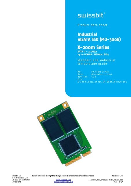
X-<strong>200m</strong> <strong>Series</strong> – Industrial MSATA Solid State Drive<br />
2GByte up to 32GByte (MO-300B)<br />
1 Feature summary<br />
Form factor:<br />
o Full-sized mSATA form factor<br />
o JEDEC MO-300B sized Solid State Drive (SSD)<br />
o 50.8mm x 29.85mm x 3.3mm<br />
o 52 pin PCI Express (PCIe) mini-connector (SATA II)<br />
Interface:<br />
o SATA Rev 2.6 - 3Gbit/s (1.5Gbit/s compatible)<br />
o mechanical identical to mini-PCIe and eeePC card connector,<br />
but different pinout<br />
Highly-integrated memory controller<br />
o max. UDMA6 supported<br />
o max. PIO mode 4, MDMA2 supported<br />
o SLC NAND Flash<br />
o Hardware BCH-code ECC (8 Bit correction per sector for SLC)<br />
o fix drive configuration<br />
Low-power CMOS technology<br />
3.3V ± 5% power supply<br />
optional activity LED and write protect switch on request<br />
No mechanical noise<br />
Wear Leveling: active wear leveling of static and dynamic data<br />
The wear leveling assures that dynamic data as well as static data is balanced evenly across the<br />
memory. With that the maximum write endurance of the device is guaranteed.<br />
High reliability<br />
o MTBF > 2,500,000 hours<br />
o Data reliability: < 1 non-recoverable error per 10 14 bits read<br />
High performance<br />
o Up to 300MB/s burst transfer rate in SATA II - 3.0Gb/sec<br />
o Sustained Write performance: up to 95MB/s<br />
o Sustained Read Performance: up to 120MB/s<br />
Available densities<br />
o 2GByte up to 32GByte (SLC NAND Flash)<br />
S.M.A.R.T. support<br />
2 Temperature ranges<br />
o Commercial Temperature range 0 … +70°C<br />
o Industrial Temperature range -40 … +85°C<br />
Life Cycle Management<br />
Controlled BOM<br />
RoHS compatible<br />
<strong>Swissbit</strong> AG <strong>Swissbit</strong> reserves the right to change products or specifications without notice. Revision: 1.20<br />
Industriestrasse 4-8<br />
CH-9552 Bronschhofen www.swissbit.com X-<strong>200m</strong>_data_sheet_SA-UxBR_Rev120.doc<br />
Switzerland industrial@swissbit.com Page 2 of 47
2 Contents<br />
1 FEATURE SUMMARY ................................................................................................................................................................... 2<br />
2 CONTENTS .................................................................................................................................................................................. 3<br />
3 ORDER INFORMATION ............................................................................................................................................................... 5<br />
3.1 AVAILABLE STANDARD PART NUMBERS ...................................................................................................................................... 5<br />
4 PRODUCT SPECIFICATION ........................................................................................................................................................... 6<br />
4.1 PHYSICAL DESCRIPTION .......................................................................................................................................................... 6<br />
4.2 SYSTEM PERFORMANCE ......................................................................................................................................................... 6<br />
4.3 ENVIRONMENTAL SPECIFICATIONS ............................................................................................................................................ 7<br />
4.4 PHYSICAL DIMENSIONS ......................................................................................................................................................... 7<br />
4.5 RELIABILITY ........................................................................................................................................................................ 7<br />
4.6 DRIVE GEOMETRY / CHS PARAMETER ....................................................................................................................................... 7<br />
5 ELECTRICAL INTERFACE .............................................................................................................................................................. 8<br />
5.1 ELECTRICAL DESCRIPTION ........................................................................................................................................................ 8<br />
5.2 ELECTRICAL SPECIFICATION ..................................................................................................................................................... 9<br />
6 ATA COMMAND DESCRIPTION.................................................................................................................................................. 10<br />
6.1 CHECK POWER MODE (98H OR E5H) .................................................................................................................................... 12<br />
6.2 ERASE SECTOR(S) (C0H) ..................................................................................................................................................... 12<br />
6.3 EXECUTE DRIVE DIAGNOSTIC (90H) ....................................................................................................................................... 12<br />
6.4 FLUSH CACHE (E7H) ........................................................................................................................................................... 13<br />
6.5 IDENTIFY DEVICE (ECH) ...................................................................................................................................................... 13<br />
6.6 IDLE (97H OR E3H) ........................................................................................................................................................... 20<br />
6.7 IDLE IMMEDIATE (95H OR E1H) ............................................................................................................................................ 20<br />
6.8 NOP (00H) .................................................................................................................................................................... 20<br />
6.9 READ BUFFER (E4H) ......................................................................................................................................................... 21<br />
6.10 READ DMA (C8H) ........................................................................................................................................................... 21<br />
6.11 READ MULTIPLE (C4H) ...................................................................................................................................................... 21<br />
6.12 READ NATIVE MAX ADDRESS (F8H) ...................................................................................................................................... 22<br />
6.13 READ SECTOR(S) (20H) ..................................................................................................................................................... 23<br />
6.14 READ VERIFY SECTOR(S) (40H OR 41H) ................................................................................................................................ 23<br />
6.15 REQUEST SENSE (03H) ...................................................................................................................................................... 23<br />
6.16 SECURITY DISABLE PASSWORD (F6H) ................................................................................................................................... 24<br />
6.17 SECURITY ERASE PREPARE (F3H) ......................................................................................................................................... 24<br />
6.18 SECURITY ERASE UNIT (F4H) .............................................................................................................................................. 25<br />
6.19 SECURITY FREEZE LOCK (F5H) ............................................................................................................................................ 25<br />
6.20 SECURITY SET PASSWORD (F1H) .......................................................................................................................................... 26<br />
6.21 SECURITY UNLOCK (F2H) .................................................................................................................................................... 27<br />
6.22 SET FEATURES (EFH) ........................................................................................................................................................ 27<br />
6.23 SET MAX ADDRESS (F9H)................................................................................................................................................... 29<br />
6.24 SET MULTIPLE MODE (C6H) .............................................................................................................................................. 30<br />
6.25 SLEEP (99H OR E6) ........................................................................................................................................................ 30<br />
6.26 S.M.A.R.T. (B0H) ........................................................................................................................................................ 31<br />
6.27 STANDBY (96H OR E2) ..................................................................................................................................................... 31<br />
6.28 STANDBY IMMEDIATE (94H OR E0H) .................................................................................................................................. 31<br />
6.29 TRANSLATE SECTOR (87H) ................................................................................................................................................. 32<br />
6.30 WRITE BUFFER (E8H) ...................................................................................................................................................... 32<br />
6.31 WRITE DMA (CAH) .......................................................................................................................................................... 32<br />
6.32 WRITE MULTIPLE COMMAND (C5H) ..................................................................................................................................... 33<br />
6.33 WRITE MULTIPLE WITHOUT ERASE (CDH) .............................................................................................................................. 33<br />
6.34 WRITE SECTOR(S) (30H) ................................................................................................................................................... 34<br />
6.35 WRITE SECTOR(S) WITHOUT ERASE (38H) ............................................................................................................................. 34<br />
7 S.M.A.R.T. FUNCTIONALITY ..................................................................................................................................................... 35<br />
7.1 S.M.A.R.T. ENABLE / DISABLE OPERATIONS ........................................................................................................................... 35<br />
7.2 S.M.A.R.T. RETURN STATUS ............................................................................................................................................... 35<br />
<strong>Swissbit</strong> AG <strong>Swissbit</strong> reserves the right to change products or specifications without notice. Revision: 1.20<br />
Industriestrasse 4-8<br />
CH-9552 Bronschhofen www.swissbit.com X-<strong>200m</strong>_data_sheet_SA-UxBR_Rev120.doc<br />
Switzerland industrial@swissbit.com Page 3 of 47
7.3 S.M.A.R.T. ENABLE / DISABLE ATTRIBUTE AUTOSAVE .............................................................................................................. 36<br />
7.4 S.M.A.R.T. SAVE ATTRIBUTE VALUES ................................................................................................................................... 36<br />
7.5 S.M.A.R.T. EXECUTE OFF-LINE IMMEDIATE ........................................................................................................................ 36<br />
7.6 S.M.A.R.T. READ DATA..................................................................................................................................................... 36<br />
8 PACKAGE MECHANICAL ........................................................................................................................................................... 39<br />
DECLARATION OF CONFORMITY .................................................................................................................................................. 41<br />
9 ROHS AND WEEE UPDATE FROM SWISSBIT ............................................................................................................................. 42<br />
10 PART NUMBER DECODER ....................................................................................................................................................... 44<br />
10.1 MANUFACTURER ............................................................................................................................................................... 44<br />
10.2 MEMORY TYPE ................................................................................................................................................................. 44<br />
10.3 PRODUCT TYPE ................................................................................................................................................................. 44<br />
10.4 DENSITY ......................................................................................................................................................................... 44<br />
10.5 PLATFORM ...................................................................................................................................................................... 44<br />
10.6 PRODUCT GENERATION ...................................................................................................................................................... 44<br />
10.7 MEMORY ORGANIZATION .................................................................................................................................................... 44<br />
10.8 TECHNOLOGY ................................................................................................................................................................... 44<br />
10.9 NUMBER OF FLASH CHIP ................................................................................................................................................... 44<br />
10.10 FLASH CODE .................................................................................................................................................................. 44<br />
10.11 TEMP. OPTION ................................................................................................................................................................ 45<br />
10.12 DIE CLASSIFICATION......................................................................................................................................................... 45<br />
10.13 PIN MODE .................................................................................................................................................................... 45<br />
10.14 DRIVE CONFIGURATION XYZ .............................................................................................................................................. 45<br />
10.15 OPTION ......................................................................................................................................................................... 45<br />
11 SWISSBIT MSATA SSD MARKING SPECIFICATION .................................................................................................................... 46<br />
11.1 TOP VIEW ......................................................................................................................................................................... 46<br />
12 REVISION HISTORY ................................................................................................................................................................. 47<br />
<strong>Swissbit</strong> AG <strong>Swissbit</strong> reserves the right to change products or specifications without notice. Revision: 1.20<br />
Industriestrasse 4-8<br />
CH-9552 Bronschhofen www.swissbit.com X-<strong>200m</strong>_data_sheet_SA-UxBR_Rev120.doc<br />
Switzerland industrial@swissbit.com Page 4 of 47
3 Order Information<br />
3.1 Available Standard part numbers<br />
FIX / SATA II/ PIO4, MDMA2, UDMA6<br />
Density Part Number<br />
2GB SFSA2048UxBR2TO-t-MS-2y6-STD<br />
4GB SFSA4096UxBR4TO-t-MS-2y6-STD<br />
8GB SFSA8192UxBR4TO-t-DT-2y6-STD<br />
16GB SFSA16GBUxBR4TO-t-QT-2y6-STD<br />
32GB SFSA32GBUxBR4TO-t-NC-2y6-STD<br />
Table 1: Standard product list<br />
x= depends on product generation;<br />
y= depends on FW revision<br />
t= C commercial temperature; =I industrial temperature<br />
<strong>Swissbit</strong> AG <strong>Swissbit</strong> reserves the right to change products or specifications without notice. Revision: 1.20<br />
Industriestrasse 4-8<br />
CH-9552 Bronschhofen www.swissbit.com X-<strong>200m</strong>_data_sheet_SA-UxBR_Rev120.doc<br />
Switzerland industrial@swissbit.com Page 5 of 47
4 Product Specification<br />
The Solid State Drive (SSD) is a small form factor 50.8mm x 29.85 mm x 3.3mm) non-volatile memory drive<br />
which provides high capacity data storage. The SSDs are designed after the JEDEC MO-300B standard. It has a<br />
standard combined connector with SATA and power/control part. The connector is mechanical identical with<br />
eeePC card connector, but has different pinout. The card works at a supply voltage of 3.3V.<br />
The drive with the SATA interface operates in Mode 2.0 (1.5 or 3.0 Gb/s burst).<br />
The drive has an internal intelligent controller which manages interface protocols, data storage and retrieval as<br />
well as hardware BCH-code Error Correction Code (ECC), defect handling, diagnostics and clock control.<br />
The wear leveling mechanism assures an equal usage of the Flash memory cells to extend the life time.<br />
The hardware BCH-code ECC allows to detect and correct 8 random bits per 528 Bytes.<br />
The drive has a voltage detector and a powerful power-loss management feature to prevent data corruption<br />
after power-down.<br />
The specification has been realized and approved by the ATA/ATAPI-7 specification.<br />
The system highlights are shown in Table 2 …Table 9.<br />
Related Documentation<br />
Serial Transport Protocols and Physical Interconnect (ATA/ATAPI-7)<br />
AT Attachment Interface Document, American National Standards Institute, X3.221-1994<br />
JEDEC MO-300 standard<br />
4.1 Physical description<br />
The SSD contains a flash controller and Flash memory modules. The controller interfaces with a host system<br />
allowing data to be written to and read from the Flash memory modules.<br />
The SSD has a PCIe mini connector with SATA interface. Figure 1 and Figure 2 (page 39) show SSD dimensions and<br />
connector location.<br />
4.2 System Performance<br />
Table 2: System Performance (measured) UDMA5<br />
System Performance Typ. Max. Unit<br />
Data transfer Rate (SATA burst (1.5 or 3.0Gb/s)) 150 or 300 300<br />
Sustained Sequential Read<br />
128kB Block size<br />
Sustained Sequential Write<br />
128kB Block size<br />
Sustained Sequential Read<br />
4kB Block size<br />
Sustained Sequential Write<br />
4kB Block size<br />
Sustained Random Read<br />
4kB Block size<br />
2GB (2ch) 56 (1) 60<br />
4GB 100 (1) 110<br />
8…16GB 110 (1) 120<br />
32GB 93 (1) 100<br />
2GB (2ch) 25 (1) 26<br />
4GB 46 (1) 47<br />
8…16GB 87 (1) 95<br />
32GB 76 (1) 90<br />
2GB 24 (1) 25<br />
4GB 27 (1) 28<br />
8…16GB 28 (1) 30<br />
32GB 25 (1) 28<br />
2GB (2ch) 17 (1) 18<br />
4GB 20 (1) 22<br />
8…16GB 21 (1) 23<br />
32GB 19 (1) 21<br />
2GB (2ch) 11 (1) 12<br />
4…8GB 11 (1) 12<br />
16GB 9 (1) 11<br />
8…16GB 6 (1) 8<br />
32GB 5.5 (1) 7<br />
2GB (2ch) 0.07<br />
Sustained Random Write<br />
4kB Block size<br />
(1)(2) 0.10<br />
4GB 0.06 (1)(2) 0.09<br />
8…16GB 0.05 (1)(2) 0.08<br />
32GB 0.05 (1)(2) 0.08<br />
1. All values refer to Toshiba Flash chips (see part number) in UDMA5 mode (SATA 3.0Gbit/s) with Sequential write/read test (256<br />
sectors multiple commands) and sequential and random write/read test (8 sectors multiple commands). Sustained Speed depends<br />
on flash type and number, file/cluster size, and burst speed.<br />
2. The typical random write speed values are really random access across the whole drive. Random write values in file systems are<br />
much larger.<br />
<strong>Swissbit</strong> AG <strong>Swissbit</strong> reserves the right to change products or specifications without notice. Revision: 1.20<br />
Industriestrasse 4-8<br />
CH-9552 Bronschhofen www.swissbit.com X-<strong>200m</strong>_data_sheet_SA-UxBR_Rev120.doc<br />
Switzerland industrial@swissbit.com Page 6 of 47<br />
MB/s<br />
MB/s<br />
MB/s
4.3 Environmental Specifications<br />
4.3.1 Recommended Operating Conditions<br />
Table 3: Recommended Operating Conditions<br />
Parameter Value<br />
Commercial Operating Temperature 0°C to 70°C<br />
Industrial Operating Temperature -40°C to 85°C<br />
Power Supply VCC Voltage 3.3V ±5%<br />
Table 4: Current consumption (1)<br />
Current Consumption (type) 3.3V Unit<br />
Read (typ/max) 300/420<br />
Write (typ/max) 300/370<br />
mA<br />
Sleep/Idle Mode (typ/max) 200/220<br />
1. All values are typical at 25° C and nominal supply voltage and refer to SATAII performance test random pattern for a 64GByte SSD.<br />
4.3.2 Recommended Storage Conditions<br />
Table 5: Recommended Storage Conditions<br />
Parameter Value<br />
Commercial Storage Temperature -50°C to 100°C<br />
Industrial Storage Temperature -50°C to 100°C<br />
4.3.3 Shock, Vibration, and Humidity<br />
Table 6: Shock, Vibration, and Humidity<br />
Parameter Value<br />
Humidity (non-condensing) 85% RH 85°C, 1000 hrs (JEDEC JESD22, method A101-B)<br />
Vibration 20G Peak, 10…2000Hz<br />
Shock 1500G, 0.5ms duration, half sine wave<br />
4.4 Physical Dimensions<br />
Table 7: Physical Dimensions<br />
Physical Dimensions Unit<br />
Length 50.8±0.15<br />
Width 29.85±0.15<br />
mm<br />
Thickness max 3.3<br />
Weight (typ.) 7 g<br />
4.5 Reliability<br />
Table 8: System Reliability and Maintenance (1)<br />
Parameter Value<br />
MTBF (at 25°C) > 2,500,000 hours<br />
Data Reliability < 1 Non-Recoverable Error per 10 14 bits Read<br />
Data Retention 10 years (JESD47)<br />
1. Dependent on final system qualification data.<br />
4.6 Drive geometry / CHS parameter<br />
Table 9: SSD capacity specification<br />
Capacity Default_cylinders Default_heads Default_sectors Sectors_drive Total addressable Bytes<br />
2GB 3,886 16 63 3,896,928 1,995,227,136<br />
4GB 7,732 16 63 7,793,856 3,990,454,272<br />
8GB 15,498 16 63 15,621,984 7,998,455,808<br />
16GB 16,383*) 16 63 31,277,056 16,013,852,672<br />
32GB 16,383*) 16 63 62,586,880 32,044,482,560<br />
*) The CHS access is limited to about 8GB. Above 8GB the drive must be addressed in LBA mode.<br />
<strong>Swissbit</strong> AG <strong>Swissbit</strong> reserves the right to change products or specifications without notice. Revision: 1.20<br />
Industriestrasse 4-8<br />
CH-9552 Bronschhofen www.swissbit.com X-<strong>200m</strong>_data_sheet_SA-UxBR_Rev120.doc<br />
Switzerland industrial@swissbit.com Page 7 of 47
5 Electrical interface<br />
5.1 Electrical description<br />
The Mini-SATA connector is the same as the miniPCIE and eeePC card connector, but the pinout is different.<br />
Table 10: Pin Assignment, name, and description<br />
Description Assignment Pin Pin Assignment Description<br />
No Connect N/A 1 2 +3.3V 3.3V Source<br />
No Connect N/A 3 4 GND Return Current Path<br />
No Connect N/A 5 6 +1.5V No Connect<br />
No Connect N/A 7 8 N/A No Connect<br />
Return Current Path GND 9 10 N/A No Connect<br />
No Connect N/A 11 12 N/A No Connect<br />
No Connect N/A 13 14 N/A No Connect<br />
Return Current Path GND 15 16 N/A No Connect<br />
No Connect N/A 17 18 GND Return Current Path<br />
No Connect N/A 19 20 N/A No Connect<br />
Return Current Path GND 21 22 N/A No Connect<br />
+ SATA differential transmit signal B+ 23 24 3.3V 3.3V Source<br />
- SATA differential transmit signal B- 25 26 GND Return Current Path<br />
Return Current Path GND 27 28 1.5V No Connect<br />
Return Current Path GND 29 30 N/A No Connect<br />
- SATA differential receive signal A- 31 32 N/A No Connect<br />
+ SATA differential receive signal A+ 33 34 GND Return Current Path<br />
Return Current Path GND 35 36 N/A No Connect<br />
Return Current Path GND 37 38 N/A No Connect<br />
3.3V Source 3.3V 39 40 GND Return Current Path<br />
3.3V Source 3.3V 41 42 N/A No Connect<br />
Return Current Path GND 43 44 N/A No Connect<br />
No Connect Reserved 45 46 N/A No Connect<br />
No Connect Reserved 47 48 +1.5V No Connect<br />
Device activity / LED DA 49 50 N/A optional Return<br />
(optional) *)<br />
Pulled to GND by Device Presence<br />
detection<br />
51 52 3.3V<br />
Current Path**)<br />
3.3V Source<br />
*) Device Activity Pin is low in idle mode and high (flickering) during data transfer.<br />
It can be optional disconnected on the module or the pin can configured without driving,<br />
only pull up resistor on request.<br />
In firmware revision “1” (part number -216-STD) this pin is driven low and high If this pin is grounded<br />
by the host, a current goes through this pin.<br />
In firmware “2” and higher this pin is only driven low as optional specified in the SATA-Specification<br />
“SerialATA_Revision_3_0_Gold”<br />
**) In standard products pin50 is not connected on the SSD to prevent power short circuit if connected to an<br />
eeePC card connector, but could be optional connected to GND<br />
<strong>Swissbit</strong> AG <strong>Swissbit</strong> reserves the right to change products or specifications without notice. Revision: 1.20<br />
Industriestrasse 4-8<br />
CH-9552 Bronschhofen www.swissbit.com X-<strong>200m</strong>_data_sheet_SA-UxBR_Rev120.doc<br />
Switzerland industrial@swissbit.com Page 8 of 47
5.2 Electrical Specification<br />
Table 11 defines the DC Characteristics of the SSD. Unless otherwise stated, conditions are:<br />
Vcc = 3.3V ± 5%<br />
0°C to +70°C<br />
Table 11: Absolute Maximum Conditions<br />
Parameter Symbol Conditions<br />
Input Power VCC -0.3V to 3.6V<br />
<strong>Swissbit</strong> AG <strong>Swissbit</strong> reserves the right to change products or specifications without notice. Revision: 1.20<br />
Industriestrasse 4-8<br />
CH-9552 Bronschhofen www.swissbit.com X-<strong>200m</strong>_data_sheet_SA-UxBR_Rev120.doc<br />
Switzerland industrial@swissbit.com Page 9 of 47
6 ATA command description<br />
This section provides information on the ATA commands supported by the SSD. The commands are issued to the<br />
ATA by loading the required registers in the command block with the supplied parameter, and then writing the<br />
command code to the register.<br />
ATA Command Flow<br />
DDMAI0: DMA_in State This state is activated when the device receives a DMA data-in command or the<br />
transmission of one or more data FIS is required to complete the command. When in this<br />
state, the device shall prepare the data for transfer of a data FIS to the host.<br />
Transition DDMAI0:1 When the device has the data ready to transfer a data FIS, the device shall transition to<br />
the DDMAI1: Send_data state. Transition DDMAI0:2 When the device has transferred all of<br />
the data requested by this command or has encountered an error that causes the<br />
command to abort before completing the transfer of the requested data, then the device<br />
shall transition to the DDMAI2: Send_status state.<br />
DDMAI1: Send_data This state is activated when the device has the data ready to transfer a data FIS to the<br />
host. When in this state, the device shall request that the Transport layer transmit a<br />
data FIS containing the data. The device command layer shall request a Data FIS size of<br />
no more than 2,048 Dwords (8KB).<br />
Transition DDMAI1:1 When the data FIS has been transferred, the device shall transition to the DMAOI0:<br />
DMA_in state.<br />
DDMAI2: Send_status This state is activated when the device has transferred all of the data requested by the<br />
command or has encountered an error that causes the command to abort before<br />
completing the transfer of the requested data. When in this state, the device shall<br />
request that the Transport layer transmit a Register FIS with the register content as<br />
described in the command description in the ATA/ATAPI-6 standard and the I bit set to<br />
one.<br />
Transition DDMAI2:1 When the FIS has been transmitted, the device shall transition to the DI0: Device_idle<br />
state.<br />
<strong>Swissbit</strong> AG <strong>Swissbit</strong> reserves the right to change products or specifications without notice. Revision: 1.20<br />
Industriestrasse 4-8<br />
CH-9552 Bronschhofen www.swissbit.com X-<strong>200m</strong>_data_sheet_SA-UxBR_Rev120.doc<br />
Switzerland industrial@swissbit.com Page 10 of 47
For reasons of backward compatibility some commands are implemented as ‘no operation’ NOP.<br />
Table 12 summarizes the Drive command set with the paragraphs that follow describing the individual<br />
commands and the task file for each.<br />
Table 12: ATA Command Set (1)<br />
Command Code FR SC SN CY DH LBA<br />
Check Power Mode E5h or 98h D<br />
Erase Sector(s) (CFA) C0h Y Y Y Y Y<br />
Execute Drive Diagnostic 90h D<br />
Flush cache E7h D<br />
Identify Drive ECh D<br />
Idle E3h or 97h Y D<br />
Idle Immediate E1h or 95h D<br />
NOP 00h D<br />
Read Buffer E4h D<br />
Read DMA C8 Y Y Y Y Y<br />
Read Multiple C4h Y Y Y Y Y<br />
Read native max address F8h D<br />
Read Sector(s) 20h Y Y Y Y Y<br />
Read Verify Sector(s) 40h or 41h Y Y Y Y Y<br />
Request Sense (CFA) 03h D<br />
Security Disable Password F6h D<br />
Security Erase Prepare F3h D<br />
Security Erase Unit F4h D<br />
Security Freeze Lock F5h D<br />
Security Set Password F1h D<br />
Security Unlock F2h D<br />
Set Features EFh Y D<br />
Set max address (with set password) F9h Y Y Y Y Y<br />
Set Multiple Mode C6h Y D<br />
Sleep E6h or 99h D<br />
S.M.A.R.T. B0h Y Y Y D<br />
Standby E2h or 96h D<br />
Standby Immediate E0h or 94h D<br />
Translate Sector (CFA) 87h Y Y Y Y Y<br />
Write Buffer E8h D<br />
Write DMA CA Y Y Y Y Y<br />
Write Multiple C5h Y Y Y Y Y<br />
Write Multiple w/o Erase (CFA) CDh Y Y Y Y Y<br />
Write Sector(s) 30h Y Y Y Y Y<br />
Write Sector(s) w/o Erase (CFA) 38h Y Y Y Y Y<br />
1. FR = Features Register, SC = Sector Count Register, SN = Sector Number Register, CY = Cylinder Registers,<br />
DH = Drive/Head Register, LBA = Logical Block Address Mode Supported (see command descriptions for use),<br />
Y – The register contains a valid parameter for this command. For the Drive/Head Register Y means both the Drive and head<br />
parameters are used.<br />
D – only the Drive parameter is valid and not the head parameter C – the register contains command specific data (see<br />
command descriptors for use).<br />
<strong>Swissbit</strong> AG <strong>Swissbit</strong> reserves the right to change products or specifications without notice. Revision: 1.20<br />
Industriestrasse 4-8<br />
CH-9552 Bronschhofen www.swissbit.com X-<strong>200m</strong>_data_sheet_SA-UxBR_Rev120.doc<br />
Switzerland industrial@swissbit.com Page 11 of 47
6.1 Check Power Mode (98h or E5h)<br />
This command checks the power mode.<br />
Issuing the command while the Drive is in Standby mode, is about to enter Standby, or is exiting Standby, the<br />
command will set BSY, set the Sector Count Register to 00h, clear BSY and generate an interrupt.<br />
Issuing the command when the Drive is in Idle mode will set BSY, set the Sector Count Register to FFh, clear BSY<br />
and generate an interrupt.<br />
Table 13 defines the Byte sequence of the Check Power Mode command.<br />
Table 13: Check Power Mode<br />
Task File Register 7 6 5 4 3 2 1 0<br />
COMMAND 98h or E5h<br />
DRIVE/HEAD nu nu nu D nu<br />
CYLINDER HI nu<br />
CYLINDER LOW nu<br />
SECTOR NUM nu<br />
SECTOR COUNT nu<br />
FEATURES nu<br />
6.2 Erase Sector(s) (C0h)<br />
This command is used to pre-erase and condition data sectors prior to a Write Sector without Erase command or<br />
a Write Multiple Without Erase command. There is no data transfer associated with this command but a Write<br />
Fault error status can occur. Table 14 defines the Byte sequence of the Erase Sector command.<br />
Table 14: Erase Sector(s)<br />
Task File Register 7 6 5 4 3 2 1 0<br />
COMMAND C0h<br />
DRIVE/HEAD nu L nu D H[3:0] or LBA[27:24] of the starting sector/LBA<br />
CYLINDER HI Cylinder[15:8] or LBA[23:16] of the first sector/LBA to erase<br />
CYLINDER LOW Cylinder[7:0] or LBA[15:8] of the first sector/LBA to erase<br />
SECTOR NUM Sector[7:0] or LBA[7:0] of the first sector/LBA to erase<br />
SECTOR COUNT The number of sectors/logical blocks to erase<br />
FEATURES nu<br />
6.3 Execute Drive Diagnostic (90h)<br />
This command performs the internal diagnostic tests implemented by the Drive.<br />
The Drive bit is ignored and the diagnostic command is executed by both the Master and the Slave with the<br />
Master responding with the status for both devices.<br />
Table 15 defines the Execute Drive Diagnostic command Byte sequence. The Diagnostic codes shown in Table 16<br />
are returned in the Error Register at the end of the command.<br />
Table 15: Execute Drive Diagnostic<br />
Task File Register 7 6 5 4 3 2 1 0<br />
COMMAND 90h<br />
DRIVE/HEAD nu nu nu D nu<br />
CYLINDER HI nu<br />
CYLINDER LOW nu<br />
SECTOR NUM nu<br />
SECTOR COUNT nu<br />
FEATURES nu<br />
Table 16: Diagnostic Codes<br />
Code Error Type<br />
01h No Error Detected<br />
02h Formatter Device Error<br />
03h Sector Buffer Error<br />
04h ECC Circuitry Error<br />
05h Controlling Microprocessor Error<br />
<strong>Swissbit</strong> AG <strong>Swissbit</strong> reserves the right to change products or specifications without notice. Revision: 1.20<br />
Industriestrasse 4-8<br />
CH-9552 Bronschhofen www.swissbit.com X-<strong>200m</strong>_data_sheet_SA-UxBR_Rev120.doc<br />
Switzerland industrial@swissbit.com Page 12 of 47
6.4 Flush Cache (E7h)<br />
This command causes the drive to complete writing data from its cache. The drive returns status with RDY=1 and<br />
DSC=1 after the data in the write cache buffer is written to the media. If the drive does not support the Flush<br />
Cache command, the drive shall return command aborted.<br />
Table 17: Flush Cache<br />
Task File Register 7 6 5 4 3 2 1 0<br />
COMMAND E7h<br />
DRIVE/HEAD nu nu nu D nu<br />
CYLINDER HI nu<br />
CYLINDER LOW nu<br />
SECTOR NUM nu<br />
SECTOR COUNT nu<br />
FEATURES nu<br />
6.5 Identify Device (ECh)<br />
The Identify Device command enables the host to receive parameter information from the Drive. This command<br />
has the same protocol as the Read Sector(s) command. Table 18 defines the Identify Device command Byte<br />
sequence. All reserved bits or Words are zero.<br />
Table 19 shows the definition of each field in the Identify Drive Information.<br />
Table 18: Identify Device<br />
Task File Register 7 6 5 4 3 2 1 0<br />
COMMAND ECh<br />
DRIVE/HEAD nu nu nu D nu<br />
CYLINDER HI nu<br />
CYLINDER LOW nu<br />
SECTOR NUM nu<br />
SECTOR COUNT nu<br />
FEATURES nu<br />
<strong>Swissbit</strong> AG <strong>Swissbit</strong> reserves the right to change products or specifications without notice. Revision: 1.20<br />
Industriestrasse 4-8<br />
CH-9552 Bronschhofen www.swissbit.com X-<strong>200m</strong>_data_sheet_SA-UxBR_Rev120.doc<br />
Switzerland industrial@swissbit.com Page 13 of 47
Table 19: Identify Device Information<br />
Word<br />
Address<br />
Default<br />
Value<br />
Total<br />
Bytes<br />
Data Field Type Information<br />
0 044Ah* 2 Standard Configuration FIX (optional 848Ah for removable)<br />
1 XXXXh 2 Default number of cylinders (obsolete)<br />
2 0000h 2 Reserved<br />
3 00XXh 2 Default number of heads (obsolete)<br />
4 0000h 2 Obsolete<br />
5 XXXXh 2 Obsolete<br />
6 XXXXh 2 Default number of sectors per track (obsolete)<br />
7-8 XXXXh 4 Number of sectors per Drive (Word 7 = MSW, Word 8 = LSW)<br />
9 0000h 2 Obsolete<br />
10-19 aaaa 20 Serial number in ASCII (right justified)<br />
20 0002h 2 Buffer type (dual ported multi-sector) retired<br />
21 0002h* 2 Buffer Size in 512byte increment (obsolete)<br />
22 000Xh 2 Reserved<br />
23-26 YYYY* 8 Firmware revision in ASCII. Big Endian Byte Order in Word<br />
27-46 YYYY* 40 Model number in ASCII (right justified (“SFSAxxxxUxBRxxx-x-xx-xxx-xxx”)<br />
47 8001h 2 Maximum number of sectors on Read/Write Multiple command<br />
48 0000h 2 Double word not supported<br />
49<br />
0F00h*<br />
0E00h*<br />
2<br />
Capabilities with DMA, LBA, IORDY supported<br />
without DMA LBA, IORDY supported<br />
50 4000h 2 Capabilities<br />
51 0200h 2 PIO data transfer cycle timing mode 2<br />
52 0000h 2 Obsolete<br />
53 0007h* 2 Field validity (Bytes 54-58, 64-70, 88)<br />
54 XXXXh 2 Current numbers of cylinders (obsolete)<br />
55 XXXXh 2 Current numbers of heads (obsolete)<br />
56 XXXXh 2 Current sectors per track (obsolete)<br />
57-58 XXXXh 4 Current capacity in sectors (LBAs)(Word 57 = LSW, Word 58 = MSW) (obsolete)<br />
59 010Xh* 2 Multiple sector setting (can be changed by host).<br />
60-61 XXXXh 4 Total number of sectors addressable in LBA Mode<br />
62 0000h 2 Obsolete<br />
63<br />
0007h*<br />
0000h*<br />
2<br />
Multi-Word DMA transfer support and selection (can be changed by host).<br />
no multi-word DMA<br />
64 0003h 2 Advanced PIO modes 3 and 4 supported<br />
65 0078h* 2 Minimum Multi-Word DMA transfer cycle time per Word.<br />
66 0078h* 2 Recommended Multi-Word DMA transfer cycle time.<br />
67 0078h* 2 Minimum PIO transfer cycle time without flow control<br />
68 0078h* 2 Minimum PIO transfer cycle time with IORDY flow control<br />
69-75 0000h 14 Reserved<br />
76 0006h 2 SATA Capabilities<br />
77 0000h 2 Reserved<br />
78 0008h 2 SATA Feature support<br />
79 0000h* 2 SATA Features enabled (can be changed by host)<br />
80-81<br />
0080h<br />
0000h<br />
742Bh*<br />
4 ATA/ATAPI version 7<br />
82 -84 5500h*<br />
4002h*<br />
7429h*<br />
6 Features/command sets supported<br />
85-87 1400h*<br />
4002h*<br />
6 Features/command sets enabled (can change in operation)<br />
88 207F* 2 UDMA Mode Supported 0,1,2,3,4,5,6 and Selected 5 (changes in operation)<br />
89 0003* 2 Time for security erase unit completion (e.g. 6 minutes)<br />
90-91 0000h* 4 Reserved<br />
92 FFFE* 2 Master Password Revision Code<br />
93-127 0000h* 70 Reserved<br />
128 0001h* 2 Security Status (changes in operation)<br />
129-159 XXXXh 62 Vendor specific (e.g.”<strong>Swissbit</strong> SSD”)<br />
160 0000h* 2 Max. current<br />
161-216 0000h 112 Reserved<br />
217 0001h* 2 Nominal Media Rotation Rate: Solid State Device<br />
218-255 0000h 76 Reserved<br />
* Standard values for full functionality, depending on configuration<br />
XXXX Depending on drive capacity and drive geometry<br />
YYYY Depending on drive configuration<br />
<strong>Swissbit</strong> AG <strong>Swissbit</strong> reserves the right to change products or specifications without notice. Revision: 1.20<br />
Industriestrasse 4-8<br />
CH-9552 Bronschhofen www.swissbit.com X-<strong>200m</strong>_data_sheet_SA-UxBR_Rev120.doc<br />
Switzerland industrial@swissbit.com Page 14 of 47
6.5.1 Word 0: General Configuration<br />
This field indicates the general characteristics of the device.<br />
The default value for Word 0 is set to 045Ah.<br />
Some operating systems require Bit 6 of Word 0 to be set to ‘1’ (Non-removable device) to use the drive as the<br />
root storage device.<br />
6.5.2 Word 1: Default Number of Cylinders<br />
This field contains the number of translated cylinders in the default translation mode. This value will be the<br />
same as the number of cylinders.<br />
6.5.3 Word 3: Default Number of Heads<br />
This field contains the number of translated heads in the default translation mode.<br />
6.5.4 Word 6: Default Number of Sectors per Track<br />
This field contains the number of sectors per track in the default translation mode.<br />
6.5.5 Word 7-8: Number of Sectors per Drive<br />
This field contains the number of sectors per Drive. This double Word value is also the first invalid address in LBA<br />
translation mode.<br />
6.5.6 Word 10-19: Memory Drive Serial Number<br />
The contents of this field are right justified and padded without spaces (20h).<br />
6.5.7 Word 23-26: Firmware Revision<br />
This field contains the revision of the firmware for this product.<br />
6.5.8 Word 27-46: Model Number<br />
This field contains the model number for this product and is left justified and padded with spaces (20h).<br />
6.5.9 Word 47: Read/Write Multiple Sector Count<br />
This field contains the maximum number of sectors that can be read or written per interrupt using the Read<br />
Multiple or Write Multiple commands.<br />
6.5.10 Word 49: Capabilities<br />
Bit 13 Standby Timer: is set to ’0’ to indicate that the Standby timer operation is defined by the<br />
manufacturer.<br />
Bit 11: IORDY Supported<br />
If bit 11 is set to 1 then this drive supports IORDY operation.<br />
If bit 11 is set to 0 then this drive may support IORDY operation.<br />
Bit 10: IORDY may be disabled<br />
If bit 10 is set to 1 then IODRDY may be disabled.<br />
Bit 9 LBA support: drive support LBA mode addressing.<br />
Bit 8 DMA Support: Read/Write DMA commands are supported.<br />
6.5.11 Word 51: PIO Data Transfer Cycle Timing Mode<br />
This field defines the mode for PIO data transfer. For backward compatibility with BIOSs written before Word 64<br />
was defined for advanced modes, a device reports in Word 51, the highest original PIO mode it can support (PIO<br />
mode 0, 1 or 2). Bits 15-8: are set to 02H.<br />
6.5.12 Word 53: Translation Parameter Valid<br />
Bit 0: is set to ‘1’ to indicate that Words 54 to 58 are valid<br />
Bit 1: is set to ‘1’ to indicate that Words 64 to 70 are valid<br />
Bit 2 shall be set to 1 indicating that word 88 is valid and reflects the supported UDMA<br />
<strong>Swissbit</strong> AG <strong>Swissbit</strong> reserves the right to change products or specifications without notice. Revision: 1.20<br />
Industriestrasse 4-8<br />
CH-9552 Bronschhofen www.swissbit.com X-<strong>200m</strong>_data_sheet_SA-UxBR_Rev120.doc<br />
Switzerland industrial@swissbit.com Page 15 of 47
6.5.13 Word 54-56: Current Number of Cylinders, Heads, Sectors/Track<br />
These fields contain the current number of user addressable Cylinders, Heads, and Sectors/Track in the current<br />
translation mode.<br />
6.5.14 Word 57-58: Current Capacity<br />
This field contains the product of the current cylinders, heads and sectors.<br />
6.5.15 Word 59: Multiple Sector Setting<br />
Bits 15-9 are reserved and must be set to ‘0’.<br />
Bit 8 is set to ‘1’, to indicate that the Multiple Sector Setting is valid.<br />
Bits 7-0 are the current setting for the number of sectors to be transferred for every interrupt, on<br />
Read/Write Multiple commands; the only values returned are ‘00h’ or ‘01h’.<br />
6.5.16 Word 60-61: Total Sectors Addressable in LBA Mode<br />
This field contains the number of sectors addressable for the Drive in LBA mode only.<br />
6.5.17 Word 63: Multi-Word DMA transfer<br />
Bits 15 through 8 of word 63 of the Identify Device parameter information is defined as the Multiword DMA mode<br />
selected field. If this field is supported, bit 1 of word 53 shall be set to one. This field is bit significant. Only one<br />
of bits may be set to one in this field by the drive to indicate the multiword DMA mode which is currently<br />
selected.<br />
Of these bits, bits 15 through 11 are reserved. Bit 8, if set to one, indicates that Multiword DMA mode 0 has been<br />
selected. Bit 9, if set to one, indicates that Multiword DMA mode 1 has been selected. Bit 10, if set to one,<br />
indicates that Multiword DMA mode 2 has been selected.<br />
Selection of Multiword DMA modes 3 and above are specific to Drive are as described in Word 163.<br />
Bits 7 through 0 of word 63 of the Identify Device parameter information is defined as the Multiword DMA data<br />
transfer supported field. If this field is supported, bit 1 of word 53 shall be set to one. This field is bit significant.<br />
Any number of bits may be set to one in this field by the drive to indicate the Multiword DMA modes it is<br />
capable of supporting.<br />
Of these bits, bits 7 through 2 are reserved. Bit 0, if set to one, indicates that the drive supports Multiword DMA<br />
mode 0. Bit 1, if set to one, indicates that the drive supports Multiword DMA modes 1 and 0. Bit 2, if set to one,<br />
indicates that the Drive supports Multiword DMA modes 2, 1 and 0.<br />
Support for Multiword DMA modes 3 and above are specific to Drive are reported in word 163 as described in<br />
Word 163.<br />
6.5.18 Word 64: Advanced PIO transfer modes supported<br />
This field is bit significant. Any number of bits may be set to ‘1’ in this field by the drive to indicate the<br />
advanced PIO modes it is capable of supporting.<br />
Bits 7-2 are reserved for future advanced PIO modes.<br />
Bit 1 is set to ‘1’, indicates that the Drive supports PIO mode 4.<br />
Bit 0 is set to ‘1’ to indicate that the Drive supports PIO mode 3.<br />
Support for PIO modes 5 and above are specific to Drive are reported in word 163 as described in Word 163.<br />
6.5.19 Word 65: Minimum Multi-Word DMA transfer cycle time<br />
Word 65 of the parameter information of the Identify Device command is defined as the minimum Multiword<br />
DMA transfer cycle time. This field defines, in nanoseconds, the minimum cycle time that, if used by the host,<br />
the Drive guarantees data integrity during the transfer.<br />
If this field is supported, bit 1 of word 53 shall be set to one. The value in word 65 shall not be less than the<br />
minimum cycle time for the fastest DMA mode supported by the device. This field shall be supported by all<br />
Drives supporting DMA modes 1 and above. If bit 1 of word 53 is set to one, but this field is not supported, the<br />
Drive shall return a value of zero in this field.<br />
6.5.20 Word 66: Recommended Multi-Word DMA transfer cycle time<br />
Word 66 of the parameter information of the Identify Device command is defined as the recommended<br />
Multiword DMA transfer cycle time. This field defines, in nanoseconds, the cycle time that, if used by the host,<br />
may optimize the data transfer from by reducing the probability that the Drive will need to negate the DMARQ<br />
signal during the transfer of a sector.<br />
<strong>Swissbit</strong> AG <strong>Swissbit</strong> reserves the right to change products or specifications without notice. Revision: 1.20<br />
Industriestrasse 4-8<br />
CH-9552 Bronschhofen www.swissbit.com X-<strong>200m</strong>_data_sheet_SA-UxBR_Rev120.doc<br />
Switzerland industrial@swissbit.com Page 16 of 47
If this field is supported, bit 1 of word 53 shall be set to one. The value in word 66 shall not be less than the<br />
value in word 65. This field shall be supported by all Drives supporting DMA modes 1 and above. If bit 1 of word<br />
53 is set to one, but this field is not supported, the Drive shall return a value of zero in this field.<br />
6.5.21 Word 67: Minimum PIO transfer cycle time without flow control<br />
Word 67 of the parameter information of the Identify Device command is defined as the minimum PIO transfer<br />
without flow control cycle time. This field defines, in nanoseconds, the minimum cycle time that, if used by the<br />
host, the Drive guarantees data integrity during the transfer without utilization of flow control.<br />
If this field is supported, Bit 1 of word 53 shall be set to one.<br />
Any Drive that supports PIO mode 3 or above shall support this field, and the value in word 67 shall not be less<br />
than the value reported in word 68.<br />
If bit 1 of word 53 is set to one because a Drive supports a field in words 64-70 other than this field and the<br />
Drive does not support this field, the Drive shall return a value of zero in this field.<br />
6.5.22 Word 68: Minimum PIO transfer cycle time with IORDY<br />
Word 68 of the parameter information of the Identify Device command is defined as the minimum PIO transfer<br />
with IORDY flow control cycle time. This field defines, in nanoseconds, the minimum cycle time that the Drive<br />
supports while performing data transfers while utilizing IORDY flow control.<br />
If this field is supported, Bit 1 of word 53 shall be set to one.<br />
Any Drive that supports PIO mode 3 or above shall support this field, and the value in word 68 shall be the<br />
fastest defined PIO mode supported by the Drive.<br />
If bit 1 of word 53 is set to one because a Drive supports a field in words 64-70 other than this field and the<br />
Drive does not support this field, the Drive shall return a value of zero in this field.<br />
6.5.23 Word 76: Serial ATA Capabilities<br />
Bit 15:11 Reserved<br />
Bit 10 1 = Supports Phy Event Counters<br />
Bit 9 1 = Supports receipt of host initiated power management requests<br />
Bit 8 1 = Supports native Command Queuing<br />
Bit 7:3 Reserved for future SATA signaling speed grades<br />
Bit 2 1 = Supports SATA Gen2 Signaling Speed (3.0Gb/s)<br />
Bit 1 1 = Supports SATA Gen1 Signaling Speed (1.5Gb/s)<br />
Bit 0 Shall be cleared to zero<br />
6.5.24 Word 78: SATA Feature support<br />
Bit 15-7 Reserved<br />
Bit 6 1 = Supports software settings preservation<br />
Bit 5 1 = Supports asynchronous notification<br />
Bit 4 1 = Supports in-order data delivery<br />
Bit 3 1 = Device supports initiating interface power management<br />
Bit 2 1 = Supports DMA Setup Auto-Activate optimization<br />
Bit 1 1 = Supports non-zero buffer offsets<br />
Bit 0 Shall be cleared to zero<br />
6.5.25 Word 79: SATA Features enabled<br />
Bit 15-7 Reserved<br />
Bit 6 1 = Supports software settings preservation enabled<br />
Bit 5 1 = Supports asynchronous notification enabled<br />
Bit 4 1 = Supports in-order data delivery enabled<br />
Bit 3 1 = Device supports initiating interface power management enabled<br />
Bit 2 1 = Supports DMA Setup Auto-Activate optimization enabled<br />
Bit 1 1 = Supports non-zero buffer offsets enabled<br />
Bit 0 Shall be cleared to zero<br />
<strong>Swissbit</strong> AG <strong>Swissbit</strong> reserves the right to change products or specifications without notice. Revision: 1.20<br />
Industriestrasse 4-8<br />
CH-9552 Bronschhofen www.swissbit.com X-<strong>200m</strong>_data_sheet_SA-UxBR_Rev120.doc<br />
Switzerland industrial@swissbit.com Page 17 of 47
6.5.26 Words 82-84: Features/command sets supported<br />
Words 82, 83, and 84 shall indicate features/command sets supported. The value 0000h or FFFFh was placed in<br />
each of these words by Drives prior to ATA-3 and shall be interpreted by the host as meaning that<br />
features/command sets supported are not indicated. Bits 1 through 13 of word 83 and bits 0 through 13 of word<br />
84 are reserved. Bit 14 of word 83 and word 84 shall be set to one and bit 15 of word 83 and word 84 shall be<br />
cleared to zero to provide indication that the features/command sets supported words are valid. The values in<br />
these words should not be depended on by host implementers.<br />
Bit 0 of word 82 shall be set to zero; the SMART feature set is not supported.<br />
If bit 1 of word 82 is set to one, the Security Mode feature set is supported.<br />
Bit 2 of word 82 shall be set to zero; the Removable Media feature set is not supported.<br />
Bit 3 of word 82 shall be set to one; the Power Management feature set is supported.<br />
Bit 4 of word 82 shall be set to zero; the Packet Command feature set is not supported.<br />
If bit 5 of word 82 is set to one, write cache is supported.<br />
If bit 6 of word 82 is set to one, look-ahead is supported.<br />
Bit 7 of word 82 shall be set to zero; release interrupt is not supported.<br />
Bit 8 of word 82 shall be set to zero; Service interrupt is not supported.<br />
Bit 9 of word 82 shall be set to zero; the Device Reset command is not supported.<br />
Bit 10 of word 82 shall be set to zero; the Host Protected Area feature set is not supported.<br />
Bit 11 of word 82 is obsolete.<br />
Bit 12 of word 82 shall be set to one; the Drive supports the Write Buffer command.<br />
Bit 13 of word 82 shall be set to one; the Drive supports the Read Buffer command.<br />
Bit 14 of word 82 shall be set to one; the Drive supports the NOP command.<br />
Bit 15 of word 82 is obsolete.<br />
Bit 0 of word 83 shall be set to zero; the Drive does not support the Download Microcode command.<br />
Bit 1 of word 83 shall be set to zero; the Drive does not support the Read DMA Queued and Write DMA<br />
Queued commands.<br />
Bit 2 of word 83 shall be set to zero; the Drive does not support the CFA feature set.<br />
If bit 3 of word 83 is set to one, the Drive supports the Advanced Power Management feature set.<br />
Bit 4 of word 83 shall be set to zero; the Drive does not support the Removable Media Status feature set.<br />
6.5.27 Words 85-87: Features/command sets enabled<br />
Words 85, 86, and 87 shall indicate features/command sets enabled. The value 0000h or FFFFh was placed in<br />
each of these words by Drives prior to ATA-4 and shall be interpreted by the host as meaning that<br />
features/command sets enabled are not indicated. Bits 1 through 15 of word 86 are reserved. Bits 0-13 of word<br />
87 are reserved. Bit 14 of word 87 shall be set to one and bit 15 of word 87 shall be cleared to zero to provide<br />
indication that the features/command sets enabled words are valid. The values in these words should not be<br />
depended on by host implementers.<br />
Bit 0 of word 85 shall be set to zero; the SMART feature set is not enabled.<br />
If bit 1 of word 85 is set to one, the Security Mode feature set has been enabled via the Security<br />
Set Password command.<br />
Bit 2 of word 85 shall be set to zero; the Removable Media feature set is not supported.<br />
Bit 3 of word 85 shall be set to one; the Power Management feature set is supported.<br />
Bit 4 of word 85 shall be set to zero; the Packet Command feature set is not enabled.<br />
If bit 5 of word 85 is set to one, write cache is enabled.<br />
If bit 6 of word 85 is set to one, look-ahead is enabled.<br />
Bit 7 of word 85 shall be set to zero; release interrupt is not enabled.<br />
Bit 8 of word 85 shall be set to zero; Service interrupt is not enabled.<br />
Bit 9 of word 85 shall be set to zero; the Device Reset command is not supported.<br />
Bit 10 of word 85 shall be set to zero; the Host Protected Area feature set is not supported.<br />
Bit 11 of word 85 is obsolete.<br />
Bit 12 of word 85 shall be set to one; the Drive supports the Write Buffer command.<br />
Bit 13 of word 85 shall be set to one; the Drive supports the Read Buffer command.<br />
Bit 14 of word 85 shall be set to one; the Drive supports the NOP command.<br />
Bit 15 of word 85 is obsolete.<br />
Bit 0 of word 86 shall be set to zero; the Drive does not support the Download Microcode command.<br />
Bit 1 of word 86 shall be set to zero; the Drive does not support the Read DMA Queued and Write DMA<br />
Queued commands.<br />
<strong>Swissbit</strong> AG <strong>Swissbit</strong> reserves the right to change products or specifications without notice. Revision: 1.20<br />
Industriestrasse 4-8<br />
CH-9552 Bronschhofen www.swissbit.com X-<strong>200m</strong>_data_sheet_SA-UxBR_Rev120.doc<br />
Switzerland industrial@swissbit.com Page 18 of 47
If bit 2 of word 86 shall be set to zero, the Drive does not support the CFA feature set.<br />
If bit 3 of word 86 is set to one, the Advanced Power Management feature set has been enabled via the<br />
Set Features command.<br />
Bit 4 of word 86 shall be set to zero; the Drive does not support the Removable Media Status feature set.<br />
6.5.28 Word 88: Ultra DMA Modes Supported and Selected<br />
Word 88 identifies the Ultra DMA transfer modes supported by the device and indicates the mode that is<br />
currently selected. Only one DMA mode shall be selected at any given time. If an Ultra DMA mode is selected,<br />
then no Multiword DMA mode shall be selected. If a Multiword DMA mode is selected, then no Ultra DMA mode<br />
shall be selected. Support of this word is mandatory if Ultra DMA is supported. Word 88 shall return a value of 0<br />
if the device does not support UDMA.<br />
Bit 15: Reserved<br />
Bit 14: 1 = Ultra DMA mode 6 is selected 0 = Ultra DMA mode 6 is not selected<br />
Bit 13: 1 = Ultra DMA mode 5 is selected 0 = Ultra DMA mode 5 is not selected<br />
Bit 12: 1 = Ultra DMA mode 4 is selected 0 = Ultra DMA mode 4 is not selected<br />
Bit 11: 1 = Ultra DMA mode 3 is selected 0 = Ultra DMA mode 3 is not selected<br />
Bit 10: 1 = Ultra DMA mode 2 is selected 0 = Ultra DMA mode 2 is not selected<br />
Bit 9: 1 = Ultra DMA mode 1 is selected 0 = Ultra DMA mode 1 is not selected<br />
Bit 8: 1 = Ultra DMA mode 0 is selected 0 = Ultra DMA mode 0 is not selected<br />
Bit 7: Reserved<br />
Bit 6: 1 = Ultra DMA mode 6 and below are supported. Bits 0-5 shall be set to 1.<br />
Bit 5: 1 = Ultra DMA mode 5 and below are supported. Bits 0-4 shall be set to 1.<br />
Bit 4: 1 = Ultra DMA mode 4 and below are supported. Bits 0-3 shall be set to 1.<br />
Bit 3: 1 = Ultra DMA mode 3 and below are supported, Bits 0-2 shall be set to 1.<br />
Bit 2: 1 = Ultra DMA mode 2 and below are supported. Bits 0-1 shall be set to 1.<br />
Bit 1: 1 = Ultra DMA mode 1 and below are supported. Bit 0 shall be set to 1.<br />
Bit 0: 1 = Ultra DMA mode 0 is supported<br />
6.5.29 Word 89: Time required for Security erase unit completion<br />
Word 89 specifies the time required for the SECURITY ERASE UNIT command to complete. Support of this word is<br />
mandatory if the Security feature set is supported.<br />
Required Time= (Value*2) minutes<br />
6.5.30 Word 92: Master Password Revision Code<br />
Word 92 contains the value of the Master Password Revision Code set when the Master Password was last<br />
changed. Valid values are 0001h through FFFEh. A value of 0000h or FFFFh indicates that the Master<br />
Password Revision is not supported. Support of this word is mandatory if the Security feature set is supported.<br />
6.5.31 Word 128: Security status<br />
Support of this word is mandatory if the Security feature set is supported.<br />
Bit 8 of word 128 indicates the security level. If security mode is enabled and the security level is high, bit 8<br />
shall be cleared to zero. If security mode is enabled and the security level is maximum, bit 8 shall be set to<br />
one. When security mode is disabled, bit 8 shall be cleared to zero.<br />
Bit 5 of word 128 indicates the Enhanced security erase unit feature is supported. If bit 5 is set to one, the<br />
Enhanced security erase unit feature set is supported.<br />
Bit 4 of word 128 indicates that the security count has expired. If bit 4 is set to one, the security count is expired<br />
and SECURITY UNLOCK and SECURITY ERASE UNIT are command aborted until a power-on reset or hardware<br />
reset.<br />
Bit 3 of word 128 indicates security frozen. If bit 3 is set to one, the security is frozen.<br />
Bit 2 of word 128 indicates security locked. If bit 2 is set to one, the security is locked.<br />
Bit 1 of word 128 indicates security enabled. If bit 1 is set to one, the security is enabled.<br />
Bit 0 of word 128 indicates the Security Mode feature set supported. If bit 0 is set to one, security is supported.<br />
<strong>Swissbit</strong> AG <strong>Swissbit</strong> reserves the right to change products or specifications without notice. Revision: 1.20<br />
Industriestrasse 4-8<br />
CH-9552 Bronschhofen www.swissbit.com X-<strong>200m</strong>_data_sheet_SA-UxBR_Rev120.doc<br />
Switzerland industrial@swissbit.com Page 19 of 47
6.6 Idle (97h or E3h)<br />
This command causes the Drive to set BSY, enter the Idle mode, clear BSY and generate an interrupt. If the sector<br />
count is non-zero, it is interpreted as a timer count (each count is 5ms) and the automatic power down mode is<br />
enabled. If the sector count is zero, the automatic power down mode is disabled. Note that this time base (5ms)<br />
is different from the ATA specification. Table 20 defines the Byte sequence of the Idle command.<br />
Table 20: Idle<br />
Task File Register 7 6 5 4 3 2 1 0<br />
COMMAND 97h or E3h<br />
DRIVE/HEAD nu nu nu D nu<br />
CYLINDER HI nu<br />
CYLINDER LOW nu<br />
SECTOR NUM nu<br />
SECTOR COUNT Timer Count (5ms increments)<br />
FEATURES nu<br />
6.7 Idle Immediate (95h or E1h)<br />
This command causes the Drive to set BSY, enter the Idle mode, clear BSY and generate an interrupt. Table 21<br />
defines the Idle Immediate command Byte sequence.<br />
Table 21: Idle Immediate<br />
Task File Register 7 6 5 4 3 2 1 0<br />
COMMAND 95h or E1h<br />
DRIVE/HEAD nu nu nu D nu<br />
CYLINDER HI nu<br />
CYLINDER LOW nu<br />
SECTOR NUM nu<br />
SECTOR COUNT nu<br />
FEATURES nu<br />
6.8 NOP (00h)<br />
This command always fails with the Drive returning command aborted. Table 22 defines the Byte sequence of<br />
the NOP command.<br />
Table 22: NOP<br />
Task File Register 7 6 5 4 3 2 1 0<br />
COMMAND 00h<br />
DRIVE/HEAD nu nu nu D nu<br />
CYLINDER HI nu<br />
CYLINDER LOW nu<br />
SECTOR NUM nu<br />
SECTOR COUNT nu<br />
FEATURES nu<br />
<strong>Swissbit</strong> AG <strong>Swissbit</strong> reserves the right to change products or specifications without notice. Revision: 1.20<br />
Industriestrasse 4-8<br />
CH-9552 Bronschhofen www.swissbit.com X-<strong>200m</strong>_data_sheet_SA-UxBR_Rev120.doc<br />
Switzerland industrial@swissbit.com Page 20 of 47
6.9 Read Buffer (E4h)<br />
The Read Buffer command enables the host to read the current contents of the Drive’s sector buffer. This<br />
command has the same protocol as the Read Sector(s) command. Table 23 defines the Read Buffer command<br />
Byte sequence.<br />
Table 23: Read buffer<br />
Task File Register 7 6 5 4 3 2 1 0<br />
COMMAND E4h<br />
DRIVE/HEAD nu nu nu D nu<br />
CYLINDER HI nu<br />
CYLINDER LOW nu<br />
SECTOR NUM nu<br />
SECTOR COUNT nu<br />
FEATURES nu<br />
6.10 Read DMA (C8h)<br />
This command uses DMA mode to read from 1 to 256 sectors as specified in the Sector Count register. A sector<br />
count of 0 requests 256 sectors. The transfer begins at the sector specified in the Sector Number Register. When<br />
this command is issued the Drive sets BSY, puts all or part of the sector of data in the buffer. The Drive is then<br />
permitted, although not required, to set DRQ, clear BSY. The Drive asserts DMAREQ while data is available to be<br />
transferred. The Drive asserts DMAREQ while data is available to be transferred. The host then reads the (512 *<br />
sector-count) bytes of data from the Drive using DMA. While DMAREQ is asserted by the Drive, the Host asserts<br />
-DMACK while it is ready to transfer data by DMA and asserts -IORD once for each 16 bit word to be transferred to<br />
the Host.<br />
Interrupts are not generated on every sector, but upon completion of the transfer of the entire number of<br />
sectors to be transferred or upon the occurrence of an unrecoverable error.<br />
At command completion, the Command Block Registers contain the cylinder, head and sector number of the last<br />
sector read. If an error occurs, the read terminates at the sector where the error occurred. The Command Block<br />
Registers contain the cylinder, head, and sector number of the sector where the error occurred. The amount of<br />
data transferred is indeterminate.<br />
Table 24: Read DMA<br />
Task File Register 7 6 5 4 3 2 1 0<br />
COMMAND C8h<br />
DRIVE/HEAD LBA D Head (LBA 27-24)<br />
CYLINDER HI Cylinder High (LBA23-16)<br />
CYLINDER LOW Cylinder Low (LBA15-8)<br />
SECTOR NUM Sector Number (LBA7-0)<br />
SECTOR COUNT Sector Count<br />
FEATURES nu<br />
6.11 Read Multiple (C4h)<br />
The Read Multiple command performs similarly to the Read Sectors command. Interrupts are not generated on<br />
every sector, but on the transfer of a block which contains the number of sectors defined by a Set Multiple<br />
command.<br />
Command execution is identical to the Read Sectors operation except that the number of sectors defined by a<br />
Set Multiple command is transferred without intervening interrupts. DRQ qualification of the transfer is required<br />
only at the start of the data block, not on each sector.<br />
The block count of sectors to be transferred without intervening interrupts is programmed by the Set Multiple<br />
Mode command, which must be executed prior to the Read Multiple command. When the Read Multiple<br />
command is issued, the Sector Count Register contains the number of sectors (not the number of blocks or the<br />
block count) requested. If the number of requested sectors is not evenly divisible by the block count, as many<br />
full blocks as possible are transferred, followed by a final, partial block transfer. The partial block transfer is for<br />
n sectors, where:<br />
n = (sector count) module (block count).<br />
If the Read Multiple command is attempted before the Set Multiple Mode command has been executed or when<br />
Read Multiple commands are disabled, the Read Multiple operation is rejected with an Aborted Command error.<br />
<strong>Swissbit</strong> AG <strong>Swissbit</strong> reserves the right to change products or specifications without notice. Revision: 1.20<br />
Industriestrasse 4-8<br />
CH-9552 Bronschhofen www.swissbit.com X-<strong>200m</strong>_data_sheet_SA-UxBR_Rev120.doc<br />
Switzerland industrial@swissbit.com Page 21 of 47
Disk errors encountered during Read Multiple commands are posted at the beginning of the block or partial<br />
block transfer, but DRQ is still set and the data transfer will take place as it normally would, including transfer<br />
of corrupted data, if any.<br />
Interrupts are generated when DRQ is set at the beginning of each block or partial block. The error reporting is<br />
the same as that on a Read Sector(s) Command. This command reads from 1 to 256 sectors as specified in the<br />
Sector Count register. A sector count of 0 requests 256 sectors. The transfer begins at the sector specified in the<br />
Sector Number Register.<br />
If an error occurs, the read terminates at the sector where the error occurred. The Command Block Registers<br />
contain the cylinder, head and sector number of the sector where the error occurred. The flawed data are<br />
pending in the sector buffer.<br />
Subsequent blocks or partial blocks are transferred only if the error was a correctable data error. All other errors<br />
cause the command to stop after transfer of the block which contained the error.<br />
Table 25 defines the Read Multiple command Byte sequence.<br />
Table 25: Read Multiple<br />
Task File Register 7 6 5 4 3 2 1 0<br />
COMMAND C4h<br />
DRIVE/HEAD 1 LBA 1 D Head (LBA 27-24)<br />
CYLINDER HI Cylinder High (LBA23-16)<br />
CYLINDER LOW Cylinder Low (LBA15-8)<br />
SECTOR NUM Sector Number (LBA7-0)<br />
SECTOR COUNT Sector Count<br />
FEATURES nu<br />
6.12 Read Native max address (F8h)<br />
The Read Native max address command reads the max native address of the drive. It is related to the Host<br />
protected Area feature set. Table 26 defines the Read max native address command Byte sequence.<br />
Table 26: Read native max address<br />
Task File Register 7 6 5 4 3 2 1 0<br />
COMMAND F8h<br />
DRIVE/HEAD nu LBA nu D nu<br />
CYLINDER HI nu<br />
CYLINDER LOW nu<br />
SECTOR NUM nu<br />
SECTOR COUNT nu<br />
FEATURES nu<br />
The LBA bit shall be set to one to specify the address is an LBA. DEV shall specify the selected device.<br />
The native drive size is given in Drive/Head, Cyl Hi, Cyl Low and Sector num register as LBA value.<br />
<strong>Swissbit</strong> AG <strong>Swissbit</strong> reserves the right to change products or specifications without notice. Revision: 1.20<br />
Industriestrasse 4-8<br />
CH-9552 Bronschhofen www.swissbit.com X-<strong>200m</strong>_data_sheet_SA-UxBR_Rev120.doc<br />
Switzerland industrial@swissbit.com Page 22 of 47
6.13 Read Sector(s) (20h)<br />
This command reads from 1 to 256 sectors as specified in the Sector Count register. A sector count of 0 requests<br />
256 sectors. The transfer begins at the sector specified in the Sector Number Register. When this command is<br />
issued and after each sector of data (except the last one) has been read by the host, the Drive sets BSY, puts the<br />
sector of data in the buffer, sets DRQ, clears BSY, and generates an interrupt. The host then reads the 512 Bytes<br />
of data from the buffer.<br />
If an error occurs, the read terminates at the sector where the error occurred. The Command Block Registers<br />
contain the cylinder, head, and sector number of the sector where the error occurred. The flawed data are<br />
pending in the sector buffer. Table 27 defines the Read Sector command Byte sequence.<br />
Table 27: Read sector(s)<br />
Task File Register 7 6 5 4 3 2 1 0<br />
COMMAND 20h<br />
DRIVE/HEAD 1 LBA 1 D Head (LBA 27-24)<br />
CYLINDER HI Cylinder High (LBA23-16)<br />
CYLINDER LOW Cylinder Low (LBA15-8)<br />
SECTOR NUM Sector Number (LBA7-0)<br />
SECTOR COUNT Sector Count<br />
FEATURES nu<br />
6.14 Read Verify Sector(s) (40h or 41h)<br />
This command is identical to the Read Sectors command, except that DRQ is never set and no data is transferred<br />
to the host. When the command is accepted, the Drive sets BSY. When the requested sectors have been verified,<br />
the Drive clears BSY and generates an interrupt.<br />
If an error occurs, the verify terminates at the sector where the error occurs. The Command Block Registers<br />
contain the cylinder, head and sector number of the sector where the error occurred. The Sector Count Register<br />
contains the number of sectors not yet verified.<br />
Table 28 defines the Read Verify Sector command Byte sequence.<br />
Table 28: Read Verify Sector(s)<br />
Task File Register 7 6 5 4 3 2 1 0<br />
COMMAND 40h or 41h<br />
DRIVE/HEAD 1 LBA 1 D Head (LBA 27-24)<br />
CYLINDER HI Cylinder High (LBA23-16)<br />
CYLINDER LOW Cylinder Low (LBA15-8)<br />
SECTOR NUM Sector Number (LBA7-0)<br />
SECTOR COUNT Sector Count<br />
FEATURES nu<br />
6.15 Request Sense (03h)<br />
This command requests extended error information for the previous command. Table 29 defines the Request<br />
Sense command Byte sequence.<br />
Table 30 defines the valid extended error codes. The extended error code is returned to the host in the Error<br />
Register.<br />
Table 29: Request sense<br />
Task File Register 7 6 5 4 3 2 1 0<br />
COMMAND 03h<br />
DRIVE/HEAD 1 LBA 1 D nu<br />
CYLINDER HI nu<br />
CYLINDER LOW nu<br />
SECTOR NUM nu<br />
SECTOR COUNT nu<br />
FEATURES nu<br />
<strong>Swissbit</strong> AG <strong>Swissbit</strong> reserves the right to change products or specifications without notice. Revision: 1.20<br />
Industriestrasse 4-8<br />
CH-9552 Bronschhofen www.swissbit.com X-<strong>200m</strong>_data_sheet_SA-UxBR_Rev120.doc<br />
Switzerland industrial@swissbit.com Page 23 of 47
Table 30: Extended Error Codes<br />
Extended Error Code Description<br />
00h No Error Detected<br />
01h Self Test OK (No Error)<br />
09h Miscellaneous Error<br />
21h Invalid Address (Requested Head or Sector Invalid)<br />
2Fh Address Overflow (Address Too Large)<br />
35h, 36h Supply or generated Voltage Out of Tolerance<br />
11h Uncorrectable ECC Error<br />
18h Corrected ECC Error<br />
05h, 30-34h, 37h, 3Eh Self Test or Diagnostic Failed<br />
10h, 14h ID Not Found<br />
3Ah Spare Sectors Exhausted<br />
1Fh Data Transfer Error / Aborted Command<br />
0Ch, 38h, 3Bh, 3Ch, 3Fh Corrupted Media Format<br />
03h Write / Erase Failed<br />
6.16 Security Disable Password (F6h)<br />
This command requests a transfer of a single sector of data from the host. Table 31 defines the content of this<br />
sector of information. If the password selected by word 0 matches the password previously saved by the device,<br />
the device disables the lock mode. This command does not change the Master password that may be reactivated<br />
later by setting a User password.<br />
Table 31: Security Disable Password<br />
Task File Register 7 6 5 4 3 2 1 0<br />
COMMAND F6h<br />
DRIVE/HEAD 1 LBA 1 D nu<br />
CYLINDER HI nu<br />
CYLINDER LOW nu<br />
SECTOR NUM nu<br />
SECTOR COUNT nu<br />
FEATURES nu<br />
Table 32: Security Password Data Content<br />
Word Content<br />
0 Control word<br />
Bit 0: identifier<br />
0=compare User password<br />
1=compare Master password<br />
Bit 1-15: Reserved<br />
1-16 Password (32 bytes)<br />
17-255 Reserved<br />
6.17 Security Erase Prepare (F3h)<br />
This command shall be issued immediately before the Security Erase Unit command to enable device erasing<br />
and unlocking. This command prevents accidental erase of the SSD.<br />
Table 33: Security Erase Prepare<br />
Task File Register 7 6 5 4 3 2 1 0<br />
COMMAND F3h<br />
DRIVE/HEAD 1 LBA 1 D nu<br />
CYLINDER HI nu<br />
CYLINDER LOW nu<br />
SECTOR NUM nu<br />
SECTOR COUNT nu<br />
FEATURES nu<br />
<strong>Swissbit</strong> AG <strong>Swissbit</strong> reserves the right to change products or specifications without notice. Revision: 1.20<br />
Industriestrasse 4-8<br />
CH-9552 Bronschhofen www.swissbit.com X-<strong>200m</strong>_data_sheet_SA-UxBR_Rev120.doc<br />
Switzerland industrial@swissbit.com Page 24 of 47
6.20 Security Set Password (F1h)<br />
This command requests a transfer of a single sector of data from the host. Table 37 defines the content of the<br />
sector of information. The data transferred controls the function of this command.<br />
Table 38 defines the interaction of the identifier and security level bits.<br />
Table 36: Security Set Password<br />
Task File Register 7 6 5 4 3 2 1 0<br />
COMMAND F1h<br />
DRIVE/HEAD 1 LBA 1 D nu<br />
CYLINDER HI nu<br />
CYLINDER LOW nu<br />
SECTOR NUM nu<br />
SECTOR COUNT nu<br />
FEATURES nu<br />
Table 37: Security Set Password Data Content<br />
Word Content<br />
0 Control word<br />
Bit 0: identifier<br />
0=set User password<br />
1=set Master password<br />
Bit 1-7: Reserved<br />
Bit 8: Security level<br />
0=High<br />
1=Maximum<br />
Bits 9-15: Reserved<br />
1-16 Password (32 bytes)<br />
17-255 Reserved<br />
Table 38: Identifier and Security Level Bit Interaction<br />
Identifier Level Command result<br />
User High The password supplied with the command shall be saved as the new User password. The lock mode<br />
shall be enabled from the next power-on or hardware reset. The SSD shall then be unlocked by<br />
either the User password or the previously set Master password.<br />
User Maximum The password supplied with the command shall be saved as the new User password. The lock mode<br />
shall be enabled from the next power-on or hardware reset. The SSD shall then be unlocked by only<br />
the User password.<br />
Master High or<br />
Maximum<br />
The Master password previously set is still stored in the SSD shall not be used to unlock the SSD.<br />
This combination shall set a Master password but shall not enable or disable the Lock mode. The<br />
security level is not changed.<br />
<strong>Swissbit</strong> AG <strong>Swissbit</strong> reserves the right to change products or specifications without notice. Revision: 1.20<br />
Industriestrasse 4-8<br />
CH-9552 Bronschhofen www.swissbit.com X-<strong>200m</strong>_data_sheet_SA-UxBR_Rev120.doc<br />
Switzerland industrial@swissbit.com Page 26 of 47
6.21 Security Unlock (F2h)<br />
This command requests transfer of a single sector of data from the host. Table 32 defines the content of this<br />
sector of information. If the identifier bit is set to Master and the device is in high security level, then the<br />
password supplied shall be compared with the stored Master password. If the device is in the maximum security<br />
level, then the unlock command shall be rejected. If the identifier bit is set to user, then the device compares<br />
the supplied password with the stored User password. If the password compare fails then the device returns<br />
command aborted to the host and decrements the unlock counter. This counter is initially set to five and is<br />
decremented for each password mismatch when Security Unlock is issued and the device is locked. Once this<br />
counter reaches zero, the Security Unlock and Security Erase Unit commands are command aborted until after a<br />
power-on reset or a hardware reset is received. Security Unlock commands issued when the device is unlocked<br />
have no effect on the unlock counter.<br />
Table 39: Security Unlock<br />
Task File Register 7 6 5 4 3 2 1 0<br />
COMMAND F2h<br />
DRIVE/HEAD 1 LBA 1 D nu<br />
CYLINDER HI nu<br />
CYLINDER LOW nu<br />
SECTOR NUM nu<br />
SECTOR COUNT nu<br />
FEATURES nu<br />
6.22 Set Features (EFh)<br />
This command is used by the host to establish or select certain features. If any subcommand input value is not<br />
supported or is invalid, the SSD returns command aborted.<br />
Table 40: Set Features<br />
Task File Register 7 6 5 4 3 2 1 0<br />
COMMAND EFh<br />
DRIVE/HEAD nu D nu<br />
CYLINDER HI nu<br />
CYLINDER LOW nu<br />
SECTOR NUM nu<br />
SECTOR COUNT Config<br />
FEATURES Feature<br />
Table 41: Features Supported<br />
Feature Operation<br />
01h/81h Enable/Disable 8-bit data transfers.<br />
02h/82h Enable/Disable write cache.<br />
03h Set transfer mode based on value in Sector Count register.<br />
05h/85h Enable/Disable advance power management.<br />
09h/89h Enable/Disable extended power operations.<br />
0Ah/8Ah Enable/Disable power level 1 commands.<br />
55h/AAh Disable/Enable Read Look Ahead.<br />
66h/CCh Disable/Enable Power On Reset (POR) established of defaults at Soft Reset.<br />
69h NOP Accepted for backward compatibility.<br />
96h NOP Accepted for backward compatibility.<br />
97h Accepted for backward compatibility. Use of this Feature is not recommended.<br />
9Ah Set the host current source capability.<br />
Allows trade-off between current drawn and read/write speed.<br />
BBh 4 bytes of data apply on Read/Write Long commands<br />
Features 01h and 81h are used to enable and clear 8 bit data transfer modes in True IDE Mode. If the 01h feature<br />
command is issued all data transfers shall occur on the low order D[7:0] data bus and the -IOIS16 signal shall<br />
not be asserted for data register accesses. The host shall not enable this feature for DMA transfers.<br />
<strong>Swissbit</strong> AG <strong>Swissbit</strong> reserves the right to change products or specifications without notice. Revision: 1.20<br />
Industriestrasse 4-8<br />
CH-9552 Bronschhofen www.swissbit.com X-<strong>200m</strong>_data_sheet_SA-UxBR_Rev120.doc<br />
Switzerland industrial@swissbit.com Page 27 of 47
Features 02h and 82h allow the host to enable or disable write cache in SSD that implement write cache. When<br />
the subcommand disable write cache is issued, the SSD shall initiate the sequence to flush cache to non-volatile<br />
memory before command completion.<br />
Feature 03h allows the host to select the PIO or Multiword DMA transfer mode by specifying a value in the Sector<br />
Count register. The upper 5 bits define the type of transfer and the low order 3 bits encode the mode value. One<br />
PIO mode shall be selected at all times. For Cards which support DMA, one DMA mode shall be selected at all<br />
times. The host may change the selected modes by the Set Features command.<br />
Table 42: Transfer Mode Values<br />
Mode Bits (7:3) Bits (2:0)<br />
PIO default mode 00000b 000b<br />
PIO default mode, disable IORDY 00000b 001b<br />
PIO flow control transfer mode 00001b Mode (1)<br />
Reserved 00010b N/A<br />
Multi-Word DMA mode 00100b Mode (1)<br />
Ultra DMA mode 01000b Mode (1)<br />
Reserved 1000b N/A<br />
(1)Mode = transfer mode number<br />
Notes: Multiword DMA is not permitted for devices configured in the PC Card Memory or the PC Card I/O interface<br />
mode.<br />
If a SSD supports PIO modes greater than 0 and receives a Set Features command with a Set Transfer Mode<br />
parameter and a Sector Count register value of “00000000b”, it shall set its default PIO mode. If the value is<br />
“00000001b” and the SSD supports disabling of IORDY, then the SSD shall set its default PIO mode and disable<br />
IORDY. A SSD shall support all PIO modes below the highest mode supported, e.g., if PIO mode 1 is supported PIO<br />
mode 0 shall be supported.<br />
Support of IORDY is mandatory when PIO mode 3 or above is the current mode of operation.<br />
A SSD reporting support for Multiword DMA modes shall support all Multiword DMA modes below the highest<br />
mode supported. For example, if Multiword DMA mode 2 support is reported, then modes 1 and 0 shall also be<br />
supported. Note that Multiword DMA shall not be supported while PC Card interface modes are selected.<br />
A SSD reporting support for Ultra DMA modes shall support all Ultra DMA modes below the highest mode<br />
supported. For example, if Ultra DMA mode 2 support is reported then modes 1 and 0 shall also be supported.<br />
If an Ultra DMA mode is enabled, any previously enabled Multiword DMA mode shall be disabled by the device.<br />
If a Multiword DMA mode is enabled any previously enabled Ultra DMA mode shall be disabled by the device.<br />
Feature 05h allows the host to enable Advanced Power Management. To enable Advanced Power Management,<br />
the host writes the Sector Count register with the desired advanced power management level and then executes<br />
a Set Features command with subcommand code 05h. The power management level is a scale from the lowest<br />
power consumption setting of 01h to the maximum performance level of FEh.<br />
Table 43: Advanced power management levelsTable 43 shows these values.<br />
Table 43: Advanced power management levels<br />
Level Sector Count Value<br />
Maximum performance FEh<br />
Intermediate power management levels without Standby 81h-FDh<br />
Minimum power consumption without Standby 80h<br />
Intermediate power management levels with Standby 02h-7Fh<br />
Minimum power consumption with Standby 01h<br />
Reserved FFh<br />
Reserved 00h<br />
In the current version the advanced power management levels are accepted, but don’t influence performance<br />
and power consumption.<br />
Device performance may increase with increasing power management levels. Device power consumption may<br />
increase with increasing power management levels. The power management levels may contain discrete bands.<br />
For example, a device may implement one power management method from 80h to A0h and a higher<br />
performance, higher power consumption method from level A1h to FEh. Advanced power management levels<br />
80h and higher do not permit the device to spin down to save power.<br />
Feature 85h disables Advanced Power Management. Subcommand 85h may not be implemented on all devices<br />
that implement Set Features subcommand 05h.<br />
<strong>Swissbit</strong> AG <strong>Swissbit</strong> reserves the right to change products or specifications without notice. Revision: 1.20<br />
Industriestrasse 4-8<br />
CH-9552 Bronschhofen www.swissbit.com X-<strong>200m</strong>_data_sheet_SA-UxBR_Rev120.doc<br />
Switzerland industrial@swissbit.com Page 28 of 47
Features 0Ah and 8Ah are used to enable and disable Power Level 1 commands. Feature 0Ah is the default<br />
feature for the SSD with extended power as they require Power Level 1 to perform their full set of functions.<br />
Power Enhanced SSDs are required to power up and execute all supported commands and protocols in Power<br />
Level 0, their default feature shall be 8Ah: Disable Power Level 1 Commands. No commands are actually<br />
excluded for such cards in Power Level 0 because no commands require Power Level 1. Features 55h and BBh are<br />
the default features for the SSD; thus, the host does not have to issue this command with these features unless<br />
it is necessary for compatibility reasons.<br />
Feature code 9Ah enables the host to configure the card to best meet the host system’s power requirements.<br />
The host sets a value in the Sector Count register that is equal to one-fourth of the desired maximum average<br />
current (in mA) that the card should consume. For example, if the Sector Count register were set to 6, the card<br />
would be configured to provide the best possible performance without exceeding 24 mA. Upon completion of<br />
the command, the card responds to the host with the range of values supported by the card. The minimum<br />
value is set in the Cylinder Low register, and the maximum value is set in the Cylinder Hi register. The default<br />
value, after a power on reset, is to operate at the highest performance and therefore the highest current mode.<br />
The card shall accept values outside this programmable range, but shall operate at either the lowest power or<br />
highest performance as appropriate.<br />
Features 66h and CCh can be used to enable and disable whether the Power On Reset (POR) Defaults shall be set<br />
when a soft reset occurs. The default setting is to revert to the POR defaults when a soft reset occurs.<br />
6.23 Set max address (F9h)<br />
The Set max address command sets the max address of the drive. It is related to the Host protected Area feature<br />
set. Table 44 defines the Set max address command Byte sequence.<br />
Table 44: Read native max address<br />
Task File Register 7 6 5 4 3 2 1 0<br />
COMMAND F8h<br />
DRIVE/HEAD nu LBA nu D Set max LBA (27:24)<br />
CYLINDER HI Set max LBA (23:16)<br />
CYLINDER LOW Set max LBA (15:8)<br />
SECTOR NUM Set max LBA (7:0)<br />
SECTOR COUNT nu VV<br />
FEATURES Feature<br />
The LBA bit shall be set to one to specify the address is an LBA. DEV shall specify the selected device.<br />
Prerequisites<br />
DRDY set to one. A successful READ NATIVE MAX ADDRESS command shall immediately precede a SET MAX ADDRESS<br />
command.<br />
VV =Value volatile. If bit 0 is set to one, the device shall preserve the maximum values over power-up or<br />
hardware reset. If bit 0 is cleared to zero, the device shall revert to the most recent nonvolatile maximum<br />
address value setting over power-up or hardware reset.<br />
The set max address can be locked/unlocked and secured by password with following features:<br />
Table 45: Set max features<br />
Feature register Command<br />
00h Obsolete<br />
01h SET MAX SET PASSWORD<br />
02h SET MAX LOCK<br />
03h SET MAX UNLOCK<br />
04h SET MAX FREEZE LOCK<br />
05-FFh Reserved<br />
Typical use of the Set max address (F9h) and Read native max address (F8h) commands would be:<br />
On reset<br />
BIOS receives control after a system reset;<br />
1. BIOS issues a READ NATIVE MAX ADDRESS command to find the max capacity of the device;<br />
2. BIOS issues a SET MAX ADDRESS command to the values returned by READ NATIVE MAX ADDRESS;<br />
3. BIOS reads configuration data from the highest area on the disk;<br />
4. BIOS issues a READ NATIVE MAX ADDRESS command followed by a SET MAX ADDRESS command to reset the<br />
device to the size of the file system.<br />
<strong>Swissbit</strong> AG <strong>Swissbit</strong> reserves the right to change products or specifications without notice. Revision: 1.20<br />
Industriestrasse 4-8<br />
CH-9552 Bronschhofen www.swissbit.com X-<strong>200m</strong>_data_sheet_SA-UxBR_Rev120.doc<br />
Switzerland industrial@swissbit.com Page 29 of 47
On save to disk<br />
1. BIOS receives control prior to shut down;<br />
2. BIOS issues a READ NATIVE MAX ADDRESS command to find the max capacity of the device;<br />
3. BIOS issues a volatile SET MAX ADDRESS command to the values returned by READ NATIVE MAX ADDRESS;<br />
4. Memory is copied to the reserved area;<br />
5. Shut down completes;<br />
6. On power-on or hardware reset the device max address returns to the last non-volatile setting.<br />
These commands are intended for use only by system BIOS or other low-level boot time process.<br />
Using these commands outside BIOS controlled boot or shutdown may result in damage to file systems on the<br />
device. Devices should return command aborted if a subsequent non-volatile SET MAX ADDRESS command is<br />
received after a power-on or hardware reset.<br />
6.24 Set Multiple Mode (C6h)<br />
This command enables the Drive to perform Read and Write Multiple operations and establishes the block count<br />
for these commands. The Sector Count Register is loaded with the number of sectors per block. Upon receipt of<br />
the command, the Drive sets BSY and checks the Sector Count Register.<br />
If the Sector Count Register contains a valid value and the block count is supported, the value is loaded for all<br />
subsequent Read Multiple and Write Multiple commands and execution is enabled. If a block count is not<br />
supported, an Aborted Command error is posted, and Read Multiple and Write Multiple commands are disabled.<br />
If the Sector Count Register contains ‘0’ when the command is issued, Read and Write Multiple commands are<br />
disabled. At power on the default mode is Read and Write Multiple disabled, unless it is disabled by a Set<br />
Feature command. Table 46 defines the Set Multiple Mode command Byte sequence.<br />
Table 46: Set Multiple Mode<br />
Task File Register 7 6 5 4 3 2 1 0<br />
COMMAND C6h<br />
DRIVE/HEAD nu D nu<br />
CYLINDER HI nu<br />
CYLINDER LOW nu<br />
SECTOR NUM nu<br />
SECTOR COUNT Sector Count<br />
FEATURES nu<br />
6.25 Sleep (99h or E6)<br />
This command causes the Drive to set BSY, enter the Sleep mode (which corresponds to the ATA ‘Standby’ Mode),<br />
clear BSY and return the interrupt immediately. Recovery from Sleep mode is accomplished by issuing another<br />
command. Table 47 defines the Standby command Byte sequence.<br />
Table 47: Sleep<br />
Task File Register 7 6 5 4 3 2 1 0<br />
COMMAND 99h or E6h<br />
DRIVE/HEAD nu D nu<br />
CYLINDER HI nu<br />
CYLINDER LOW nu<br />
SECTOR NUM nu<br />
SECTOR COUNT nu<br />
FEATURES nu<br />
<strong>Swissbit</strong> AG <strong>Swissbit</strong> reserves the right to change products or specifications without notice. Revision: 1.20<br />
Industriestrasse 4-8<br />
CH-9552 Bronschhofen www.swissbit.com X-<strong>200m</strong>_data_sheet_SA-UxBR_Rev120.doc<br />
Switzerland industrial@swissbit.com Page 30 of 47
6.26 S.M.A.R.T. (B0h)<br />
The intent of self-monitoring, analysis, and reporting technology (the SMART feature set) is to protect user data<br />
and minimize the likelihood of unscheduled system downtime that may be caused by predictable degradation<br />
and/or fault of the device. By monitoring and storing critical performance and calibration parameters, SMART<br />
feature set devices attempt to predict the likelihood of near-term degradation or fault condition. Providing the host<br />
system the knowledge of a negative reliability condition allows the host system to warn the user of the impending<br />
risk of a data loss and advise the user of appropriate action. Support of this feature set is indicated in the<br />
IDENTIFY DEVICE data (Word 82 bit 0).<br />
Table 48: S.M.A.R.T. Features<br />
Task File Register 7 6 5 4 3 2 1 0<br />
COMMAND B0h<br />
DRIVE/HEAD 1 1 1 D nu<br />
CYLINDER HI C2h<br />
CYLINDER LOW 4Fh<br />
SECTOR NUM nu<br />
SECTOR COUNT XXh<br />
FEATURES Feature<br />
Details of S.M.A.R.T. features are described in Section 7.<br />
6.27 Standby (96h or E2)<br />
This command causes the Drive to set BSY, enter the Sleep mode (which corresponds to the ATA ‘Standby’ Mode),<br />
clear BSY and return the interrupt immediately. Recovery from Sleep mode is accomplished by issuing another<br />
command. Table 49 defines the Standby command Byte sequence.<br />
Table 49: Standby<br />
Task File Register 7 6 5 4 3 2 1 0<br />
COMMAND 96h or E2h<br />
DRIVE/HEAD nu D nu<br />
CYLINDER HI nu<br />
CYLINDER LOW nu<br />
SECTOR NUM nu<br />
SECTOR COUNT nu<br />
FEATURES nu<br />
6.28 Standby Immediate (94h or E0h)<br />
This command causes the Drive to set BSY, enter the Sleep mode (which corresponds to the ATA Standby Mode),<br />
clear BSY and return the interrupt immediately.<br />
Recovery from Sleep mode is accomplished by issuing another command. Table 50 defines the Standby<br />
Immediate Byte sequence.<br />
Table 50: Standby Immediate<br />
Task File Register 7 6 5 4 3 2 1 0<br />
COMMAND 94h or E0h<br />
DRIVE/HEAD nu D nu<br />
CYLINDER HI nu<br />
CYLINDER LOW nu<br />
SECTOR NUM nu<br />
SECTOR COUNT nu<br />
FEATURES nu<br />
<strong>Swissbit</strong> AG <strong>Swissbit</strong> reserves the right to change products or specifications without notice. Revision: 1.20<br />
Industriestrasse 4-8<br />
CH-9552 Bronschhofen www.swissbit.com X-<strong>200m</strong>_data_sheet_SA-UxBR_Rev120.doc<br />
Switzerland industrial@swissbit.com Page 31 of 47
6.29 Translate Sector (87h)<br />
This command is effectively a NOP command and only implemented for backward compatibility. The Sector<br />
Count Register will always be returned with a ‘00h’ indicating Translate Sector is not needed.<br />
Table 51 defines the Translate Sector command Byte sequence.<br />
Table 51: Translate Sector<br />
Task File Register 7 6 5 4 3 2 1 0<br />
COMMAND 87h<br />
DRIVE/HEAD 1 LBA 1 D Head (LBA 27-24)<br />
CYLINDER HI Cylinder High (LBA23-16)<br />
CYLINDER LOW Cylinder Low (LBA15-8)<br />
SECTOR NUM nu (LBA7-0)<br />
SECTOR COUNT nu<br />
FEATURES nu<br />
6.30 Write Buffer (E8h)<br />
The Write Buffer command enables the host to overwrite contents of the Drive’s sector buffer with any data<br />
pattern desired. This command has the same protocol as the Write Sector(s) command and transfers 512 Bytes.<br />
Table 52 defines the Write Buffer command Byte sequence.<br />
Table 52: Write Buffer<br />
Task File Register 7 6 5 4 3 2 1 0<br />
COMMAND E8h<br />
DRIVE/HEAD nu D nu<br />
CYLINDER HI nu<br />
CYLINDER LOW nu<br />
SECTOR NUM nu<br />
SECTOR COUNT nu<br />
FEATURES nu<br />
6.31 Write DMA (CAh)<br />
This command uses DMA mode to write from 1 to 256 sectors as specified in the Sector Count register. A sector<br />
count of 0 requests 256 sectors. The transfer begins at the sector specified in the Sector Number Register. When<br />
this command is issued the Drive sets BSY, puts all or part of the sector of data in the buffer. The Drive is then<br />
permitted, although not required, to set DRQ, clear BSY. The Drive asserts DMAREQ while data is available to be<br />
transferred. The host then writes the (512 * sector-count) bytes of data to the Drive using DMA. While DMAREQ is<br />
asserted by the Drive, the Host asserts -DMACK while it is ready to transfer data by DMA and asserts -IOWR once<br />
for each 16 bit word to be transferred from the Host.<br />
Interrupts are not generated on every sector, but upon completion of the transfer of the entire number of<br />
sectors to be transferred or upon the occurrence of an unrecoverable error. At command completion, the<br />
Command Block Registers contain the cylinder, head and sector number of the last sector written. If an error<br />
occurs, the write terminates at the sector where the error occurred. The Command Block Registers contain the<br />
cylinder, head, and sector number of the sector where the error occurred. The amount of data transferred is<br />
indeterminate.<br />
When a Write DMA command is received by the Drive and 8 bit transfer mode has been enabled<br />
by the Set Features command, the Drive shall return the Aborted error.<br />
Table 53: Write DMA<br />
Task File Register 7 6 5 4 3 2 1 0<br />
COMMAND CAh<br />
DRIVE/HEAD LBA D Head (LBA 27-24)<br />
CYLINDER HI Cylinder High (LBA23-16)<br />
CYLINDER LOW Cylinder Low (LBA15-8)<br />
SECTOR NUM Sector number (LBA7-0)<br />
SECTOR COUNT Sector Count<br />
FEATURES nu<br />
<strong>Swissbit</strong> AG <strong>Swissbit</strong> reserves the right to change products or specifications without notice. Revision: 1.20<br />
Industriestrasse 4-8<br />
CH-9552 Bronschhofen www.swissbit.com X-<strong>200m</strong>_data_sheet_SA-UxBR_Rev120.doc<br />
Switzerland industrial@swissbit.com Page 32 of 47
6.32 Write Multiple Command (C5h)<br />
This command is similar to the Write Sectors command. The Drive sets BSY within 400ns of accepting the<br />
command. Interrupts are not presented on each sector but on the transfer of a block which contains the<br />
number of sectors defined by Set Multiple. Command execution is identical to the Write Sectors operation except<br />
that the number of sectors defined by the Set Multiple command is transferred without intervening interrupts.<br />
DRQ qualification of the transfer is required only at the start of the data block, not on each sector. The block<br />
count of sectors to be transferred without intervening interrupts is programmed by the Set Multiple Mode<br />
command, which must be executed prior to the Write Multiple command.<br />
When the Write Multiple command is issued, the Sector Count Register contains the number of sectors (not the<br />
number of blocks or the block count) requested. If the number of requested sectors is not evenly divisible by the<br />
sector/block, as many full blocks as possible are transferred, followed by a final, partial block transfer. The<br />
partial block transfer is for n sectors, where:<br />
n = (sector count) module (block count).<br />
If the Write Multiple command is attempted before the Set Multiple Mode command has been executed or when<br />
Write Multiple commands are disabled, the Write Multiple operation will be rejected with an aborted command<br />
error.<br />
Errors encountered during Write Multiple commands are posted after the attempted writes of the block or partial<br />
block transferred. The Write command ends with the sector in error, even if it is in the middle of a block.<br />
Subsequent blocks are not transferred in the event of an error. Interrupts are generated when DRQ is set at the<br />
beginning of each block or partial block.<br />
The Command Block Registers contain the cylinder, head and sector number of the sector where the error<br />
occurred and the Sector Count Register contains the residual number of sectors that need to be transferred for<br />
successful completion of the command. For example, each block has 4 sectors, a request for 8 sectors is issued<br />
and an error occurs on the third sector. The Sector Count Register contains 6 and the address is that of the third<br />
sector.<br />
Note: The current revision of the Drive only supports a block count of 1 as indicated in the Identify Drive<br />
Command information. The Write Multiple command is provided for compatibility with future products which<br />
may support a larger block count.<br />
Table 54 defines the Write Multiple command Byte sequence.<br />
Table 54: Write Multiple<br />
Task File Register 7 6 5 4 3 2 1 0<br />
COMMAND C5h<br />
DRIVE/HEAD 1 LBA 1 D Head (LBA 27-24)<br />
CYLINDER HI Cylinder High (LBA23-16)<br />
CYLINDER LOW Cylinder Low (LBA15-8)<br />
SECTOR NUM Sector number (LBA7-0)<br />
SECTOR COUNT Sector Count<br />
FEATURES nu<br />
6.33 Write Multiple without Erase (CDh)<br />
This command is similar to the Write Multiple command with the exception that an implied erase before write<br />
operation is not performed. The sectors should be pre-erased with the Erase Sector(s) command before this<br />
command is issued. Table 55 defines the Write Multiple without Erase command Byte sequence.<br />
Table 55: Write Multiple without Erase<br />
Task File Register 7 6 5 4 3 2 1 0<br />
COMMAND CDh<br />
DRIVE/HEAD 1 LBA 1 D Head (LBA 27-24)<br />
CYLINDER HI Cylinder High (LBA23-16)<br />
CYLINDER LOW Cylinder Low (LBA15-8)<br />
SECTOR NUM Sector number (LBA7-0)<br />
SECTOR COUNT Sector Count<br />
FEATURES nu<br />
<strong>Swissbit</strong> AG <strong>Swissbit</strong> reserves the right to change products or specifications without notice. Revision: 1.20<br />
Industriestrasse 4-8<br />
CH-9552 Bronschhofen www.swissbit.com X-<strong>200m</strong>_data_sheet_SA-UxBR_Rev120.doc<br />
Switzerland industrial@swissbit.com Page 33 of 47
6.34 Write Sector(s) (30h)<br />
This command writes from 1 to 256 sectors as specified in the Sector Count Register. A sector count of zero<br />
requests 256 sectors. The transfer begins at the sector specified in the Sector Number Register. When this<br />
command is accepted, the Drive sets BSY, sets DRQ and clears BSY, then waits for the host to fill the sector buffer<br />
with the data to be written. No interrupt is generated to start the first host transfer operation. No data should<br />
be transferred by the host until BSY has been cleared by the host.<br />
For multiple sectors, after the first sector of data is in the buffer, BSY will be set and DRQ will be cleared. After<br />
the next buffer is ready for data, BSY is cleared, DRQ is set and an interrupt is generated. When the final sector<br />
of data is transferred, BSY is set and DRQ is cleared. It will remain in this state until the command is completed<br />
at which time BSY is cleared and an interrupt is generated. If an error occurs during a write of more than one<br />
sector, writing terminates at the sector where the error occurred. The Command Block Registers contain the<br />
cylinder, head and sector number of the sector where the error occurred. The host may then read the command<br />
block to determine what error has occurred, and on which sector. Table 56 defines the Write Sector(s) command<br />
Byte sequence.<br />
Table 56: Write Sector(s)<br />
Task File Register 7 6 5 4 3 2 1 0<br />
COMMAND 30h<br />
DRIVE/HEAD 1 LBA 1 D Head (LBA 27-24)<br />
CYLINDER HI Cylinder High (LBA23-16)<br />
CYLINDER LOW Cylinder Low (LBA15-8)<br />
SECTOR NUM Sector number (LBA7-0)<br />
SECTOR COUNT Sector Count<br />
FEATURES nu<br />
6.35 Write Sector(s) without Erase (38h)<br />
This command is similar to the Write Sector(s) command with the exception that an implied erase before write<br />
operation is not performed. This command has the same protocol as the Write Sector(s) command. The sectors<br />
should be pre-erased with the Erase Sector(s) command before this command is issued. If the sector is not preerased<br />
a normal write sector operation will occur. Table 57 defines the Write Sector(s) without Erase command<br />
Byte sequence.<br />
Table 57: Write Sector(s) without Erase<br />
Task File Register 7 6 5 4 3 2 1 0<br />
COMMAND 38h<br />
DRIVE/HEAD 1 LBA 1 D Head (LBA 27-24)<br />
CYLINDER HI Cylinder High (LBA23-16)<br />
CYLINDER LOW Cylinder Low (LBA15-8)<br />
SECTOR NUM Sector number (LBA7-0)<br />
SECTOR COUNT Sector Count<br />
FEATURES nu<br />
<strong>Swissbit</strong> AG <strong>Swissbit</strong> reserves the right to change products or specifications without notice. Revision: 1.20<br />
Industriestrasse 4-8<br />
CH-9552 Bronschhofen www.swissbit.com X-<strong>200m</strong>_data_sheet_SA-UxBR_Rev120.doc<br />
Switzerland industrial@swissbit.com Page 34 of 47
7 S.M.A.R.T. Functionality<br />
The SSD supports the following SMART commands, determined by the Feature Register value.<br />
Table 58: S.M.A.R.T. Features Supported<br />
Feature Operation<br />
D0h SMART Read Data<br />
D1h SMART Read Attribute Thresholds<br />
D2h SMART Enable/Disable Autosave<br />
D3h SMART Save Attribute Values<br />
D4h SMART Execute OFF-LINE Immediate<br />
D8h SMART Enable Operations<br />
D9h SMART Disable Operations<br />
DAh SMART Return Status<br />
SMART commands with Feature Register values not mentioned in the above table are not supported, and will be<br />
aborted.<br />
7.1 S.M.A.R.T. Enable / Disable operations<br />
This command enables / disables access to the SMART capabilities of the SSD.<br />
The state of SMART (enabled or disabled) is preserved across power cycles.<br />
Table 59: S.M.A.R.T. Enable / Disable operations (Feature D8h / D9h)<br />
Task File Register 7 6 5 4 3 2 1 0<br />
COMMAND B0h<br />
DRIVE/HEAD 1 1 1 D nu<br />
CYLINDER HI C2h<br />
CYLINDER LOW 4Fh<br />
SECTOR NUM nu<br />
SECTOR COUNT nu<br />
FEATURES D8h / D9h<br />
7.2 S.M.A.R.T. Return Status<br />
This command checks the device reliability status. If the number of available spare blocks drops below an<br />
internal threshold, the device will set the Cylinder Low register to F4h and the Cylinder High register to 2Ch. If no<br />
threshold exceeded condition exists, the device will set the Cylinder Low register to 4Fh and the Cylinder High<br />
register to C2h.<br />
Table 60: S.M.A.R.T. return status (Feature DAh)<br />
Task File Register 7 6 5 4 3 2 1 0<br />
COMMAND B0h<br />
DRIVE/HEAD 1 1 1 D nu<br />
CYLINDER HI C2h<br />
CYLINDER LOW 4Fh<br />
SECTOR NUM nu<br />
SECTOR COUNT nu<br />
FEATURES DAh<br />
<strong>Swissbit</strong> AG <strong>Swissbit</strong> reserves the right to change products or specifications without notice. Revision: 1.20<br />
Industriestrasse 4-8<br />
CH-9552 Bronschhofen www.swissbit.com X-<strong>200m</strong>_data_sheet_SA-UxBR_Rev120.doc<br />
Switzerland industrial@swissbit.com Page 35 of 47
7.3 S.M.A.R.T. Enable / Disable Attribute Autosave<br />
This command is effectively a no-operation as the data for the SMART functionality is always available and kept<br />
current in the SSD.<br />
Table 61: S.M.A.R.T. Enable / Disable Attribute Autosave (Feature D2h)<br />
Task File Register 7 6 5 4 3 2 1 0<br />
COMMAND B0h<br />
DRIVE/HEAD 1 1 1 D nu<br />
CYLINDER HI C2h<br />
CYLINDER LOW 4Fh<br />
SECTOR NUM nu<br />
SECTOR COUNT F1h or 00h (enable or disable)<br />
FEATURES D2h<br />
7.4 S.M.A.R.T. Save Attribute Values<br />
This command causes the device to immediately save any updated attribute values to the device’s non-volatile<br />
memory regardless of the state of the attribute autosave timer. Upon receipt of this command from the host,<br />
the device sets BSY, writes any updated attribute values to non-volatile memory, clears BSY, and asserts INTRQ.<br />
This command is effectively a no-operation command.<br />
Table 62: S.M.A.R.T. Save Attribute Values (Feature D3h)<br />
Task File Register 7 6 5 4 3 2 1 0<br />
COMMAND B0h<br />
DRIVE/HEAD 1 1 1 D nu<br />
CYLINDER HI C2h<br />
CYLINDER LOW 4Fh<br />
SECTOR NUM Nu<br />
SECTOR COUNT nu<br />
FEATURES D3h<br />
7.5 S.M.A.R.T. Execute OFF-LINE Immediate<br />
This command is effectively a no-operation as the data for the SMART functionality is always available and kept<br />
current in the SSD.<br />
Table 63: S.M.A.R.T. Execute OFF-LINE Immediate (Feature D4h)<br />
Task File Register 7 6 5 4 3 2 1 0<br />
COMMAND B0h<br />
DRIVE/HEAD 1 1 1 D nu<br />
CYLINDER HI C2h<br />
CYLINDER LOW 4Fh<br />
SECTOR NUM nu (Subcommand specific)<br />
SECTOR COUNT nu<br />
FEATURES D4h<br />
7.6 S.M.A.R.T. Read data<br />
This command returns one sector of SMART data.<br />
Table 64: S.M.A.R.T. read data (Feature D0h)<br />
Task File Register 7 6 5 4 3 2 1 0<br />
COMMAND B0h<br />
DRIVE/HEAD 1 1 1 D nu<br />
CYLINDER HI C2h<br />
CYLINDER LOW 4Fh<br />
SECTOR NUM nu<br />
SECTOR COUNT nu<br />
FEATURES D0h<br />
<strong>Swissbit</strong> AG <strong>Swissbit</strong> reserves the right to change products or specifications without notice. Revision: 1.20<br />
Industriestrasse 4-8<br />
CH-9552 Bronschhofen www.swissbit.com X-<strong>200m</strong>_data_sheet_SA-UxBR_Rev120.doc<br />
Switzerland industrial@swissbit.com Page 36 of 47
The data structure returned is:<br />
Table 65: S.M.A.R.T. Data Structure<br />
Offset Typ. Value Description<br />
0..1 0100h SMART structure version<br />
2..361 30x12Bytes Attribute entries 1 to 30 (12 bytes each, little endian, see below)<br />
362 31h Off-line data collection status (no off-line data collection)<br />
363 00h Self-test execution status byte (self-test completed)<br />
364..365 3200h Total time in seconds to complete off-line data collection<br />
366 00h Vendor specific<br />
367 00h Off-line data collection capability (no off-line data collection)<br />
368..369 0200h SMART capabilities<br />
370 00h Error logging capability (no error logging)<br />
371 00h Vendor specific<br />
372 01h Short self-test routine recommended polling time<br />
373 01h Extended self-test routine recommended polling time<br />
374 00h Conveyance self-test routine recommended polling time<br />
375..385 00h Reserved<br />
386..395 XXh Firmware Version/Date code (e.g. 2010-01-06)<br />
396…397 00XXh* Initial invalid block (big endian)<br />
398..399 00XXh* Run time invalid block (big endian)<br />
400…406 SMI2242 Controller<br />
407…415 00h Reserved<br />
416 00h Non-Hybrid Mode<br />
417 Reserved<br />
418…419 00XXh* Number of spare blocks (big endian)<br />
420…423 XXXXXXXXh* Average Erase Count (big endian)<br />
424…425 XXXXh Current child pair (big endian)<br />
426…431 00h Reserved<br />
432…510 00h Vendor specific<br />
511 XXh Data structure checksum<br />
* These fields changes during operation and give life time information.<br />
There are 12 attributes that are defined in the SSD. These return their data in the attribute section of the SMART<br />
data, using a 12 byte data field.<br />
Only the “Power_Cycle_Count”-Attribute counts the power-on cycles, all other attributes keep at 100% and raw<br />
value 0. The Threshold values can be read out with the separate command (see Table 68).<br />
Table 66: S.M.A.R.T. Attributes<br />
ID Description Value Worst Thresh Raw Value<br />
1 Raw_Read_Error_Rate 100 100 000 0<br />
2 Throughput_Performance 100 100 000 0<br />
5 Reallocated_Sector_Count 100 100 000 0<br />
7 Seek_Error_Rate 100 100 000 0<br />
8 Seek_Time_Performance 100 100 000 0<br />
12 Power_Cycle_Count 100 100 000 XXXXXXXX<br />
195 Hardware_ECC_Recovered 100 100 000 0<br />
196 Reallocated_Event_Count 100 100 000 0<br />
197 Current_Pending_Sector 100 100 000 0<br />
198 Offline_Uncorrectable 100 100 000 0<br />
199 UDMA_CRC_Error_Count 100 100 000 0<br />
200 Multi_Zone_Error_Rate 100 100 000 0<br />
<strong>Swissbit</strong> AG <strong>Swissbit</strong> reserves the right to change products or specifications without notice. Revision: 1.20<br />
Industriestrasse 4-8<br />
CH-9552 Bronschhofen www.swissbit.com X-<strong>200m</strong>_data_sheet_SA-UxBR_Rev120.doc<br />
Switzerland industrial@swissbit.com Page 37 of 47
7.6.1 Attribute Entries<br />
This table shows the structure of the S.M.A.R.T. attribute entries in the S.M.A.R.T. data structure.<br />
Table 67: Attribute Entry<br />
Offset Value Description<br />
0 xxh Attribute ID – (see Table 66)<br />
1..2 0000h Flags – Old age<br />
3 64h Attribute value. The value returned here is the minimum percentage of remaining<br />
value<br />
4 64h Worst value. The value returned here is the minimum percentage of remaining value<br />
5..8 xxxxxxxxh Raw value (little endian)<br />
Only Power cycle count has real values<br />
9..11 reserved<br />
7.6.2 S.M.A.R.T. Read Attribute Thresholds<br />
This command returns one sector of SMART attribute thresholds.<br />
Table 68: S.M.A.R.T. read data thresholds (Feature D1h)<br />
Task File Register 7 6 5 4 3 2 1 0<br />
COMMAND B0h<br />
DRIVE/HEAD 1 1 1 D nu<br />
CYLINDER HI C2h<br />
CYLINDER LOW 4Fh<br />
SECTOR NUM nu<br />
SECTOR COUNT nu<br />
FEATURES D1h<br />
The data structure returned is:<br />
Table 69: S.M.A.R.T. Data Threshold Structure<br />
Offset Value Description<br />
0..1 0100h SMART structure version<br />
2..361 Attribute threshold entries 1 to 30 (12 bytes each)<br />
362..379 00h Reserved<br />
380..510 00h -<br />
511 Data structure checksum<br />
This table shows the structure of the S.M.A.R.T. attribute entries in the S.M.A.R.T. data structure.<br />
Table 70: Attribute Threshold Entry<br />
Offset Value Description<br />
0 xxh Attribute ID – (see Table 66)<br />
1 00h Attribute Threshold (always passing)<br />
2..11 reserved<br />
<strong>Swissbit</strong> AG <strong>Swissbit</strong> reserves the right to change products or specifications without notice. Revision: 1.20<br />
Industriestrasse 4-8<br />
CH-9552 Bronschhofen www.swissbit.com X-<strong>200m</strong>_data_sheet_SA-UxBR_Rev120.doc<br />
Switzerland industrial@swissbit.com Page 38 of 47
8 Package mechanical<br />
Figure 1: mSATA SSD Drive Dimensions<br />
Figure 2: Connector specification<br />
<strong>Swissbit</strong> AG <strong>Swissbit</strong> reserves the right to change products or specifications without notice. Revision: 1.20<br />
Industriestrasse 4-8<br />
CH-9552 Bronschhofen www.swissbit.com X-<strong>200m</strong>_data_sheet_SA-UxBR_Rev120.doc<br />
Switzerland industrial@swissbit.com Page 39 of 47
Dimension symbol min nom max<br />
length A 50.65 50.80 50.95<br />
hole position A1 48.05 BASIC<br />
top keep out A2 3.2<br />
bottom keep out A3 5.1<br />
width D 29.70 29.85 30.00<br />
total thickness E 3.3*) 4.85*)<br />
bottom components E1 1.35<br />
top components E2 2.40<br />
hole keep out x F1 5.65 5.80 5.95<br />
hole keep out y F2 5.65 5.80 5.95<br />
hole diameter G 2.5 2.6 2.7<br />
PCB thickness H 0.9 1.0 1.1<br />
side keep out J 0.5<br />
connector length K 3.2<br />
back keep out L 2.00<br />
connector radius M 0.8<br />
notch length S1 3.9 4.0 4.1<br />
notch keep out S2 4.2<br />
notch keep out S3 4.0<br />
notch width T 1.4 1.5 1.6<br />
pad width V1 0.55 0.60 0.65<br />
pad length V2 2.40 2.55 2.70<br />
connector width W 25.55 25.70 25.85<br />
pad edge distance Y 0.25<br />
number of contacts N 52<br />
*) thickness of the current product is 3.3mm,<br />
JEDEC specification allows up to 4.85mm<br />
Dimension symbol BASIC dimensions<br />
notch to centerline D1 3.85<br />
notch to hole D2 8.25<br />
hole to hole D3 24.20<br />
pin15 to pin17<br />
4.00<br />
pin16 to pin18 D4<br />
notch to pin17 D5 1.65<br />
notch to pin18 D6 2.05<br />
pin1 to pin15<br />
5.60<br />
pin2 to pin16 e1<br />
pin17 to pin51<br />
13.60<br />
pin18 to pin52 e2<br />
pin to pin X 0.80<br />
<strong>Swissbit</strong> AG <strong>Swissbit</strong> reserves the right to change products or specifications without notice. Revision: 1.20<br />
Industriestrasse 4-8<br />
CH-9552 Bronschhofen www.swissbit.com X-<strong>200m</strong>_data_sheet_SA-UxBR_Rev120.doc<br />
Switzerland industrial@swissbit.com Page 40 of 47
We<br />
Declaration of Conformity<br />
Manufacturer: <strong>Swissbit</strong> AG<br />
Industriestrasse 4<br />
CH-9552 Bronschhofen<br />
Switzerland<br />
declare under our sole responsibility that the product<br />
Product Type: Solid State Drive (SSD)<br />
Brand Name: SWISSMEMORY SSD<br />
Product <strong>Series</strong>: X-<strong>200m</strong><br />
Part Number: SFSAxxxxUxxxxxx-x-xx-xxx-xxx<br />
to which this declaration relates is in conformity with the following directives:<br />
following the provisions of Directive<br />
CENELEC EN 55022B :2000 + CISPR22B :2000<br />
CENELEC EN 55024 :2001 + CISPR24 :2001<br />
FCC47 Part 15 Subpart B<br />
2002/96/EC Category 3 (WEEE)<br />
Electromagnetic compatibility 2004/108/EC<br />
Restriction of the use of certain hazardous substances 2011/65/EU<br />
<strong>Swissbit</strong> AG, December 2012<br />
Manuela Kögel<br />
Head of Quality Management<br />
<strong>Swissbit</strong> AG <strong>Swissbit</strong> reserves the right to change products or specifications without notice. Revision: 1.20<br />
Industriestrasse 4-8<br />
CH-9552 Bronschhofen www.swissbit.com X-<strong>200m</strong>_data_sheet_SA-UxBR_Rev120.doc<br />
Switzerland industrial@swissbit.com Page 41 of 47
9 RoHS and WEEE update from <strong>Swissbit</strong><br />
Dear Valued Customer,<br />
We at <strong>Swissbit</strong> place great value on the environment and thus pay close attention to the diverse aspects of<br />
manufacturing environmentally and health friendly products. The European Parliament and the Council of the<br />
European Union have published two Directives defining a European standard for environmental protection. This<br />
states that Solid State Drives must comply with both Directives in order for them to be sold on the European<br />
market:<br />
RoHS – Restriction of Hazardous Substances<br />
WEEE – Waste Electrical and Electronic Equipment<br />
<strong>Swissbit</strong> would like to take this opportunity to inform our customers about the measures we have implemented<br />
to adapt all our products to the European norms.<br />
What is the WEEE Directive (2002/96/EC)?<br />
The Directive covers the following points:<br />
Prevention of WEEE<br />
Recovery, recycling and other measures leading to a minimization of wastage of electronic and<br />
electrical equipment<br />
Improvement in the quality of environmental performance of all operators involved in the EEE<br />
life cycle, as well as measures to incorporate those involved at the EEE waste disposal points<br />
What are the key elements?<br />
The WEEE Directive covers the following responsibilities on the part of producers:<br />
Producers must draft a disposal or recovery scheme to dispose of EEE correctly.<br />
Producers must be registered as producers in the country in which they distribute the goods.<br />
They must also supply and publish information about the EEE categories.<br />
Producers are obliged to finance the collection, treatment and disposal of WEEE.<br />
Inclusion of WEEE logos on devices<br />
In reference to the Directive, the WEEE logo must be printed directly on all devices that have sufficient space.<br />
«In exceptional cases where this is necessary because of the size of the product, the symbol of the WEEE<br />
Directive shall be printed on the packaging, on the instructions of use and on the warranty»<br />
(WEEE Directive 2002/96/EC)<br />
When does the WEEE Directive take effect?<br />
The Directive came into effect internationally on 13 August, 2005.<br />
What is RoHS (2002/95/EC)?<br />
The goals of the Directive are to:<br />
Place less of a burden on human health and to protect the environment by restricting the use of<br />
hazardous substances in new electrical and electronic devices<br />
To support the WEEE Directive (see above)<br />
RoHS enforces the restriction of the following 6 hazardous substances in electronic and electrical devices:<br />
Lead (Pb) – no more than 0.1% by weight in homogeneous materials<br />
Mercury (Hg) – no more than 0.1% by weight in homogeneous materials<br />
Cadmium (Cd) – no more than 0.01% by weight in homogeneous materials<br />
Chromium (Cr6+) – no more than 0.1% by weight in homogeneous materials<br />
PBB, PBDE – no more than 0.1% by weight in homogeneous materials<br />
<strong>Swissbit</strong> AG <strong>Swissbit</strong> reserves the right to change products or specifications without notice. Revision: 1.20<br />
Industriestrasse 4-8<br />
CH-9552 Bronschhofen www.swissbit.com X-<strong>200m</strong>_data_sheet_SA-UxBR_Rev120.doc<br />
Switzerland industrial@swissbit.com Page 42 of 47
<strong>Swissbit</strong> is obliged to minimize the hazardous substances in the products.<br />
According to part of the Directive, manufacturers are obliged to make a self-declaration for all devices with<br />
RoHS. <strong>Swissbit</strong> carried out intensive tests to comply with the self-declaration. We have also already taken steps<br />
to have the analyses of the individual components guaranteed by third-party companies.<br />
<strong>Swissbit</strong> carried out the following steps during the year with the goal of offering our customers products that are<br />
fully compliant with the RoHS Directive.<br />
Preparing all far-reaching directives, logistical enhancements and alternatives regarding the full<br />
understanding and introduction of the RoHS Directive’s standards<br />
Checking the components and raw materials:<br />
o Replacing non-RoHS-compliant components and raw materials in the supply chain<br />
o Cooperating closely with suppliers regarding the certification of all components and raw<br />
materials used by <strong>Swissbit</strong><br />
Modifying the manufacturing processes and procedures<br />
o Successfully adapting and optimizing the new management-free integration process in<br />
the supply chain<br />
o Updating existing production procedures and introducing the new procedures to support<br />
the integration process and the sorting of materials<br />
Carrying out the quality process<br />
o Performing detailed function and safety tests to ensure the continuous high quality of<br />
the <strong>Swissbit</strong> product line<br />
When does the RoHS Directive take effect?<br />
As of 1 July, 2006, only new electrical and electronic devices with approved quantities of RoHS will be put on the<br />
market.<br />
When will <strong>Swissbit</strong> be offering RoHS-approved products?<br />
<strong>Swissbit</strong>’s RoHS-approved products are available now. Please contact your <strong>Swissbit</strong> contact person to find out<br />
more about exchanging your existing products for RoHS-compliant devices.<br />
For your attention<br />
We understand that packaging and accessories are not EEE material and are therefore not subject to the WEEE or<br />
RoHS Directives.<br />
Contact details:<br />
<strong>Swissbit</strong> AG<br />
Industriestrasse 4<br />
CH-9552 Bronschhofen<br />
Tel: +41 71 913 03 03 – Fax: +41 71 913 03 15<br />
E-mail: industrial@swissbit.com – Website: www.swissbit.com<br />
<strong>Swissbit</strong> AG <strong>Swissbit</strong> reserves the right to change products or specifications without notice. Revision: 1.20<br />
Industriestrasse 4-8<br />
CH-9552 Bronschhofen www.swissbit.com X-<strong>200m</strong>_data_sheet_SA-UxBR_Rev120.doc<br />
Switzerland industrial@swissbit.com Page 43 of 47
10 Part Number Decoder<br />
S F SA 32GB U 1 B R 4 TO - I - N C - 216 - STD<br />
1 2 3 4 5 6 7 8 9 10 11 12 13 14 15<br />
Manuf. Option<br />
Memory Type. Configuration<br />
Product Type Manuf. Code: Flash Mode<br />
Density Manuf. Code: Flash Package<br />
Platform Temp. Option<br />
Product Generation Flash vendor Code<br />
Memory Organization Number of flash chips<br />
Technology<br />
10.1 Manufacturer<br />
10.2 Memory Type<br />
10.3 Product Type<br />
10.4 Density<br />
10.5 Platform<br />
10.6 Product Generation<br />
10.7 Memory Organization<br />
10.8 Technology<br />
10.9 Number of Flash Chip<br />
10.10 Flash Code<br />
<strong>Swissbit</strong> code S<br />
Flash F<br />
SATA-Interface SA<br />
1 GByte 1024<br />
2 GByte 2048<br />
4 GByte 4096<br />
8 GByte 8192<br />
16 GByte 16GB<br />
32 GByte 32GB<br />
Mini-SATA SSD U<br />
x8 B<br />
X-200x <strong>Series</strong> R<br />
1 Flash 1<br />
2 Flash 2<br />
4 Flash 4<br />
Toshiba TO<br />
Samsung SA<br />
<strong>Swissbit</strong> AG <strong>Swissbit</strong> reserves the right to change products or specifications without notice. Revision: 1.20<br />
Industriestrasse 4-8<br />
CH-9552 Bronschhofen www.swissbit.com X-<strong>200m</strong>_data_sheet_SA-UxBR_Rev120.doc<br />
Switzerland industrial@swissbit.com Page 44 of 47
10.11 Temp. Option<br />
10.12 DIE Classification<br />
10.13 PIN Mode<br />
10.14 Drive configuration XYZ<br />
10.15 Option<br />
Industrial Temp. Range -40°C – 85°C I<br />
Standard Temp. Range 0°C – 70°C C<br />
SLC MONO (single die package) M<br />
SLC DDP (dual die package) D<br />
SLC QDP (quad die package) Q<br />
SLC ODP (octal die package) N<br />
TSOP LGA<br />
Single nCE & R/nB S A<br />
Dual nCE & Dual R/nB T B<br />
Quad nCE & Quad R/nB U C<br />
X Type<br />
Drive Mode PIO DMA support X<br />
Fix yes yes 2<br />
Y Firmware Revision<br />
FW Revision Y<br />
First 1<br />
Second 2<br />
Z max. transfer mode<br />
Max PIO Mode / CIS Z<br />
UDMA6 (MDMA2, PIO4) 6<br />
<strong>Swissbit</strong> / Standard STD<br />
<strong>Swissbit</strong> AG <strong>Swissbit</strong> reserves the right to change products or specifications without notice. Revision: 1.20<br />
Industriestrasse 4-8<br />
CH-9552 Bronschhofen www.swissbit.com X-<strong>200m</strong>_data_sheet_SA-UxBR_Rev120.doc<br />
Switzerland industrial@swissbit.com Page 45 of 47
11 <strong>Swissbit</strong> mSATA SSD Marking specification<br />
11.1 Top view<br />
Industrial Drive<br />
11.1.1 Label content:<br />
o Part number<br />
o Lot Code<br />
o Type code<br />
o <strong>Swissbit</strong> logo<br />
o CE logo<br />
o FCC logo<br />
o WEEE logo<br />
<strong>Swissbit</strong> AG <strong>Swissbit</strong> reserves the right to change products or specifications without notice. Revision: 1.20<br />
Industriestrasse 4-8<br />
CH-9552 Bronschhofen www.swissbit.com X-<strong>200m</strong>_data_sheet_SA-UxBR_Rev120.doc<br />
Switzerland industrial@swissbit.com Page 46 of 47
12 Revision History<br />
Table 71: Document Revision History<br />
Date Revision Revision Details<br />
09-May-2011 0.91 First preliminary release<br />
17-August-2011 1.00 Small performance corrections<br />
01-September-2011 1.01 total thickness of current device max. 3.3mm at page 40<br />
31-October-2011 1.10 DASP pin specified, 32GB speed<br />
11-December-2012 1.20 New CE Declaration<br />
Disclaimer:<br />
No part of this document may be copied or reproduced in any form or by any means, or transferred to any third<br />
party, without the prior written consent of an authorized representative of <strong>Swissbit</strong> AG (“SWISSBIT”). The<br />
information in this document is subject to change without notice. SWISSBIT assumes no responsibility for any<br />
errors or omissions that may appear in this document, and disclaims responsibility for any consequences<br />
resulting from the use of the information set forth herein. SWISSBIT makes no commitments to update or to keep<br />
current information contained in this document. The products listed in this document are not suitable for use in<br />
applications such as, but not limited to, aircraft control systems, aerospace equipment, submarine cables,<br />
nuclear reactor control systems and life support systems. Moreover, SWISSBIT does not recommend or approve<br />
the use of any of its products in life support devices or systems or in any application where failure could result<br />
in injury or death. If a customer wishes to use SWISSBIT products in applications not intended by SWISSBIT, said<br />
customer must contact an authorized SWISSBIT representative to determine SWISSBIT willingness to support a<br />
given application. The information set forth in this document does not convey any license under the copyrights,<br />
patent rights, trademarks or other intellectual property rights claimed and owned by SWISSBIT. The information<br />
set forth in this document is considered to be “Proprietary” and “Confidential” property owned by SWISSBIT.<br />
ALL PRODUCTS SOLD BY SWISSBIT ARE COVERED BY THE PROVISIONS APPEARING IN SWISSBIT’S TERMS AND CONDITIONS OF<br />
SALE ONLY, INCLUDING THE LIMITATIONS OF LIABILITY, WARRANTY AND INFRINGEMENT PROVISIONS. SWISSBIT MAKES NO<br />
WARRANTIES OF ANY KIND, EXPRESS, STATUTORY, IMPLIED OR OTHERWISE, REGARDING INFORMATION SET FORTH HEREIN<br />
OR REGARDING THE FREEDOM OF THE DESCRIBED PRODUCTS FROM INTELLECTUAL PROPERTY INFRINGEMENT, AND<br />
EXPRESSLY DISCLAIMS ANY SUCH WARRANTIES INCLUDING WITHOUT LIMITATION ANY EXPRESS, STATUTORY OR IMPLIED<br />
WARRANTIES OF MERCHANTABILITY OR FITNESS FOR A PARTICULAR PURPOSE.<br />
©2011 SWISSBIT AG All rights reserved.<br />
<strong>Swissbit</strong> AG <strong>Swissbit</strong> reserves the right to change products or specifications without notice. Revision: 1.20<br />
Industriestrasse 4-8<br />
CH-9552 Bronschhofen www.swissbit.com X-<strong>200m</strong>_data_sheet_SA-UxBR_Rev120.doc<br />
Switzerland industrial@swissbit.com Page 47 of 47