

Optimization of a SiGe:C HBT in a BiCMOS Technology ... - Freescale
Optimization of a SiGe:C HBT in a BiCMOS Technology ... - Freescale
Optimization of a SiGe:C HBT in a BiCMOS Technology ... - Freescale

You also want an ePaper? Increase the reach of your titles
YUMPU automatically turns print PDFs into web optimized ePapers that Google loves.
<strong>Optimization</strong> <strong>of</strong> a <strong>SiGe</strong>:C <strong>HBT</strong> <strong>in</strong> a <strong>BiCMOS</strong> <strong>Technology</strong> for Low Power Wireless<br />
Applications<br />
Jay P. John, Francis Chai, Dave Morgan, Theresa Keller, Jim Kirchgessner, Ralf Reuter † , Hernan Rueda, Jim Teplik, Jan White,<br />
Sandy Wipf, Dragan Zupac<br />
Digital DNA TM Laboratories, Semiconductor Products Sector, Motorola Inc, Tempe AZ, † Berl<strong>in</strong>, Germany<br />
2100 E. Elliot Rd, MD: EL741, Tempe, AZ, 85284. Phone: (480) 413-3784, FAX: (480) 413-7950, Email: jay.john@motorola.com<br />
ABSTRACT<br />
The performance enhancement <strong>of</strong> a <strong>SiGe</strong>:C <strong>HBT</strong> for RF/IF<br />
applications is described for Motorola’s 0.35µm and 0.18µm<br />
<strong>BiCMOS</strong> technologies. Cut<strong>of</strong>f frequencies (fT) have been<br />
improved from 50GHz to 78/84GHz (0.35/0.18µm <strong>BiCMOS</strong>),<br />
with a reduction <strong>in</strong> m<strong>in</strong>imum noise figure (NF) from 0.7dB to<br />
0.3dB. Improvements occurred through the optimization <strong>of</strong> the<br />
<strong>in</strong>tr<strong>in</strong>sic collector and base dopant pr<strong>of</strong>iles, extr<strong>in</strong>sic collector<br />
resistance, and device layout.<br />
INTRODUCTION<br />
Silicon germanium (<strong>SiGe</strong>) technology is rapidly becom<strong>in</strong>g<br />
the technology <strong>of</strong> choice for many wireless applications as<br />
consumer demand for low power portable products cont<strong>in</strong>ues to<br />
<strong>in</strong>crease [1] - [5]. <strong>SiGe</strong> <strong>of</strong>fers the opportunity for <strong>in</strong>tegrat<strong>in</strong>g a<br />
high performance <strong>HBT</strong> with CMOS analog and digital functions<br />
on a s<strong>in</strong>gle chip. Foremost on the list <strong>of</strong> desirable attributes for<br />
these transistors is higher performance at lower currents as well<br />
as high ga<strong>in</strong> and low noise figure at frequencies up to 10GHz.<br />
The ability to <strong>in</strong>tegrate an <strong>HBT</strong> device <strong>in</strong> a standard CMOS<br />
technology platform is highly desirable <strong>in</strong> order to leverage the<br />
use <strong>of</strong> exist<strong>in</strong>g CMOS models, libraries, and standard cell<br />
designs. This objective, as well as the desire to maximize <strong>HBT</strong><br />
performance, presents a difficult challenge. On the one hand, it<br />
is essential that the thermal cycles associated with the <strong>HBT</strong><br />
module (and exactly how they are <strong>in</strong>tegrated with the CMOS<br />
platform) do not perturb the platform device parametrics; on the<br />
other hand, it is equally important that the thermal cycles<br />
associated with the CMOS platform do not excessively limit the<br />
performance <strong>of</strong> the <strong>HBT</strong>.<br />
Carbon dop<strong>in</strong>g <strong>in</strong> the base <strong>of</strong> a <strong>SiGe</strong> <strong>HBT</strong> can help alleviate<br />
these oppos<strong>in</strong>g constra<strong>in</strong>ts. Carbon significantly reduces base<br />
pr<strong>of</strong>ile spread<strong>in</strong>g and controls TED effects associated with the<br />
extr<strong>in</strong>sic base and self-aligned collector implantations [6], [7].<br />
This means that with carbon dop<strong>in</strong>g the <strong>HBT</strong> is less affected by<br />
thermal cycl<strong>in</strong>g from the CMOS platform technology. The<br />
reduced boron diffusion also enables a much higher base dop<strong>in</strong>g<br />
to be used with <strong>in</strong>tr<strong>in</strong>sic base resistance values as low as<br />
1.6kΩ/sq [9]. This key feature allows the use <strong>of</strong> a very simple,<br />
highly manufacturable “quasi-self-aligned” (QSA) device<br />
structure while still ma<strong>in</strong>ta<strong>in</strong><strong>in</strong>g outstand<strong>in</strong>g fMAX and noise<br />
performance.<br />
In this paper, we describe the performance enhancement <strong>of</strong><br />
the <strong>SiGe</strong>:C <strong>HBT</strong> used <strong>in</strong> Motorola’s 0.35µm and 0.18µm RF-<br />
<strong>BiCMOS</strong> technologies. The goal <strong>of</strong> these enhancements is to<br />
improve peak fT by 50%, while reduc<strong>in</strong>g the current required for<br />
fT=50GHz by at least 2x. Careful optimization <strong>of</strong> the layout,<br />
collector dop<strong>in</strong>g pr<strong>of</strong>iles (both <strong>in</strong>tr<strong>in</strong>sic and extr<strong>in</strong>sic), as well as<br />
the base and emitter dop<strong>in</strong>g pr<strong>of</strong>iles is required. This paper<br />
discusses the opportunities and trade-<strong>of</strong>fs associated with<br />
various approaches to modify<strong>in</strong>g the device design to optimize<br />
key performance characteristics.<br />
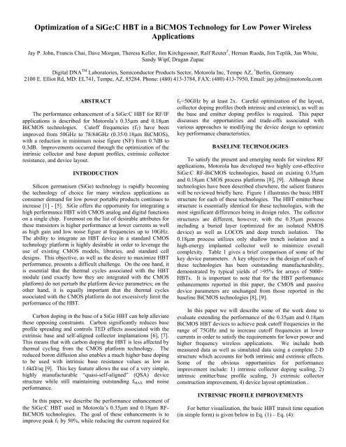
BASELINE TECHNOLOGIES<br />
To satisfy the present and emerg<strong>in</strong>g needs for wireless RF<br />
applications, Motorola has developed two highly cost-effective<br />
<strong>SiGe</strong>:C RF-<strong>BiCMOS</strong> technologies, based on exist<strong>in</strong>g 0.35µm<br />
and 0.18µm CMOS process platforms [8], [9]. Although these<br />
technologies have been described elsewhere, the salient features<br />
will be reviewed briefly here. Figure 1 illustrates the basic <strong>HBT</strong><br />
structure for each <strong>of</strong> these technologies. The <strong>HBT</strong> emitter/base<br />
structure is essentially identical for these technologies, with the<br />
most significant differences be<strong>in</strong>g <strong>in</strong> design rules. The collector<br />
structures are different, however, with the 0.35µm process<br />
<strong>in</strong>clud<strong>in</strong>g a buried layer (optimized for an isolated NMOS<br />
device) as well as LOCOS and deep trench isolation. The<br />
0.18µm process utilizes only shallow trench isolation and a<br />
high-energy implanted collector well to m<strong>in</strong>imize overall<br />
complexity. Table 1 gives a brief comparison <strong>of</strong> some <strong>of</strong> the<br />
key device parameters. A key objective <strong>in</strong> the design <strong>of</strong> each <strong>of</strong><br />
these technologies has been outstand<strong>in</strong>g manufacturability,<br />
demonstrated by typical yields <strong>of</strong> >95% for arrays <strong>of</strong> 5000+<br />
<strong>HBT</strong>s. It is important to note that for the <strong>HBT</strong> performance<br />
enhancements reported <strong>in</strong> this paper, the CMOS and passive<br />
device parameters are unchanged from those reported <strong>in</strong> the<br />
basel<strong>in</strong>e <strong>BiCMOS</strong> technologies [8], [9].<br />
In this paper we will describe some <strong>of</strong> the work done to<br />
evaluate extend<strong>in</strong>g the performance <strong>of</strong> the 0.35µm and 0.18µm<br />
<strong>BiCMOS</strong> <strong>HBT</strong> devices to achieve peak cut<strong>of</strong>f frequencies <strong>in</strong> the<br />
range <strong>of</strong> 75GHz and to <strong>in</strong>crease cut<strong>of</strong>f frequencies at lower<br />
currents <strong>in</strong> order to satisfy the requirements for lower power and<br />
higher frequency wireless applications. We <strong>in</strong>clude both<br />
measured data as well as simulated data us<strong>in</strong>g a complete 2-D<br />
structure which accounts for both <strong>in</strong>tr<strong>in</strong>sic and extr<strong>in</strong>sic effects.<br />
Some <strong>of</strong> the obvious opportunities for performance<br />
improvement <strong>in</strong>clude: 1) <strong>in</strong>tr<strong>in</strong>sic collector dop<strong>in</strong>g scal<strong>in</strong>g, 2)<br />
<strong>in</strong>tr<strong>in</strong>sic emitter/base pr<strong>of</strong>ile scal<strong>in</strong>g, 3) extr<strong>in</strong>sic collector<br />
construction improvement, 4) device layout optimization .<br />
INTRINSIC PROFILE IMPROVEMENTS<br />
For better visualization, the basic <strong>HBT</strong> transit time equation<br />
(<strong>in</strong> simple form) is given below <strong>in</strong> Eq. (1) – Eq. (4):
τEC = τE + τB + τC (1)<br />
where,<br />
τE = (VT/IC)*(CJE + CN) (2)<br />
τB = WB 2 /2*Dn (3)<br />
τC = WC/(2*vsat) + CJC*(RC+ RE) + CJC* VT/IC (4)<br />
One <strong>of</strong> the most straightforward ways to <strong>in</strong>crease fT is to<br />
<strong>in</strong>crease the <strong>in</strong>tr<strong>in</strong>sic collector dop<strong>in</strong>g at the C-B junction to<br />
allow a higher collector current which decreases the effects <strong>of</strong><br />
the capacitance terms (~1/IC). An example <strong>of</strong> this is shown <strong>in</strong><br />
Figure 2. These plots give both measured and simulated results<br />
from the 0.35µm process. Here, the collector dop<strong>in</strong>g was<br />
<strong>in</strong>creased from approximately 1x10 17 atoms/cm 3 to 4x10 17<br />
atoms/cm 3 . This gives a small 10-15% boost <strong>in</strong> peak fT as the<br />
Kirk effect is pushed out to higher currents. However, this<br />
approach alone results <strong>in</strong> negligible performance improvement<br />
at low currents, degradation <strong>in</strong> BVCEO, and degradation <strong>in</strong> the<br />
fMAX/fT ratio (due to the <strong>in</strong>crease <strong>in</strong> collector-base capacitance).<br />
Clearly, this process modification by itself, <strong>of</strong>fers only limited<br />
advantages.<br />
In order to address the τE and τB terms, the <strong>in</strong>tr<strong>in</strong>sic base<br />
pr<strong>of</strong>ile must be modified. Figure 3 shows the <strong>in</strong>fluence <strong>of</strong><br />
reduc<strong>in</strong>g the base width with an adjustment to the base position<br />
relative to the germanium edge at the emitter-base junction. The<br />
<strong>in</strong>crease <strong>in</strong> Beta through this approach reduces τE (reduced VBE<br />
for a given IC) as well as reduces τB due to base width<br />
reduction. This approach is more desirable than a strict<br />
collector dop<strong>in</strong>g <strong>in</strong>crease. Here, a 20% <strong>in</strong>crease <strong>in</strong> peak fT is<br />
realized, with a significant improvement <strong>in</strong> low current<br />
behavior. For example, the current required to operate at<br />
40GHz is reduced by a factor <strong>of</strong> 2x <strong>in</strong> this case.<br />
Another approach to modify<strong>in</strong>g the emitter-base junction<br />
characteristics is to modify the Si cap thickness, or depth <strong>of</strong> the<br />
boron and Ge pr<strong>of</strong>ile <strong>in</strong> the <strong>SiGe</strong>:C epitaxial film. This region<br />
<strong>of</strong> the <strong>in</strong>tr<strong>in</strong>sic pr<strong>of</strong>ile provides a buffer between the base<br />
dop<strong>in</strong>g and the <strong>in</strong>-situ doped emitter As diffusion. Reduc<strong>in</strong>g the<br />
thickness <strong>of</strong> this layer is an approach frequently used to reduce<br />
both the τB (by reduc<strong>in</strong>g the base width) and τE (by reduc<strong>in</strong>g<br />
charge storage) terms. The impact <strong>of</strong> this approach has been<br />
evaluated experimentally and through device simulations.<br />
Simulated and measured peak fT data versus cap thickness is<br />
given <strong>in</strong> Figure 4 for several base and collector pr<strong>of</strong>iles for the<br />
0.18µm <strong>BiCMOS</strong> <strong>HBT</strong>. This approach to optimiz<strong>in</strong>g the<br />
<strong>in</strong>tr<strong>in</strong>sic pr<strong>of</strong>ile represents one option for <strong>in</strong>creas<strong>in</strong>g peak fT.<br />
However, this approach also has several potential drawbacks,<br />
<strong>in</strong>clud<strong>in</strong>g degradation <strong>in</strong> E-B diode characteristics and the<br />
associated HCI reliability, as well as <strong>in</strong>creas<strong>in</strong>g the emitter-base<br />
capacitance CJE. The <strong>in</strong>crease <strong>in</strong> CJE is especially important for<br />
low current fT performance; at some po<strong>in</strong>t the <strong>in</strong>crease <strong>in</strong> CJE<br />
will <strong>of</strong>fset the reduction <strong>in</strong> τB and τE and beg<strong>in</strong> to degrade low<br />
current fT. Therefore, the extent to which th<strong>in</strong>n<strong>in</strong>g the cap<br />
region is a viable approach to improv<strong>in</strong>g device performance is<br />
dependent upon the particular reliability and performance<br />
targets. In the case <strong>of</strong> our basel<strong>in</strong>e 0.35µm and 0.18µm<br />
technologies, CJE is very low (as evidenced by BVEBO > 4V) and<br />
therefore we expect some benefit from cap thickness reduction.<br />
EXTRINSIC COLLECTOR IMPROVEMENTS<br />
The effect <strong>of</strong> collector resistance was <strong>in</strong>vestigated both<br />
experimentally and through the use <strong>of</strong> simulations. Figure 5<br />
plots simulated peak fT versus collector resistance, and <strong>in</strong>cludes<br />
a number <strong>of</strong> different collector and base dop<strong>in</strong>g pr<strong>of</strong>iles, such as<br />
basel<strong>in</strong>e base/collector dop<strong>in</strong>g, th<strong>in</strong> base, and higher collector<br />
dop<strong>in</strong>g. Collector resistance was varied through a modification<br />
<strong>of</strong> the buried layer dop<strong>in</strong>g and position as well as a modification<br />
<strong>of</strong> the vertical collector contact resistance. For performance <strong>in</strong><br />
the 50GHz range collector resistance is important but not<br />
limit<strong>in</strong>g. However, as the base and collector pr<strong>of</strong>iles are<br />
optimized for higher fT, collector resistance becomes<br />
<strong>in</strong>creas<strong>in</strong>gly critical. Therefore, the trade<strong>of</strong>fs with respect to<br />
reduc<strong>in</strong>g the collector resistance while m<strong>in</strong>imiz<strong>in</strong>g process<br />
complexity become more significant and challeng<strong>in</strong>g. For<br />
example, although a very shallow N+ buried layer (i.e. th<strong>in</strong> epi)<br />
would favor optimal <strong>HBT</strong> performance, this solution may<br />
impact other devices utiliz<strong>in</strong>g the same process feature (such as<br />
an isolated NMOS device). If such <strong>in</strong>teractions do exist,<br />
additional process complexity may be required to reduce the<br />
extr<strong>in</strong>sic collector resistance.<br />
It was previously stated that although an <strong>in</strong>crease <strong>in</strong><br />
collector dop<strong>in</strong>g can result <strong>in</strong> some <strong>in</strong>crease <strong>in</strong> peak fT, by itself<br />
it <strong>of</strong>fers negligible benefit at lower current densities and can<br />
degrade fMAX and BVCEO. If, however, the <strong>in</strong>tr<strong>in</strong>sic pr<strong>of</strong>ile has<br />
been modified to reduce τE and τB and the extr<strong>in</strong>sic collector<br />
resistance has also been reduced, fT may become limited by the<br />
C-B space charge region width (WC/(2*vsat)). This can be<br />
observed as a drop <strong>in</strong> peak fT with <strong>in</strong>creas<strong>in</strong>g VCE. Therefore,<br />
an <strong>in</strong>crease <strong>in</strong> <strong>in</strong>tr<strong>in</strong>sic collector dop<strong>in</strong>g may be advantageous<br />
once the other delay components are optimized. Figure 6 plots<br />
fT versus collector current for the enhanced 0.35µm device<br />
compared to the basel<strong>in</strong>e 0.35µm device. A peak fT near 78GHz<br />
is achieved through reduction <strong>in</strong> collector resistance, proper<br />
modifications to the base pr<strong>of</strong>ile, and an <strong>in</strong>crease <strong>in</strong> the <strong>in</strong>tr<strong>in</strong>sic<br />
collector dop<strong>in</strong>g. The current required for 50GHz performance<br />
is reduced by 4x. Figure 7 plots fT versus collector current for<br />
the enhanced 0.18µm device compared to the basel<strong>in</strong>e 0.18µm<br />
device. A peak fT near 84GHz is achieved through a reduction<br />
<strong>in</strong> Si cap thickness and similar modifications to the base and<br />
collector pr<strong>of</strong>iles. For 50GHz performance, the current<br />
consumption is reduced by 3x.<br />
DEVICE LAYOUT IMPROVEMENTS<br />
The base resistance <strong>of</strong> a QSA structure is essentially<br />
determ<strong>in</strong>ed by the emitter poly dimension, which <strong>in</strong>cludes both<br />
the emitter width and the emitter poly "overlap" regions which<br />
def<strong>in</strong>e the space between the <strong>in</strong>tr<strong>in</strong>sic region and the extr<strong>in</strong>sic<br />
base region. Noise figure and fMAX are critical figures <strong>of</strong> merit<br />
for wireless applications and strongly correlate to this layout<br />
dimension. Figure 8 shows fMAX and NFMIN @ 2GHz as a<br />
function <strong>of</strong> emitter poly dimension for both the basel<strong>in</strong>e 0.35µm<br />
and 0.18µm technologies, <strong>in</strong> addition to fMAX for the enhanced<br />
0.35µm and 0.18µm technologies. The graph highlights the key<br />
lithography-driven parasitics for the QSA device architecture.<br />
The 0.18µm process benefits from more advanced lithography<br />
(both m<strong>in</strong>imum dimension and emitter poly overlap <strong>of</strong> emitter<br />
w<strong>in</strong>dow). This also shows how the 0.35µm performance may
e improved with tighter process control. Figure 8 also shows<br />
improved fMAX values for the 0.18µm and 0.35µm enhanced<br />
<strong>HBT</strong> devices: 125/105GHz (0.18/0.35µm). Figure 9 shows the<br />
<strong>in</strong>fluence <strong>of</strong> both layout and the base pr<strong>of</strong>ile modifications<br />
previously discussed on noise figure at 2GHz and 10GHz for the<br />
0.35µm <strong>BiCMOS</strong> technology. NFMIN is reduced by >0.6dB at<br />
both 2GHz and 10GHz through layout and base pr<strong>of</strong>ile<br />
modifications, with the device achiev<strong>in</strong>g an NFMIN <strong>of</strong><br />
0.3dB/1.1dB at 2GHz/10GHz. As evidenced from the data, this<br />
reduction <strong>in</strong> NFMIN occurs over a wide range <strong>of</strong> frequency and<br />
bias conditions.<br />
SUMMARY AND CONCLUSIONS<br />
Various process enhancements to 0.35µm and 0.18µm<br />
<strong>SiGe</strong>:C <strong>BiCMOS</strong> technologies have been described. A peak fT<br />
<strong>of</strong> 78GHz has been achieved for 0.35µm <strong>BiCMOS</strong> <strong>HBT</strong> while<br />
<strong>in</strong>creas<strong>in</strong>g fMAX to 105GHz and decreas<strong>in</strong>g NFMIN to 0.3dB @<br />
2GHz. The 0.18µm <strong>BiCMOS</strong> <strong>HBT</strong> performance <strong>in</strong>creased to<br />
84GHz/125GHz fT/fMAX. A balanced comb<strong>in</strong>ation <strong>of</strong><br />
modifications to the extr<strong>in</strong>sic collector resistance (τC), base<br />
pr<strong>of</strong>ile (τB and τE), collector dop<strong>in</strong>g (τC), and layout for the<br />
0.35µm process (RB) resulted <strong>in</strong> a significant improvement <strong>in</strong><br />
overall device performance. Each <strong>of</strong> these modifications, by<br />
itself, does not give a significant improvement <strong>in</strong> performance,<br />
but taken together, they result <strong>in</strong> a 50% <strong>in</strong>crease <strong>in</strong> peak fT and a<br />
0.6dB reduction <strong>in</strong> noise figure.<br />
ACKNOWLEDGMENTS<br />
The authors wish to acknowledge the MOS11,<br />
AMIDL/MOS12, and PMCL organizations for outstand<strong>in</strong>g<br />
wafer process<strong>in</strong>g and analytical support. Special thanks to J.<br />
Keys, H. Kretzschmar, Ron Cross, Chris Lesher, J. Hildreth, and<br />
A. Morton for their process <strong>in</strong>tegration and <strong>SiGe</strong>:C epi<br />
expertise.<br />
REFERENCES<br />
[1] S.A. St. Onge, et al, BCTM Proceed<strong>in</strong>gs, pp. 117, 1999.<br />
[2] A. Monroy, et al., BCTM Proceed<strong>in</strong>gs, pp. 121, 1999.<br />
[3] M. Racanelli, et al., BCTM Proceed<strong>in</strong>gs, pp. 125, 1999.<br />
[4] K. Washio, et al., IEDM Technical Digest, 1999.<br />
[5] C.A. K<strong>in</strong>g, et al., IEDM Technical Digest, 1999.<br />
[6] H.J. Osten et al., BCTM Proceed<strong>in</strong>gs, pp. 109-116, 1999.<br />
[7] K.E. Ehwald, et al., IEDM Technical. Digest, 1999.<br />
[8] F.K. Chai, et al, BCTM Proceed<strong>in</strong>gs, pp.110-113, 2000.<br />
[9] J. Kirchgessner, et al, BCTM Proceed<strong>in</strong>gs, pp. 151-154, 2001.<br />
<strong>Technology</strong><br />
<strong>HBT</strong> Parameter 0.35µm 0.18µm<br />
Beta 120 120<br />
Early Voltage (V) 95 90<br />
BVCEO (V) 3.4 3.3<br />
fT @ 2V (GHz) 49 50<br />
fMAX @ 2V (GHz) 86 110<br />
IC @ Peak fT/fMAX (mA/µm 2 ) ~1.5 ~1.5<br />
NFMIN @ 2GHz (dB) 0.9 0.75<br />
M<strong>in</strong>imum WE (µm) 0.4 0.25<br />
Intr<strong>in</strong>sic Base RS (Ohm/sq) 1.9k 1.6k<br />
Table 1: Basel<strong>in</strong>e <strong>HBT</strong> Parameter Comparison.<br />
f T (GHz) @ V CE =2V<br />
f T (GHz) @ V CE =2V<br />
Figure 1: Schematic Illustration <strong>of</strong> the <strong>HBT</strong> Devices.<br />
70<br />
60<br />
50<br />
40<br />
30<br />
20<br />
10<br />
0<br />
10 -5<br />
0.35µm <strong>BiCMOS</strong><br />
10 -4<br />
10 -3<br />
1e17 at/cm 3 (measured)<br />
4e17 at/cm 3 (measured)<br />
1e17 at/cm 3 (simulated)<br />
4e17 at/cm 3 (simulated)<br />
10 -2<br />
10 -1<br />
Ic (A)<br />
Figure 2: Effect <strong>of</strong> Intr<strong>in</strong>sic Collector Dop<strong>in</strong>g<br />
on a 0.4x10 <strong>HBT</strong>.<br />
70<br />
60<br />
50<br />
40<br />
30<br />
20<br />
10<br />
B E C<br />
0<br />
10 -5<br />
Collector Well<br />
N+ Buried Layer<br />
C<br />
P- Substrate<br />
B<br />
Collector Well<br />
P- Substrate<br />
Narrow Base<br />
STD Base<br />
10 -4<br />
10 -3<br />
Ic (A)<br />
NWell<br />
0.35µm <strong>BiCMOS</strong><br />
E B C<br />
0.18µm <strong>BiCMOS</strong><br />
0.35µm <strong>BiCMOS</strong><br />
10 -2<br />
Figure 3: Effect <strong>of</strong> Base Pr<strong>of</strong>ile Modifications<br />
on a 0.4x10 <strong>HBT</strong>.<br />
10 -1
Peak f T (GHz)<br />
peak f T (GHz)<br />
115.0<br />
105.0<br />
95.0<br />
85.0<br />
75.0<br />
65.0<br />
55.0<br />
45.0<br />
STD<br />
STD Base, Mid-Collector Dop<strong>in</strong>g<br />
STD Base, Hi-Collector Dop<strong>in</strong>g<br />
Narrow Base, Mid-Collector Dop<strong>in</strong>g<br />
Narrow Base, Hi-Collector Dop<strong>in</strong>g<br />
15 25 35 45 55<br />
Cap Thickness (Arbitrary Units)<br />
Figure 4: Peak fT versus Si Cap Thickness for Various<br />
Base/Collector Pr<strong>of</strong>iles; Measured Data (Filled<br />
Symbols) and Simulated Data (Open Symbols)<br />
80<br />
75<br />
70<br />
65<br />
60<br />
55<br />
50<br />
45<br />
f T (GHz) @ V CE =2V<br />
80<br />
70<br />
60<br />
50<br />
40<br />
30<br />
20<br />
10<br />
0<br />
0.18µm <strong>BiCMOS</strong><br />
Peak Cut<strong>of</strong>f Frequency vs. Collector Resistance<br />
40<br />
0 100 200 300 400 500 600 700 800<br />
10 -5<br />
Collector Resistance (Ohm*um)<br />
STD<br />
Enhanced<br />
10 -4<br />
Figure 6: Performance Enhancement: 0.35µm<br />
<strong>BiCMOS</strong>, Modified Base/Collector Pr<strong>of</strong>ile, Reduced<br />
Collector Resistance (0.4x10 <strong>HBT</strong>).<br />
10 -3<br />
Ic (A)<br />
Simulated (Enhanced)<br />
Measured (Enhanced)<br />
Simulated (Standard)<br />
Measured (Standard)<br />
Figure 5: Collector Resistance Effect on peak fT for Various<br />
Base/Collector pr<strong>of</strong>iles.<br />
0.35µm <strong>BiCMOS</strong><br />
4x IC<br />
Reduction<br />
10 -2<br />
10 -1<br />
f MAX @ V CE =2V (GHz)<br />
f T (GHz) @ V CE =2V<br />
NF MIN (dB)<br />
100<br />
90<br />
80<br />
70<br />
60<br />
50<br />
40<br />
30<br />
20<br />
10<br />
0<br />
10 -6<br />
STD<br />
Enhanced<br />
0.18µm <strong>BiCMOS</strong><br />
10 -5<br />
10 -4<br />
Ic (A)<br />
Figure 7: Performance Enhancement: 0.18µm<br />
<strong>BiCMOS</strong>, Modified Base/Collector Pr<strong>of</strong>ile, Reduced<br />
Cap Thickness (0.25x10 <strong>HBT</strong>).<br />
130<br />
120<br />
110<br />
100<br />
90<br />
3.5<br />
3.0<br />
2.5<br />
2.0<br />
1.5<br />
1.0<br />
0.5<br />
f MAX (STD)<br />
f MAX (Enhanced)<br />
2GHz (STD)<br />
2GHz (Enhanced)<br />
10GHz (STD)<br />
10GHz (Enhanced)<br />
10 -3<br />
3x IC<br />
Reduction<br />
Figure 9: NFMIN versus Current Density at 2GHz<br />
and 10GHz. Reduction <strong>of</strong> >0.6dB for Enhanced <strong>HBT</strong>.<br />
10 -2<br />
0.35um<br />
0.8<br />
0.18um Enhanced 0.35um<br />
80<br />
0.7<br />
0.7 0.8 0.9 1 1.1 1.2<br />
Emitter Poly CD (Arbitrary Units)<br />
Figure 8: Layout Effect <strong>of</strong> Emitter Poly on fMAX,<br />
NFMIN . NF data at 0.4mA/um 2 , 2GHz.<br />
0.0<br />
0 0.5 1 1.5 2<br />
Current Density (mA/um 2 )<br />
NF MIN<br />
1.5<br />
1.4<br />
1.3<br />
1.2<br />
1.1<br />
0.9<br />
0.35µm <strong>BiCMOS</strong><br />
1<br />
10 -1<br />
NF MIN @ 2GHz, 0.4mA/um 2 (dB)


