

AN1097 Calibration-Free Pressure Sensor System - Freescale
AN1097 Calibration-Free Pressure Sensor System - Freescale
AN1097 Calibration-Free Pressure Sensor System - Freescale

Create successful ePaper yourself
Turn your PDF publications into a flip-book with our unique Google optimized e-Paper software.
<strong>Free</strong>scale Semiconductor<br />
Application Note<br />
© <strong>Free</strong>scale Semiconductor, Inc., 2005. All rights reserved.<br />
<strong>AN1097</strong><br />
Rev 3, 05/2005<br />
<strong>Calibration</strong>-<strong>Free</strong> <strong>Pressure</strong> <strong>Sensor</strong> <strong>System</strong><br />
by: Michel Burri, Senior <strong>System</strong> Engineer<br />
Geneva, Switzerland<br />
INTRODUCTION<br />
The MPX2000 series pressure transducers are<br />
semiconductor devices which give an electrical output signal<br />
proportional to the applied pressure. The sensors are a single<br />
monolithic silicon diaphragm with strain gauge and thin-film<br />
resistor networks on the chip. Each chip is laser trimmed for<br />
full scale output, offset, and temperature compensation.<br />
The purpose of this document is to describe another<br />
method of measurement which should facilitate the life of the<br />
design. The MPX2000 series sensors are available both as<br />
unported elements and as ported assemblies suitable for<br />
pressure, vacuum and differential pressure measurements in<br />
the range of 10 kPa through 200 kPa.<br />
The use of the on-chip A/D converter of the MC68HC05B6<br />
HCMOS MCU makes possible the design of an accurate and<br />
reliable pressure measurement system.<br />
SYSTEM ANALYSIS<br />
The measurement system is made up of the pressure<br />
sensor, the amplifiers, and the MCU. Each element in the<br />
chain has its own device-to-device variations and temperature<br />
effects which should be analyzed separately. For instance, the<br />
8-bit A/D converter has a quantization error of about ±0.2<br />
percent. This error should be subtracted from the maximum<br />
error specified for the system to find the available error for the<br />
rest of elements in the chain. The MPX2000 series pressure<br />
sensors are designed to provide an output sensitivity of 4.0<br />
mV/V excitation voltage with full-scale pressure applied or 20<br />
mV at the excitation voltage of 5.0 V DC.<br />
An interesting property must be considered to define the<br />
configuration of the system: the ratiometric function of both the<br />
A/D converter and the pressure sensor device. The ratiometric<br />
function of these elements makes all voltage variations from<br />
the power supply rejected by the system. With this advantage,<br />
it is possible to design a chain of amplification where the signal<br />
is conditioned in a different way.<br />
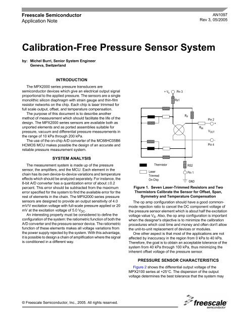
Laser<br />
Trimmed<br />
On-Chip<br />
+ V s<br />
Thermistor<br />
Pin 3<br />
Rs1<br />
Figure 1. Seven Laser-Trimmed Resistors and Two<br />
Thermistors Calibrate the <strong>Sensor</strong> for Offset, Span,<br />
Symmetry and Temperature Compensation<br />
The op amp configuration should have a good commonmode<br />
rejection ratio to cancel the DC component voltage of<br />
the pressure sensor element which is about half the excitation<br />
voltage value VS . Also, the op amp configuration is important<br />
when the designer's objective is to minimize the calibration<br />
procedures which cost time and money and often don't allow<br />
the unit-to-unit replacement of devices or modules.<br />
One other aspect is that most of the applications are not<br />
affected by inaccuracy in the region from 0 kPa to 40 kPa.<br />
Therefore, the goal is to obtain an acceptable tolerance of the<br />
system from 40 kPa through 100 kPa, thus minimizing the<br />
inherent offset voltage of the pressure sensor.<br />
PRESSURE SENSOR CHARACTERISTICS<br />
Figure 2 shows the differential output voltage of the<br />
MPX2100 series at +25°C. The dispersion of the output<br />
voltage determines the best tolerance that the system may<br />
R P<br />
RS2<br />
Pin 1<br />
GND<br />
R IN<br />
Pin 2<br />
+<br />
V OUT<br />
-<br />
Pin 4
achieve without undertaking a calibration procedure, if any<br />
other elements or parameters in the chain do not introduce<br />
additional errors.<br />
V OUT (mV)<br />
20<br />
10<br />
5<br />
0<br />
-5<br />
Figure 2. Spread of the Output Voltage versus the<br />
Applied <strong>Pressure</strong> at 25°C<br />
The effects of temperature on the full scale output and<br />
offset are shown in Figure 3. It is interesting to notice that the<br />
offset variation is greater than the full scale output and both<br />
have a positive temperature coefficient respectively of +8.0<br />
µV/degree and +5.0 µV excitation voltage. That means that<br />
the full scale variation may be compensated by modifying the<br />
gain somewhere in the chain amplifier by components<br />
arranged to produce a negative TC of 250 PPM/°C. The dark<br />
area of Figure 3 shows the trend of the compensation which<br />
improves the full scale value over the temperature range. In<br />
the area of 40 kPa, the compensation acts in the ratio of<br />
40/100 of the value of the offset temperature coefficient.<br />
Figure 3. Output Voltage versus Temperature. The Dark<br />
Area Shows the Trend of the Compensation<br />
<strong>AN1097</strong><br />
V S =5<br />
V DCT A =25°C<br />
0 20 40 60 80 100<br />
V OUT (f) ∆T<br />
+85°C<br />
Offset Variation<br />
-15°C<br />
OFFSET<br />
0 20 40 60 80 100<br />
Positive<br />
Full Scale<br />
Variation<br />
OP AMP CHARACTERISTICS<br />
FULL-SCALE<br />
P<br />
(kPa)<br />
P<br />
(kPa)<br />
For systems with only one power supply, the instrument<br />
amplifier configuration shown in Figure 4 is a good solution to<br />
monitor the output of a resistive transducer bridge.<br />
The instrument amplifier does provide an excellent CMRR<br />
and a symmetrical buffered high input impedance at both noninverting<br />
and inverting terminals. It minimizes the number of<br />
the external passive components used to set the gain of the<br />
amplifier. Also, it is easy to compensate the temperature<br />
variation of the Full Scale Output of the <strong>Pressure</strong> <strong>Sensor</strong> by<br />
implementing resistors “R f” having a negative coefficient<br />
temperature of -250 PPM/°C.<br />
The differential-mode voltage gain of the instrument<br />
amplifier is:<br />
Figure 4. One Power Supply to Excite the Bridge and to<br />
Develop a Differential Output Voltage<br />
The major source of errors introduced by the op amp is<br />
offset voltages which may be positive or negative, and the<br />
input bias current which develops a drop voltage ∆V through<br />
the feedback resistance Rf. When the op amp input is<br />
composed of PNP transistors, the whole characteristic of the<br />
transfer function is shifted below the DC component voltage<br />
value set by the <strong>Pressure</strong> <strong>Sensor</strong> as shown in Figure 5.<br />
The gain of the instrument amplifier is calculated carefully<br />
to avoid a saturation of the output voltage, and to provide the<br />
maximum of differential output voltage available for the A/D<br />
Converter. The maximum output swing voltage of the<br />
amplifiers is also dependent on the bias current which creates<br />
a ∆V voltage on the feedback resistance Rf and on the Full<br />
Scale output voltage of the pressure sensor.<br />
<strong>Sensor</strong>s<br />
2 <strong>Free</strong>scale Semiconductor<br />
3<br />
4<br />
Avd =<br />
V1-V2<br />
Vs2-Vs4 = 1 + 2 R f<br />
R g<br />
2<br />
1<br />
R G<br />
+<br />
-<br />
-<br />
+<br />
R f<br />
+V S<br />
V1<br />
V2<br />
0 V<br />
(1)
Figure 5. Instrument Amplifier Transfer Function with<br />
Spread of the Device to Device Offset Variation<br />
Figure 5 shows the transfer function of different instrument<br />
amplifiers used in the same application. The same sort of<br />
random errors are generated by crossing the inputs of the<br />
instrument amplifier. The spread of the differential output<br />
voltage (V1-V2) and (V2x-V1x) is due to the unsigned voltage<br />
offset and its absolute value. Figure 6 and Figure 7 show the<br />
unit-to-unit variations of both the offset and the bias current of<br />
the dual op amp MC33078.<br />
+2<br />
+1<br />
V CC<br />
1/2<br />
V CC<br />
V EE<br />
V io (mV)<br />
0<br />
-1<br />
-2<br />
V1, V2<br />
5 V DC<br />
V2<br />
Figure 6. Input Offset Voltage versus Temperature<br />
To realize such a system, the designer must provide a<br />
calibration procedure which is very time consuming. Some<br />
extra potentiometers must be implemented for setting both the<br />
offset and the Full Scale Output with a complex temperature<br />
compensation network circuit.<br />
The new proposed solution will reduce or eliminate any<br />
calibration procedure.<br />
V1<br />
V2X<br />
V1X<br />
0 5 10 15 20<br />
UNIT 1<br />
UNIT 2<br />
UNIT 3<br />
-50 -25 0 25 50 75 100 125<br />
VPS<br />
(mV)<br />
T<br />
(°C)<br />
Figure 7. Input Bias Current versus Temperature<br />
MCU CONTRIBUTION<br />
As shown in Figure 5, crossing the instrument amplifier<br />
inputs generated their mutual differences which can be<br />
computed by the MCU.<br />
Figure 8. Crossing of the Instrument Amplifier Input<br />
Using a Port of the MCU<br />
Figure 8 shows the analog switches on the front of the<br />
instrument amplifier and the total symmetry of the chain. The<br />
residual resistance RDS(on) of the switches does not introduce<br />
errors due to the high input impedance of the instrument<br />
amplifier.<br />
With the aid of two analog switches, the MCU successively<br />
converts the output signals V1, V2.<br />
Four conversions are necessary to compute the final result.<br />
First, two conversions of V1 and V2 are executed and stored<br />
in the registers R1, R2. Then, the analog switches are<br />
commuted in the opposite position and the two last<br />
conversions of V2x and V1x are executed and stored in the<br />
registers R2x and R1x. Then, the MCU computes the following<br />
equation:<br />
<strong>AN1097</strong><br />
<strong>Sensor</strong>s<br />
<strong>Free</strong>scale Semiconductor 3<br />
3<br />
4<br />
600<br />
450<br />
300<br />
150<br />
0<br />
l ib (nA)<br />
UNIT 1<br />
UNIT 2<br />
-50 -25 0 25 50 75 100 125<br />
2<br />
1<br />
R g<br />
-<br />
+<br />
+<br />
-<br />
R f<br />
+V S<br />
T<br />
(°C)<br />
V1<br />
V2<br />
P<br />
0 V
RESULT = (R1-R2) + (R2x-R1x) (2)<br />
The result is twice a differential conversion. As<br />
demonstrated below, all errors from the instrument amplifier<br />
<strong>Pressure</strong><br />
<strong>Sensor</strong><br />
<strong>System</strong><br />
<strong>AN1097</strong><br />
3<br />
4<br />
MPX2100AP<br />
are cancelled. Other averaging techniques may be used to<br />
improve the result, but the appropriated algorithm is always<br />
determined by the maximum bandwidth of the input signal and<br />
the required accuracy of the system.<br />
Figure 9. Two Channel Input and One Output Port Are Used by the MCU<br />
SYSTEM CALCULATION<br />
There is a full cancellation of the amplifier offset OF1 and<br />
OF2. The addition of the two differential results V1-V2 and<br />
V2x-V1X produce a virtual output voltage VoutV which<br />
becomes the applied input voltage to the A/D converter. The<br />
result of the conversion is expressed in the number of counts<br />
or bits by the ratiometric formula shown below:<br />
2<br />
1<br />
MC74HC4053<br />
<strong>Sensor</strong> out 2 <strong>Sensor</strong> out 4<br />
Vs2 = a (P) + of2 Vs4 = b (P) + of4<br />
Amplifier out 1<br />
Amplifier out 2<br />
V1 = Avd (Vs2 + OF1) V2 = Avd (Vs4 + OF2)<br />
Inverting of the amplifier input<br />
V1x = Avd (Vs4 + OF1) V2x = Avd (Vs2 + OF2)<br />
Delta = V1-V2 1st differential result<br />
= Avd * (Vs2 of OF1) - Avd * (Vs4 + OF2)<br />
Deltax = V2x-V1x 2nd differential result<br />
= Avd * (Vs2 + OF2) - Vdc * (Vs4 + OF1)<br />
Adding of the two differential results<br />
VoutV = Delta + Deltax<br />
= Avd*Vs2 + Avd*OF2 + Avd*OF2 - Avd*OF1<br />
+ Avd*OF1 - Avd*OF2 + Avd*OF2 - Avd*OF1<br />
= 2 * Avd * (Vs2 -Vs4)<br />
= 2 * Avd * [(a (P) + of2) - (b (P) + of4)]<br />
= 2 * Avd * [V(P) + Voffset]<br />
count = VoutV *<br />
255<br />
VRH-VRL<br />
MC33078<br />
255 is the maximum number of counts provided by the A/D<br />
converter and VRH-VRL is the reference voltage of the<br />
ratiometric A/D converter which is commonly tied to the 5.0 V<br />
supply voltage of the MCU.<br />
When the tolerance of the full scale pressure has to be in<br />
the range of ± 2.5 percent, the offset of the pressure sensor<br />
may be neglected. That means the system does not require<br />
any calibration procedure.<br />
The equation of the system transfer is then:<br />
Avd is the differential-mode gain of the instrument amplifier<br />
which is calculated using the equation (1). Then with R f = 510<br />
kΩ and R g = 9.1 kΩ Avd = 113.<br />
The maximum counts available in the MCU register at the<br />
Full Scale <strong>Pressure</strong> is:<br />
knowing that the MPX2100AP pressure sensor provides 20mV<br />
at 5.0 excitation voltage and 100 kPa full scale pressure.<br />
The system resolution is 100 kPa/230 that give 0.43 kPa<br />
per count.<br />
<strong>Sensor</strong>s<br />
4 <strong>Free</strong>scale Semiconductor<br />
+<br />
+<br />
-<br />
-<br />
V1<br />
V2<br />
R f<br />
R g<br />
R f<br />
CH1<br />
MC68HC05B6<br />
P<br />
CH2<br />
count = 2 * Avd * V(P) * 51/V where:<br />
VRH V DD<br />
VRL V SS<br />
count (Full Scale) = 2 * 113 * 0.02 V * 51/V = 230<br />
+ 5 V<br />
I/O<br />
0 V
Figure 10. Full Scale Output <strong>Calibration</strong> Using the Reference Voltage VRH-VRL<br />
When the tolerance of the system has to be in the range of<br />
±1percent, the designer should provide only one calibration<br />
3<br />
4<br />
<strong>Pressure</strong><br />
<strong>Sensor</strong><br />
<strong>System</strong><br />
MPX2100AP<br />
2<br />
1<br />
FINE<br />
CAL.<br />
MC74HC4053<br />
procedure which sets the Full Scale Output (counts) at 25°C<br />
100 kPa or under the local atmospheric pressure conditions.<br />
Figure 11. One Channel Input and Two Output Ports are used by the MCU<br />
Due to the high impedance input of the A/D converter of the<br />
MC68HC05B6 MCU, another configuration may be<br />
implemented which uses only one channel input as shown in<br />
Figure 11. It is interesting to notice that practically any dual op<br />
amp may be used to do the job but a global consideration must<br />
be made to optimize the total cost of the system according to<br />
the requested specification.<br />
When the Full Scale <strong>Pressure</strong> has to be sent with accuracy,<br />
the calibration procedure may be executed in different ways.<br />
For instance, the module may be calibrated directly using<br />
Up/Down push buttons.<br />
The gain of the chain is set by changing the VRH voltage of<br />
the ratiometric A/D converter with the R/2R ladder network<br />
circuit which is directly driven by the ports of the MCU. (See<br />
Figure 12.)<br />
VRH<br />
CH1<br />
MC68HC05B6<br />
P<br />
CH2<br />
MC33078<br />
+<br />
-<br />
-<br />
+<br />
VRL V SS<br />
Using a communication bus, the calibration procedure may<br />
be executed from a host computer. In both cases, the setting<br />
value is stored in the EEPROM of the MCU.<br />
The gain may be also set using a potentiometer in place of<br />
the resistor R f. But, this component is expensive, taking into<br />
account that it must be stable over the temperature range at<br />
long term.<br />
<strong>AN1097</strong><br />
<strong>Sensor</strong>s<br />
<strong>Free</strong>scale Semiconductor 5<br />
V DD<br />
V1<br />
V2<br />
R f<br />
R g<br />
R f<br />
+ 5 V<br />
I/O<br />
0 V<br />
1/3<br />
MC74HC4053<br />
P1<br />
CH1<br />
P2<br />
VRH V DD<br />
MC68HC05B6<br />
VRL V SS<br />
+ 5 V<br />
I/O<br />
0 V
<strong>AN1097</strong><br />
Figure 12. R/2R Ladder Network for an MCU<br />
Table 1. <strong>Pressure</strong> Conversion Table<br />
Unity Pa mbar Torr atm at=kp/cm2 mWS psi<br />
1 N/m2 = 1 Pascal 1 0.01 7.5 10-3 - - - -<br />
1 mbar 100 1 0.75 - - 0.0102 0.014<br />
1 Torr = 1 mmHg 133.32 1.333 .1 - - - 0.019<br />
1 atm (1)<br />
101325 1013.2 760 1 1.033 10.33 14.69<br />
1 at = 1 kp/cm2 (2)<br />
98066.5 981 735.6 0.97 1 10 14.22<br />
1 m of water 9806.65 98.1 73.56 0.097 0.1 1 1.422<br />
1 lb/sqin = 1 psi 6894.8 68.95 51.71 0.068 - - 1<br />
NOTES:<br />
1. Normal atmosphere<br />
2. Technical atmosphere<br />
2R RO<br />
R/2R<br />
Ladder<br />
Network<br />
R<br />
R<br />
R<br />
2R<br />
2R<br />
2R<br />
2R<br />
VRH<br />
P3<br />
P2<br />
P1<br />
P0<br />
CH1<br />
CH2<br />
V DD<br />
MC68HC05B6<br />
VRL V SS<br />
<strong>Sensor</strong>s<br />
6 <strong>Free</strong>scale Semiconductor<br />
I/O<br />
+ 5.0 V<br />
BUS<br />
+ 5.0 V<br />
UP DOWN<br />
0 V
NOTES<br />
<strong>AN1097</strong><br />
<strong>Sensor</strong>s<br />
<strong>Free</strong>scale Semiconductor 7
How to Reach Us:<br />
Home Page:<br />
www.freescale.com<br />
E-mail:<br />
support@freescale.com<br />
USA/Europe or Locations Not Listed:<br />
<strong>Free</strong>scale Semiconductor<br />
Technical Information Center, CH370<br />
1300 N. Alma School Road<br />
Chandler, Arizona 85224<br />
+1-800-521-6274 or +1-480-768-2130<br />
support@freescale.com<br />
Europe, Middle East, and Africa:<br />
<strong>Free</strong>scale Halbleiter Deutschland GmbH<br />
Technical Information Center<br />
Schatzbogen 7<br />
81829 Muenchen, Germany<br />
+44 1296 380 456 (English)<br />
+46 8 52200080 (English)<br />
+49 89 92103 559 (German)<br />
+33 1 69 35 48 48 (French)<br />
support@freescale.com<br />
Japan:<br />
<strong>Free</strong>scale Semiconductor Japan Ltd.<br />
Headquarters<br />
ARCO Tower 15F<br />
1-8-1, Shimo-Meguro, Meguro-ku,<br />
Tokyo 153-0064<br />
Japan<br />
0120 191014 or +81 3 5437 9125<br />
support.japan@freescale.com<br />
Asia/Pacific:<br />
<strong>Free</strong>scale Semiconductor Hong Kong Ltd.<br />
Technical Information Center<br />
2 Dai King Street<br />
Tai Po Industrial Estate<br />
Tai Po, N.T., Hong Kong<br />
+800 2666 8080<br />
support.asia@freescale.com<br />
For Literature Requests Only:<br />
<strong>Free</strong>scale Semiconductor Literature Distribution Center<br />
P.O. Box 5405<br />
Denver, Colorado 80217<br />
1-800-441-2447 or 303-675-2140<br />
Fax: 303-675-2150<br />
LDCFor<strong>Free</strong>scaleSemiconductor@hibbertgroup.com<br />
<strong>AN1097</strong><br />
Rev 3<br />
05/2005<br />
Information in this document is provided solely to enable system and software<br />
implementers to use <strong>Free</strong>scale Semiconductor products. There are no express or<br />
implied copyright licenses granted hereunder to design or fabricate any integrated<br />
circuits or integrated circuits based on the information in this document.<br />
<strong>Free</strong>scale Semiconductor reserves the right to make changes without further notice to<br />
any products herein. <strong>Free</strong>scale Semiconductor makes no warranty, representation or<br />
guarantee regarding the suitability of its products for any particular purpose, nor does<br />
<strong>Free</strong>scale Semiconductor assume any liability arising out of the application or use of any<br />
product or circuit, and specifically disclaims any and all liability, including without<br />
limitation consequential or incidental damages. “Typical” parameters that may be<br />
provided in <strong>Free</strong>scale Semiconductor data sheets and/or specifications can and do vary<br />
in different applications and actual performance may vary over time. All operating<br />
parameters, including “Typicals”, must be validated for each customer application by<br />
customer’s technical experts. <strong>Free</strong>scale Semiconductor does not convey any license<br />
under its patent rights nor the rights of others. <strong>Free</strong>scale Semiconductor products are<br />
not designed, intended, or authorized for use as components in systems intended for<br />
surgical implant into the body, or other applications intended to support or sustain life,<br />
or for any other application in which the failure of the <strong>Free</strong>scale Semiconductor product<br />
could create a situation where personal injury or death may occur. Should Buyer<br />
purchase or use <strong>Free</strong>scale Semiconductor products for any such unintended or<br />
unauthorized application, Buyer shall indemnify and hold <strong>Free</strong>scale Semiconductor and<br />
its officers, employees, subsidiaries, affiliates, and distributors harmless against all<br />
claims, costs, damages, and expenses, and reasonable attorney fees arising out of,<br />
directly or indirectly, any claim of personal injury or death associated with such<br />
unintended or unauthorized use, even if such claim alleges that <strong>Free</strong>scale<br />
Semiconductor was negligent regarding the design or manufacture of the part.<br />
<strong>Free</strong>scale and the <strong>Free</strong>scale logo are trademarks of <strong>Free</strong>scale Semiconductor, Inc.<br />
All other product or service names are the property of their respective owners.<br />
© <strong>Free</strong>scale Semiconductor, Inc. 2005. All rights reserved.


