

MPC17511A - Freescale
MPC17511A - Freescale
MPC17511A - Freescale

Create successful ePaper yourself
Turn your PDF publications into a flip-book with our unique Google optimized e-Paper software.
<strong>Freescale</strong> Semiconductor<br />
Technical Data<br />
1.0 A 6.8 V H-Bridge Motor<br />
Driver IC<br />
The 17511A is a monolithic H-Bridge designed to be used in<br />
portable electronic applications to control small DC motors or bipolar<br />
step motors. End applications include head positioners (CDROM or<br />
disk drive), camera focus motors, and camera shutter solenoids.<br />
The 17511A can operate efficiently with supply voltages as low as<br />
2.0V to as high as 6.8V. Its low RDS(ON) H-Bridge output MOSFETs<br />
(0.46 Ω typical) can provide continuos motor drive currents of 1.0A<br />
and handle peak currents up to 3.0A. It is easily interfaced to low-cost<br />
MCUs via parallel 3.0V- or 5.0V- compatible logic. The device can be<br />
pulse width modulated (PWM-ed) at up to 200 kHz.<br />
This device contains an integrated charge pump and level shifter<br />
(for gate drive voltages), integrated shoot-through current protection<br />
(cross-conduction suppression logic and timing), and undervoltage<br />
detection and shutdown circuitry.<br />
The 17511A has four operating modes: Forward, Reverse, Brake,<br />
and Tri-Stated (High Impedance).<br />
Features<br />
• 2.0V to 6.8V Continuous Operation<br />
• Output Current 1.0 A(DC), 3.0A (Peak)<br />
• MOSFETs < 600 mΩ R DS(ON) @ 25°C Guaranteed<br />
• 3.0V/ 5.0V TTL- / CMOS-Compatible Inputs<br />
• PWM Frequencies up to 200 kHz<br />
• Undervoltage Shutdown<br />
• Cross-Conduction Suppression<br />
• Low Power Consumption<br />
• Pb-Free Packaging Designated by Suffix Codes EV and EP<br />
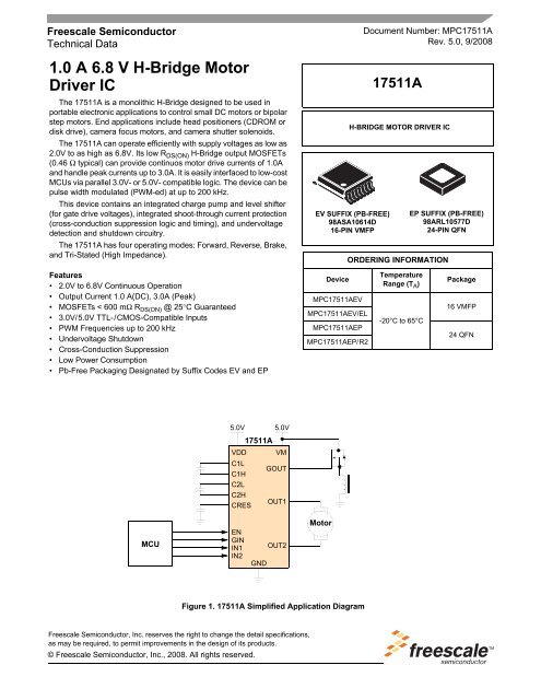
MCU<br />
5.0V<br />
5.0V<br />
17511A<br />
VDD VM<br />
C1L<br />
C1H<br />
C2L<br />
GOUT<br />
C2H<br />
CRES<br />
OUT1<br />
EN<br />
GIN<br />
IN1<br />
IN2<br />
GND<br />
OUT2<br />
Figure 1. 17511A Simplified Application Diagram<br />
<strong>Freescale</strong> Semiconductor, Inc. reserves the right to change the detail specifications,<br />
as may be required, to permit improvements in the design of its products.<br />
© <strong>Freescale</strong> Semiconductor, Inc., 2008. All rights reserved.<br />
Document Number: <strong>MPC17511A</strong><br />
Rev. 5.0, 9/2008<br />
H-BRIDGE MOTOR DRIVER IC<br />
EV SUFFIX (PB-FREE)<br />
98ASA10614D<br />
16-PIN VMFP<br />
Device<br />
<strong>MPC17511A</strong>EV<br />
<strong>MPC17511A</strong>EV/EL<br />
<strong>MPC17511A</strong>EP<br />
<strong>MPC17511A</strong>EP/ R2<br />
Motor<br />
17511A<br />
ORDERING INFORMATION<br />
Temperature<br />
Range (T A )<br />
-20°C to 65°C<br />
EP SUFFIX (PB-FREE)<br />
98ARL10577D<br />
24-PIN QFN<br />
Package<br />
16 VMFP<br />
24 QFN
INTERNAL BLOCK DIAGRAM<br />
17511A<br />
C2L<br />
C1H<br />
CRES<br />
VDD<br />
IN1<br />
IN2<br />
GIN<br />
EN<br />
V DD<br />
V DD<br />
Control<br />
Logic<br />
INTERNAL BLOCK DIAGRAM<br />
Low-<br />
Voltage<br />
Shutdown<br />
Charge Pump<br />
Level<br />
Shifter<br />
Predriver<br />
Figure 2. 17511A Simplified Internal Block Diagram<br />
Analog Integrated Circuit Device Data<br />
2 <strong>Freescale</strong> Semiconductor<br />
C2H<br />
C1L<br />
GOUT<br />
VM<br />
OUT1<br />
OUT2<br />
PGND<br />
LGND
C2L<br />
C1H<br />
C1L<br />
Table 1. VMFP Pin Function Description<br />
PIN CONNECTIONS<br />
Figure 3. VMFP Pin Connections<br />
Pin<br />
Number<br />
Pin Name Formal Name Definition<br />
1 C2L Charge Pump 2L Charge pump bucket capacitor 2 (negative pole).<br />
2 C1H Charge Pump 1H Charge pump bucket capacitor 1 (positive pole).<br />
3 C1L Charge Pump 1L Charge pump bucket capacitor 1 (negative pole).<br />
4 VM Motor Drive Power Supply Driver power supply voltage input pin.<br />
5 VDD Logic Supply Control circuit power supply pin.<br />
6 IN1 Input Control 1 Control signal input 1<br />
7 IN2 Input Control 2 Control signal input 2.<br />
8 EN Enable Control Enable control signal input pin.<br />
9 LGND Logic Ground Logic ground pin.<br />
10 GIN Gate Driver Input LOW = True control signal for GOUT pin.<br />
11 OUT1 H-Bridge Output 1 Driver output 1 (right half of H-Bridge).<br />
12 PGND Power Ground Driver ground pin.<br />
VM<br />
VDD<br />
IN1<br />
IN2<br />
EN<br />
13 OUT2 H-Bridge Output 2 Driver output 2 (left half of H-Bridge).<br />
14 GOUT Gate Driver Output Output gate driver signal to external MOSFET switch.<br />
15 CRES Charge Pump Output Capacitor<br />
Connection<br />
1<br />
2<br />
3<br />
4<br />
5<br />
6<br />
7<br />
8 9<br />
Charge pump reservoir capacitor pin.<br />
16 C2H Charge Pump 2H Charge pump bucket capacitor 2 (positive pole).<br />
PIN CONNECTIONS<br />
17511A<br />
Analog Integrated Circuit Device Data<br />
<strong>Freescale</strong> Semiconductor 3<br />
16<br />
15<br />
14<br />
13<br />
12<br />
11<br />
10<br />
C2H<br />
CRES<br />
GOUT<br />
OUT2<br />
PGND<br />
OUT1<br />
GIN<br />
LGND
PIN CONNECTIONS<br />
Table 2. QFN Pin Function Description<br />
17511A<br />
24<br />
1<br />
Figure 4. QFN Pin Connections<br />
Pin<br />
Number<br />
Pin Name Formal Name Definition<br />
1, 2, 3, 4 VM Motor Drive Power Supply Driver power supply voltage input pin.<br />
5, 6, 13, 18 NC No Connect This pin is not used.<br />
7 VDD Logic Supply Control circuit power supply pin.<br />
8 IN1 Logic Input Control 1 Control signal input 1.<br />
9 IN2 Logic Input Control 2 Control signal input 2.<br />
10 EN Enable Control Enable control signal input pin.<br />
11 LGND Logic Ground Logic ground pin.<br />
12 GIN Gate Driver Input LOW = True control signal for GOUT pin.<br />
14 OUT1 Output 1 Driver output 1 (right half of H-Bridge).<br />
15, 16 PGND Power Ground Driver ground pin.<br />
VM<br />
VM<br />
VM<br />
VM<br />
NC<br />
NC<br />
17 OUT2 Output 2 Driver output 2 (left half of H-Bridge).<br />
19 GOUT Gate Driver Output Output gate driver signal to external MOSFET switch.<br />
20 CRES Pre-Driver Power Supply Pre-driver circuit power supply pin.<br />
2<br />
3<br />
4<br />
5<br />
6<br />
7 8 9 10 11 12<br />
21 C2H Charge Pump 2H Charge pump bucket capacitor 2 (positive pole).<br />
22 C2L Charge Pump 2L Charge pump bucket capacitor 2 (negative pole).<br />
23 C1H Charge Pump 1H Charge pump bucket capacitor 1 (positive pole).<br />
24 C1L Charge Pump 1L Charge pump bucket capacitor 1 (negative pole).<br />
C1L<br />
VDD<br />
C1H<br />
23<br />
IN1<br />
C2L<br />
22<br />
IN2<br />
Analog Integrated Circuit Device Data<br />
4 <strong>Freescale</strong> Semiconductor<br />
C2H<br />
21<br />
EN<br />
CRES<br />
20<br />
LGND<br />
GOUT<br />
19<br />
GIN<br />
18<br />
17<br />
16<br />
15<br />
14<br />
13<br />
NC<br />
OUT2<br />
PGND<br />
PGND<br />
OUT1<br />
NC
ELECTRICAL CHARACTERISTICS<br />
MAXIMUM RATINGS<br />
ELECTRICAL CHARACTERISTICS<br />
MAXIMUM RATINGS<br />
Table 3. Maximum Ratings<br />
All voltages are with respect to ground unless otherwise noted. Exceeding the ratings may cause a malfunction or permanent<br />
damage to the device.<br />
Rating Symbol Value Unit<br />
Motor Supply Voltage V M -0.5 to 8.0 V<br />
Charge Pump Output Voltage V CRES -0.5 to 14.0 V<br />
Logic Supply Voltage V DD -0.5 to 7.0 V<br />
Signal Input Voltage (EN, IN1, IN2, GIN) V IN -0.5 to V DD + 0.5 V<br />
Driver Output Current<br />
Continuous<br />
Peak (1)<br />
ESD Voltage (2)<br />
Human Body Model<br />
Machine Model<br />
17511A<br />
Analog Integrated Circuit Device Data<br />
<strong>Freescale</strong> Semiconductor 5<br />
IO IOPK V ESD1<br />
V ESD2<br />
1.0<br />
3.0<br />
±1800<br />
± 100<br />
Storage Temperature Range T STG -65 to 150 °C<br />
Operating Ambient Temperature T A -20 to 65 °C<br />
Operating Junction Temperature TJ -20 to 150 °C<br />
Thermal Resistance (3)<br />
RθJA °C/W<br />
24 Pin QFN<br />
50<br />
16 Pin VMFP<br />
150<br />
Power Dissipation (4)<br />
24 Pin QFN<br />
16 Pin VMFP<br />
Soldering Temperature (5)<br />
TSOLDER 260 °C<br />
Peak Package Reflow Temperature During Reflow (6) , (7) TPPRT Note 7 °C<br />
Notes<br />
1. TA = 25°C, 10 ms pulse width at 200 ms intervals.<br />
2. ESD1 testing is performed in accordance with the Human Body Model (CZAP = 100 pF, RZAP = 1500 Ω), ESD2 testing is performed in<br />
accordance with the Machine Model (CZAP = 200 pF, RZAP = 0 Ω).<br />
3. QFN24: 45 x 30 x 1 [mm] glass EPOXY board mount. (See: recommended heat pattern) VMFP16: 37 x 50 x 1.6 [mm] glass EPOXY<br />
board mount. When the exposed pad is bonded, Rsj will not be performed.<br />
4. Maximum at TA = 25°C. When the exposed pad is bonded, Rsj will not be performed.<br />
5. Soldering temperature limit is for 10 seconds maximum duration. Not designed for immersion soldering. Exceeding these limits may<br />
cause malfunction or permanent damage to the device.<br />
6. Pin soldering temperature limit is for 10 seconds maximum duration. Not designed for immersion soldering. Exceeding these limits may<br />
cause malfunction or permanent damage to the device.<br />
7. <strong>Freescale</strong>’s Package Reflow capability meets Pb-free requirements for JEDEC standard J-STD-020C. For Peak Package Reflow<br />
Temperature and Moisture Sensitivity Levels (MSL),<br />
Go to www.freescale.com, search by part number [e.g. remove prefixes/suffixes and enter the core ID to view all orderable parts. (i.e.<br />
MC33xxxD enter 33xxx), and review parametrics.<br />
P D<br />
2500<br />
830<br />
A<br />
V<br />
mW
ELECTRICAL CHARACTERISTICS<br />
STATIC ELECTRICAL CHARACTERISTICS<br />
17511A<br />
STATIC ELECTRICAL CHARACTERISTICS<br />
Table 4. Static Electrical Characteristics<br />
Characteristics noted under conditions TA = 25°C, VM = VDD = 5.0V, GND = 0V unless otherwise noted. Typical values noted<br />
reflect the approximate parameter means at TA = 25°C under nominal conditions unless otherwise noted.<br />
POWER<br />
Characteristic Symbol Min Typ Max Unit<br />
Driver Circuit Power Supply Voltage V M 2.0 5.0 6.8 V<br />
Logic Supply Voltage V DD 2.7 5.0 5.7 V<br />
Capacitor for Charge Pump C1, C2, C3 0.01 0.1 1.0 μF<br />
Standby Power Supply Current<br />
Motor Supply Standby Current<br />
Logic Supply Standby Current (8)<br />
Operating Power Supply Current<br />
Logic Supply Current (9)<br />
Charge Pump Circuit Supply Current<br />
Low VDD Detection Voltage (10)<br />
Driver Output ON Resistance (11)<br />
GATE DRIVE<br />
Gate Drive Voltage (12)<br />
No Current Load<br />
Gate Drive Ability (Internally Supplied)<br />
I<br />
CRES = -1.0 mA<br />
Gate Drive Output<br />
IOUT = -50 μA<br />
lIN = 50 μA<br />
CONTROL LOGIC<br />
I<br />
VMSTBY<br />
I<br />
VDDSTBY<br />
Analog Integrated Circuit Device Data<br />
6 <strong>Freescale</strong> Semiconductor<br />
I VDD<br />
I CRES<br />
–<br />
–<br />
–<br />
–<br />
–<br />
–<br />
–<br />
–<br />
1.0<br />
1.0<br />
3.0<br />
0.7<br />
μA<br />
mA<br />
mA<br />
mA<br />
V DD DET 1.5 2.0 2.5 V<br />
R DS(ON) – 0.46 0.60 Ω<br />
V CRES<br />
V CRESLOAD<br />
V GOUTHIGH<br />
V GOUTLOW<br />
12 13 13.5<br />
10 11.2 –<br />
V<br />
CRES- 0.5<br />
LGND<br />
V<br />
CRES- 0.1<br />
LGND + 0.1<br />
V CRES<br />
LGND + 0.5<br />
Logic Input Voltage V IN 0 – V DD V<br />
Logic Input Function (2.7V < VDD < 5.7V)<br />
High-Level Input Voltage<br />
VIH VDD x 0.7 –<br />
– V<br />
Low-Level Input Voltage<br />
VIL –<br />
– VDD x 0.3 V<br />
High-Level Input Current<br />
Low-Level Input Current<br />
IIH IIL –<br />
-1.0<br />
–<br />
–<br />
1.0<br />
–<br />
μA<br />
μA<br />
Pull-Up Resistance (EN, GIN) RPU 50 100 200 kΩ<br />
Notes<br />
8.<br />
I<br />
VDDSTBY includes current to the predriver circuit.<br />
9.<br />
I<br />
VDD includes current to the predriver circuit.<br />
10. Detection voltage is defined as when the output becomes high-impedance after VDD drops below the detection threshold. When the<br />
gate voltage V CRES is applied from an external source, V 11.<br />
CRES = 7.5V.<br />
IO = 1.0A source + sink.<br />
12. Input logic signal not present.<br />
V<br />
V<br />
V
DYNAMIC ELECTRICAL CHARACTERISTICS<br />
ELECTRICAL CHARACTERISTICS<br />
DYNAMIC ELECTRICAL CHARACTERISTICS<br />
Table 5. Dynamic Electrical Characteristics<br />
Characteristics noted under conditions TA = 25°C, VM = VDD = 5.0V, GND = 0V unless otherwise noted. Typical values noted<br />
reflect the approximate parameter means at TA = 25°C under nominal conditions unless otherwise noted.<br />
INPUT (EN, IN1, IN2, GIN)<br />
Characteristic Symbol Min Typ Max Unit<br />
Pulse Input Frequency fIN – – 200 kHz<br />
Input Pulse Rise Time (13)<br />
tR – – 1.0 (14) μs<br />
Input Pulse Fall Time (15)<br />
tF – – 1.0 (14)<br />
μs<br />
OUTPUT<br />
Propagation Delay Time<br />
Turn-ON Time<br />
Turn-OFF Time<br />
GOUT Propagation Delay Time<br />
Turn-ON Time<br />
Turn-OFF Time<br />
Charge Pump Circuit (16)<br />
Rise Time (17)<br />
17511A<br />
Analog Integrated Circuit Device Data<br />
<strong>Freescale</strong> Semiconductor 7<br />
tPLH tPHL tSON tSOFF t VCRESON<br />
–<br />
–<br />
–<br />
–<br />
0.55<br />
0.55<br />
0.15<br />
0.15<br />
1.0<br />
1.0<br />
0.5<br />
0.5<br />
– 0.1 3.0<br />
Low-Voltage Detection Time t VDDDET – – 10 ms<br />
Notes<br />
13. Time is defined between 10% and 90%.<br />
14. That is, the input waveform slope must be steeper than this.<br />
15. Time is defined between 90% and 10%.<br />
16. When C1 = C2 = C3 = 0.1 μF.<br />
17. Time to charge C RES to 11V after application of V DD .<br />
μs<br />
μs<br />
ms
ELECTRICAL CHARACTERISTICS<br />
TIMING DIAGRAMS<br />
EN, IN1, IN2<br />
(GIN)<br />
OUT1, OUT2<br />
(GOUT)<br />
17511A<br />
tPLH (tSON )<br />
50%<br />
90%<br />
10%<br />
t PHL<br />
(t SOFF )<br />
TIMING DIAGRAMS<br />
Figure 5. t PLH , t PHL , and t PZH Timing Figure 6. Low-Voltage Detection<br />
Table 6. Truth Table<br />
V DD<br />
0.8 V/<br />
1.5 V<br />
Analog Integrated Circuit Device Data<br />
8 <strong>Freescale</strong> Semiconductor<br />
I M<br />
V DDDETON<br />
t VDDDET<br />
2.5 V/3.5 V<br />
50%<br />
90%<br />
V DDDETOFF<br />
t VDDDET<br />
INPUT OUTPUT<br />
EN IN1 IN2 GIN OUT1 OUT2 GOUT<br />
H H H X L L X<br />
H H L X H L X<br />
H L H X L H X<br />
H L L X Z Z X<br />
L X X X L L L<br />
H X X H X X L<br />
H X X L X X H<br />
H = High.<br />
L = Low.<br />
Z = High impedance.<br />
X = Don’t care.<br />
0%<br />
(
The 17511A is a monolithic H-Bridge power IC applicable<br />
to small DC motors used in portable electronics. The 17511A<br />
can operate efficiently with supply voltages as low as 2.0V to<br />
as high as 6.8V, and it can provide continuos motor drive<br />
currents of 1.0A while handling peak currents up to 3.0A. It is<br />
easily interfaced to low-cost MCUs via parallel 3.0 V- or 5.0Vcompatible<br />
logic. The device can be pulse width modulated<br />
(PWM-ed) at up to 200 kHz. The 17511A has four operating<br />
modes: Forward, Reverse, Brake, and Tri-State (High<br />
Impedance).<br />
Basic protection and operational features (direction,<br />
dynamic braking, PWM control of speed and torque, main<br />
power supply undervoltage detection and shutdown, logic<br />
power supply undervoltage detection and shutdown), in<br />
addition to the 1.0A rms output current capability, make the<br />
17511A a very attractive, cost-effective solution for<br />
controlling a broad range of small DC motors. In addition, a<br />
pair of 17511A devices can be used to control bipolar step<br />
motors. The 17511A can also be used to excite transformer<br />
OUT1 AND OUT2<br />
The OUT1 and OUT2 pins provide the connection to the<br />
internal power MOSFET H-Bridge of the IC. A typical load<br />
connected between these pins would be a small DC motor.<br />
These outputs will connect to either VM or PGND, depending<br />
on the states of the control inputs (refer to Table 6, Truth<br />
Table, page 8).<br />
PGND AND LGND<br />
The power and logic ground pins (PGND and LGND)<br />
should be connected together with a very low-impedance<br />
connection.<br />
CRES<br />
The CRES pin provides the connection for the external<br />
reservoir capacitor (output of the charge pump). Alternatively<br />
this pin can also be used as an input to supply gate-drive<br />
voltage from an external source via a series current-limiting<br />
resistor. The voltage at the CRES pin will be approximately<br />
three times the VDD voltage, as the internal charge pump<br />
utilizes a voltage tripler circuit. The VCRES voltage is used by<br />
the IC to supply gate drive for the internal power MOSFET<br />
H-Bridge.<br />
VM<br />
The VM pins carry the main supply voltage and current into<br />
the power sections of the IC. This supply then becomes<br />
controlled and/or modulated by the IC as it delivers the power<br />
FUNCTIONAL DESCRIPTION<br />
INTRODUCTION<br />
FUNCTIONAL PIN DESCRIPTION<br />
FUNCTIONAL DESCRIPTION<br />
INTRODUCTION<br />
primary windings with a switched square wave to produce<br />
secondary winding AC currents.<br />
As shown in Figure 2, 17511A Simplified Internal Block<br />
Diagram, page 2, the 17511A is a monolithic H-Bridge with<br />
built-in charge pump circuitry. For a DC motor to run, the<br />
input conditions need to be set as follows: ENable input logic<br />
HIGH, one INput logic LOW, and the other INput logic HIGH<br />
(to define output polarity). The 17511A can execute dynamic<br />
braking by setting both IN1 and IN2 logic HIGH, causing both<br />
low-side MOSFETs in the output H-Bridge to turn ON.<br />
Dynamic braking can also implemented by taking the ENable<br />
logic LOW. The output of the H-Bridge can be set to an opencircuit<br />
high-impedance (Z) condition by taking both IN1 and<br />
IN2 logic LOW. (refer to Table 6, Truth Table, page 8).<br />
The 17511A outputs are capable of providing a continuous<br />
DC load current of up to 1.2A. An internal charge pump<br />
supports PWM frequencies to 200 kHz. The EN pin also<br />
controls the charge pump, turning it off when EN = LOW, thus<br />
allowing the 17511A to be placed in a power-conserving<br />
sleep mode.<br />
to the load attached between OUT1 and OUT2. All VM pins<br />
must be connected together on the printed circuit board with<br />
as short as possible traces offering as low impedance as<br />
possible between pins.<br />
VM has an undervoltage threshold. If the supply voltage<br />
drops below the undervoltage threshold, the output power<br />
stage switches to a tri-state condition. When the supply<br />
voltage returns to a level that is above the threshold, the<br />
power stage automatically resumes normal operation<br />
according to the established condition of the input pins.<br />
IN1, IN2, AND EN<br />
The IN1, IN2, and EN pins are input control pins used to<br />
control the outputs. These pins are 5.0 V CMOS-compatible<br />
inputs with hysteresis. The IN1, IN2, and EN work together to<br />
control OUT1 and OUT2 (refer to Table 6, Truth Table).<br />
17511A<br />
Analog Integrated Circuit Device Data<br />
<strong>Freescale</strong> Semiconductor 9<br />
GIN<br />
The GIN input controls the GOUT pin. When GIN is set<br />
logic LOW, GOUT supplies a level-shifted high-side gate<br />
drive signal to an external MOSFET. When GIN is set logic<br />
HIGH, GOUT is set to GND potential.<br />
C1L AND C1H, C2L AND C2H<br />
These two pairs of pins, the C1L and C1H and the C2L and<br />
C2H, connect to the external bucket capacitors required by<br />
the internal charge pump. The typical value for the bucket<br />
capacitors is 0.1 μF.
FUNCTIONAL DESCRIPTION<br />
FUNCTIONAL PIN DESCRIPTION<br />
GOUT<br />
The GOUT output pin provides a level-shifted, high-side<br />
gate drive signal to an external MOSFET with CISS up to<br />
500pF.<br />
VDD<br />
The VDD pin carries the 5.0V supply voltage and current<br />
into the logic sections of the IC. VDD has an undervoltage<br />
17511A<br />
threshold. If the supply voltage drops below the undervoltage<br />
threshold, the output power stage switches to a tri-state<br />
condition. When the supply voltage returns to a level that is<br />
above the threshold, the power stage automatically resumes<br />
normal operation according to the established condition of<br />
the input pins.<br />
Analog Integrated Circuit Device Data<br />
10 <strong>Freescale</strong> Semiconductor
Figure 7 shows a typical application for the 17511A. When<br />
applying the gate voltage to the CRES pin from an external<br />
V CRES < 14 V<br />
CEMF SNUBBING TECHNIQUES<br />
R G > V C RES /0.02 Ω<br />
NC = No Connect<br />
R G<br />
MCU<br />
Care must be taken to protect the IC from potentially<br />
damaging CEMF spikes induced when commutating currents<br />
in inductive loads. Typical practice is to provide snubbing of<br />
voltage transients via placing a capacitor or zener at the<br />
supply pin (VM) (see Figure 8).<br />
TYPICAL APPLICATIONS<br />
NC<br />
NC<br />
NC<br />
NC<br />
0.01 μF<br />
Figure 7. 17511A Typical Application Diagram<br />
TYPICAL APPLICATIONS<br />
FUNCTIONAL PIN DESCRIPTION<br />
source, be sure to connect it via a resistor equal to, or greater<br />
than, R G = V C RES / 0.02Ω.<br />
17511A<br />
C1L<br />
C1H<br />
C2L<br />
C2H<br />
CRES<br />
EN<br />
GIN<br />
IN1<br />
IN2<br />
Figure 8. CEMF Snubbing Techniques<br />
17511A<br />
Analog Integrated Circuit Device Data<br />
<strong>Freescale</strong> Semiconductor 11<br />
5.0 V<br />
VDD<br />
GND<br />
VM<br />
GOUT<br />
OUT1<br />
OUT2<br />
5.0 V 5.0 V<br />
17511A<br />
VDD VM<br />
C1L<br />
C1H<br />
C2L<br />
C2H<br />
CRES<br />
OUT1<br />
OUT2<br />
Motor<br />
Solenoid<br />
5.0 V 5.0 V<br />
17511A<br />
VDD VM<br />
C1L<br />
C1H<br />
C2L<br />
C2H<br />
CRES<br />
GND GND<br />
OUT1<br />
OUT2
PACKAGING<br />
SOLDERING<br />
17511A<br />
PACKAGING<br />
SOLDERING<br />
THERMAL PERFORMANCE<br />
Below are the recommended heat patterns for the QFN24 Exposed Pad thermal package.<br />
Obverse Reverse<br />
Figure 9. Recomended Heat Patterns for QFN24 EP<br />
Analog Integrated Circuit Device Data<br />
12 <strong>Freescale</strong> Semiconductor
PACKAGE DIMENSIONS<br />
For the most current package revision, visit www.freescale.com and perform a keyword search using the “98A” listed below.<br />
EV (PB-FREE) SUFFIX<br />
16-PIN VMFP<br />
PLASTIC PACKAGE<br />
98ASA10614D<br />
ISSUE B<br />
PACKAGING<br />
PACKAGE DIMENSIONS<br />
17511A<br />
Analog Integrated Circuit Device Data<br />
<strong>Freescale</strong> Semiconductor 13
PACKAGING<br />
PACKAGE DIMENSIONS<br />
17511A<br />
PACKAGE DIMENSIONS (CONTINUED)<br />
EP (PB-FREE) SUFFIX<br />
24-PIN QFN<br />
NON-LEADED PACKAGE<br />
98ARL10577D<br />
ISSUE B<br />
Analog Integrated Circuit Device Data<br />
14 <strong>Freescale</strong> Semiconductor
PACKAGE DIMENSIONS (CONTINUED)<br />
PACKAGING<br />
PACKAGE DIMENSIONS<br />
17511A<br />
Analog Integrated Circuit Device Data<br />
<strong>Freescale</strong> Semiconductor 15
REVISION HISTORY<br />
REVISION DATE DESCRIPTION OF CHANGES<br />
17511A<br />
REVISION HISTORY<br />
2.0 4/2007 • Implemented Revision History page<br />
• Converted to <strong>Freescale</strong> format<br />
• Added Peak Package Reflow Temperature During Reflow (solder reflow) parameter and Note with<br />
instructions from www.freescale.com to Maximum Ratings Table 3<br />
3.0 11/2007 • Replaced 16 pin package drawing with 98ASA10614D, REV. B and replaced 24 pin package<br />
drawing with 98ARL10577D, REV. B.<br />
4.0 2/2008 • Revised Siplified Application Diagram on page 1; Corrected typo - VM voltage from 15V to 5V.<br />
5.0 8/2008 • Further Defined Thermal Resistance and Power Disapation in Table 2, Page 5 for both packages.<br />
Analog Integrated Circuit Device Data<br />
16 <strong>Freescale</strong> Semiconductor
How to Reach Us:<br />
Home Page:<br />
www.freescale.com<br />
Web Support:<br />
http://www.freescale.com/support<br />
USA/Europe or Locations Not Listed:<br />
<strong>Freescale</strong> Semiconductor, Inc.<br />
Technical Information Center, EL516<br />
2100 East Elliot Road<br />
Tempe, Arizona 85284<br />
+1-800-521-6274 or +1-480-768-2130<br />
www.freescale.com/support<br />
Europe, Middle East, and Africa:<br />
<strong>Freescale</strong> Halbleiter Deutschland GmbH<br />
Technical Information Center<br />
Schatzbogen 7<br />
81829 Muenchen, Germany<br />
+44 1296 380 456 (English)<br />
+46 8 52200080 (English)<br />
+49 89 92103 559 (German)<br />
+33 1 69 35 48 48 (French)<br />
www.freescale.com/support<br />
Japan:<br />
<strong>Freescale</strong> Semiconductor Japan Ltd.<br />
Headquarters<br />
ARCO Tower 15F<br />
1-8-1, Shimo-Meguro, Meguro-ku,<br />
Tokyo 153-0064<br />
Japan<br />
0120 191014 or +81 3 5437 9125<br />
support.japan@freescale.com<br />
Asia/Pacific:<br />
<strong>Freescale</strong> Semiconductor Hong Kong Ltd.<br />
Technical Information Center<br />
2 Dai King Street<br />
Tai Po Industrial Estate<br />
Tai Po, N.T., Hong Kong<br />
+800 2666 8080<br />
support.asia@freescale.com<br />
For Literature Requests Only:<br />
<strong>Freescale</strong> Semiconductor Literature Distribution Center<br />
P.O. Box 5405<br />
Denver, Colorado 80217<br />
1-800-441-2447 or 303-675-2140<br />
Fax: 303-675-2150<br />
LDCFor<strong>Freescale</strong>Semiconductor@hibbertgroup.com<br />
<strong>MPC17511A</strong><br />
Rev. 5.0<br />
9/2008<br />
RoHS-compliant and/or Pb-free versions of <strong>Freescale</strong> products have the functionality<br />
and electrical characteristics of their non-RoHS-compliant and/or non-Pb-free<br />
counterparts. For further information, see http://www.freescale.com or contact your<br />
<strong>Freescale</strong> sales representative.<br />
For information on <strong>Freescale</strong>’s Environmental Products program, go to http://<br />
www.freescale.com/epp.<br />
Information in this document is provided solely to enable system and software<br />
implementers to use <strong>Freescale</strong> Semiconductor products. There are no express or<br />
implied copyright licenses granted hereunder to design or fabricate any integrated<br />
circuits or integrated circuits based on the information in this document.<br />
<strong>Freescale</strong> Semiconductor reserves the right to make changes without further notice to<br />
any products herein. <strong>Freescale</strong> Semiconductor makes no warranty, representation or<br />
guarantee regarding the suitability of its products for any particular purpose, nor does<br />
<strong>Freescale</strong> Semiconductor assume any liability arising out of the application or use of any<br />
product or circuit, and specifically disclaims any and all liability, including without<br />
limitation consequential or incidental damages. “Typical” parameters that may be<br />
provided in <strong>Freescale</strong> Semiconductor data sheets and/or specifications can and do vary<br />
in different applications and actual performance may vary over time. All operating<br />
parameters, including “Typicals”, must be validated for each customer application by<br />
customer’s technical experts. <strong>Freescale</strong> Semiconductor does not convey any license<br />
under its patent rights nor the rights of others. <strong>Freescale</strong> Semiconductor products are<br />
not designed, intended, or authorized for use as components in systems intended for<br />
surgical implant into the body, or other applications intended to support or sustain life,<br />
or for any other application in which the failure of the <strong>Freescale</strong> Semiconductor product<br />
could create a situation where personal injury or death may occur. Should Buyer<br />
purchase or use <strong>Freescale</strong> Semiconductor products for any such unintended or<br />
unauthorized application, Buyer shall indemnify and hold <strong>Freescale</strong> Semiconductor and<br />
its officers, employees, subsidiaries, affiliates, and distributors harmless against all<br />
claims, costs, damages, and expenses, and reasonable attorney fees arising out of,<br />
directly or indirectly, any claim of personal injury or death associated with such<br />
unintended or unauthorized use, even if such claim alleges that <strong>Freescale</strong><br />
Semiconductor was negligent regarding the design or manufacture of the part.<br />
<strong>Freescale</strong> and the <strong>Freescale</strong> logo are trademarks of <strong>Freescale</strong> Semiconductor, Inc.<br />
All other product or service names are the property of their respective owners.<br />
© <strong>Freescale</strong> Semiconductor, Inc., 2008. All rights reserved.


