

MC9328MXL Applications Processor Data Sheet - Freescale
MC9328MXL Applications Processor Data Sheet - Freescale
MC9328MXL Applications Processor Data Sheet - Freescale

Create successful ePaper yourself
Turn your PDF publications into a flip-book with our unique Google optimized e-Paper software.
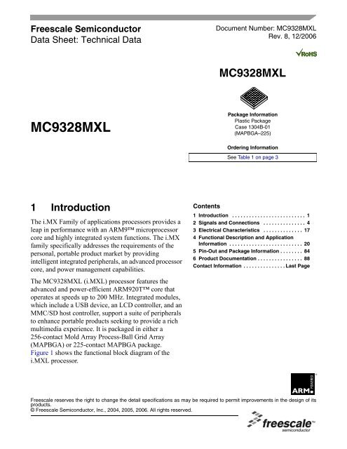
<strong>Freescale</strong> Semiconductor<br />
<strong>Data</strong> <strong>Sheet</strong>: Technical <strong>Data</strong><br />
<strong>MC9328MXL</strong><br />
1 Introduction<br />
The i.MX Family of applications processors provides a<br />
leap in performance with an ARM9 microprocessor<br />
core and highly integrated system functions. The i.MX<br />
family specifically addresses the requirements of the<br />
personal, portable product market by providing<br />
intelligent integrated peripherals, an advanced processor<br />
core, and power management capabilities.<br />
The <strong>MC9328MXL</strong> (i.MXL) processor features the<br />
advanced and power-efficient ARM920T core that<br />
operates at speeds up to 200 MHz. Integrated modules,<br />
which include a USB device, an LCD controller, and an<br />
MMC/SD host controller, support a suite of peripherals<br />
to enhance portable products seeking to provide a rich<br />
multimedia experience. It is packaged in either a<br />
256-contact Mold Array Process-Ball Grid Array<br />
(MAPBGA) or 225-contact MAPBGA package.<br />
Figure 1 shows the functional block diagram of the<br />
i.MXL processor.<br />
Document Number: <strong>MC9328MXL</strong><br />
Rev. 8, 12/2006<br />
<strong>MC9328MXL</strong><br />
Package Information<br />
Plastic Package<br />
Case 1304B-01<br />
(MAPBGA–225)<br />
Ordering Information<br />
See Table 1 on page 3<br />
Contents<br />
1 Introduction . . . . . . . . . . . . . . . . . . . . . . . . . . 1<br />
2 Signals and Connections . . . . . . . . . . . . . . . 4<br />
3 Electrical Characteristics . . . . . . . . . . . . . . 17<br />
4 Functional Description and Application<br />
Information . . . . . . . . . . . . . . . . . . . . . . . . . . 20<br />
5 Pin-Out and Package Information . . . . . . . . 84<br />
6 Product Documentation . . . . . . . . . . . . . . . . 88<br />
Contact Information . . . . . . . . . . . . . . . Last Page<br />
<strong>Freescale</strong> reserves the right to change the detail specifications as may be required to permit improvements in the design of its<br />
products.<br />
© <strong>Freescale</strong> Semiconductor, Inc., 2004, 2005, 2006. All rights reserved.
Introduction<br />
1.1 Features<br />
JTAG/ICE<br />
Connectivity<br />
MMC/SD<br />
Memory Stick®<br />
Host Controller<br />
SPI 1 and<br />
SPI 2<br />
UART 1<br />
UART 2<br />
SSI/I2S<br />
I2C<br />
USB Device<br />
System Control<br />
Bootstrap<br />
AIPI 1<br />
AIPI 2<br />
Power CGM<br />
Control (PLLx2)<br />
<strong>MC9328MXL</strong><br />
I Cache<br />
CPU Complex<br />
ARM9TDMI<br />
VMMU<br />
DMAC<br />
(11 Chnl)<br />
EIM &<br />
SDRAMC<br />
D Cache<br />
Interrupt<br />
Controller<br />
Bus<br />
Control<br />
Figure 1. i.MXL Functional Block Diagram<br />
To support a wide variety of applications, the processor offers a robust array of features, including the following:<br />
• ARM920T Microprocessor Core<br />
• AHB to IP Bus Interfaces (AIPIs)<br />
• External Interface Module (EIM)<br />
• SDRAM Controller (SDRAMC)<br />
• DPLL Clock and Power Control Module<br />
• Two Universal Asynchronous Receiver/Transmitters (UART 1 and UART 2)<br />
• Serial Peripheral Interface (SPI)<br />
• Two General-Purpose 32-bit Counters/Timers<br />
• Watchdog Timer<br />
• Real-Time Clock/Sampling Timer (RTC)<br />
• LCD Controller (LCDC)<br />
• Pulse-Width Modulation (PWM) Module<br />
• Universal Serial Bus (USB) Device<br />
• Multimedia Card and Secure Digital (MMC/SD) Host Controller Module<br />
• Memory Stick® Host Controller (MSHC)<br />
• Direct Memory Access Controller (DMAC)<br />
• Synchronous Serial Interface and an Inter-IC Sound (SSI/I 2 S) Module<br />
• Inter-IC (I 2 C) Bus Module<br />
<strong>MC9328MXL</strong> Technical <strong>Data</strong>, Rev. 8<br />
Standard<br />
System I/O<br />
Watchdog<br />
2 <strong>Freescale</strong> Semiconductor<br />
GPIO<br />
PWM<br />
Timer 1 & 2<br />
RTC<br />
Multimedia<br />
Multimedia<br />
Accelerator<br />
Video Port<br />
Human Interface<br />
LCD Controller
• Video Port<br />
• General-Purpose I/O (GPIO) Ports<br />
• Bootstrap Mode<br />
• Multimedia Accelerator (MMA)<br />
• Power Management Features<br />
• Operating Voltage Range: 1.7 V to 1.9 V core, 1.7 V to 3.3 V I/O<br />
• 256-pin MAPBGA Package<br />
• 225-contact MAPBGA Package<br />
1.2 Target <strong>Applications</strong><br />
<strong>MC9328MXL</strong> Technical <strong>Data</strong>, Rev. 8<br />
Introduction<br />
The i.MXL processor is targeted for advanced information appliances, smart phones, Web browsers,<br />
digital MP3 audio players, handheld computers, and messaging applications.<br />
1.3 Ordering Information<br />
Table 1 provides ordering information.<br />
1.4 Conventions<br />
This document uses the following conventions:<br />
Table 1. i.MXL Ordering Information<br />
Package Type Frequency Temperature Solderball Type Order Number<br />
256-lead MAPBGA 200 MHz 0 O C to 70 O C Pb-free <strong>MC9328MXL</strong>VM20(R2)<br />
-30 O C to 70 O C Pb-free <strong>MC9328MXL</strong>DVM20(R2)<br />
150 MHz 0 O C to 70 O C Pb-free <strong>MC9328MXL</strong>VM15(R2)<br />
-30 O C to 70 O C Pb-free <strong>MC9328MXL</strong>DVM15(R2)<br />
-40 O C to 85 O C Pb-free <strong>MC9328MXL</strong>CVM15(R2)<br />
225-lead MAPBGA 200 MHz 0 O C to 70 O C Pb-free <strong>MC9328MXL</strong>VP20(R2)<br />
-30 O C to 70 O C Pb-free <strong>MC9328MXL</strong>DVP20(R2)<br />
150 MHz 0°C to 70°C Pb-free <strong>MC9328MXL</strong>VP15(R2)<br />
-30 O C to 70 O C Pb-free <strong>MC9328MXL</strong>DVP15(R2)<br />
-40 O C to 85 O C Pb-free <strong>MC9328MXL</strong>CVP15(R2)<br />
• OVERBAR is used to indicate a signal that is active when pulled low: for example, RESET.<br />
• Logic level one is a voltage that corresponds to Boolean true (1) state.<br />
• Logic level zero is a voltage that corresponds to Boolean false (0) state.<br />
• To set a bit or bits means to establish logic level one.<br />
• To clear a bit or bits means to establish logic level zero.<br />
• A signal is an electronic construct whose state conveys or changes in state convey information.<br />
<strong>Freescale</strong> Semiconductor 3
Signals and Connections<br />
• A pin is an external physical connection. The same pin can be used to connect a number of signals.<br />
• Asserted means that a discrete signal is in active logic state.<br />
— Active low signals change from logic level one to logic level zero.<br />
— Active high signals change from logic level zero to logic level one.<br />
• Negated means that an asserted discrete signal changes logic state.<br />
— Active low signals change from logic level zero to logic level one.<br />
— Active high signals change from logic level one to logic level zero.<br />
• LSB means least significant bit or bits, and MSB means most significant bit or bits. References to<br />
low and high bytes or words are spelled out.<br />
• Numbers preceded by a percent sign (%) are binary. Numbers preceded by a dollar sign ($) or 0x<br />
are hexadecimal.<br />
2 Signals and Connections<br />
Table 2 identifies and describes the i.MXL processor signals that are assigned to package pins. The signals<br />
are grouped by the internal module that they are connected to.<br />
Table 2. i.MXL Signal Descriptions<br />
Signal Name Function/Notes<br />
External Bus/Chip-Select (EIM)<br />
A[24:0] Address bus signals<br />
D[31:0] <strong>Data</strong> bus signals<br />
EB0 MSB Byte Strobe—Active low external enable byte signal that controls D [31:24].<br />
EB1 Byte Strobe—Active low external enable byte signal that controls D [23:16].<br />
EB2 Byte Strobe—Active low external enable byte signal that controls D [15:8].<br />
EB3 LSB Byte Strobe—Active low external enable byte signal that controls D [7:0].<br />
OE Memory Output Enable—Active low output enables external data bus.<br />
CS [5:0] Chip-Select—The chip-select signals CS [3:2] are multiplexed with CSD [1:0] and are selected by the<br />
Function Multiplexing Control Register (FMCR). By default CSD [1:0] is selected.<br />
ECB Active low input signal sent by a flash device to the EIM whenever the flash device must terminate an<br />
on-going burst sequence and initiate a new (long first access) burst sequence.<br />
LBA Active low signal sent by a flash device causing the external burst device to latch the starting burst<br />
address.<br />
BCLK (burst clock) Clock signal sent to external synchronous memories (such as burst flash) during burst mode.<br />
RW RW signal—Indicates whether external access is a read (high) or write (low) cycle. Used as a WE input<br />
signal by external DRAM.<br />
DTACK DTACK signal—The external input data acknowledge signal. When using the external DTACK signal<br />
as a data acknowledge signal, the bus time-out monitor generates a bus error when a bus cycle is not<br />
terminated by the external DTACK signal after 1022 clock counts have elapsed.<br />
<strong>MC9328MXL</strong> Technical <strong>Data</strong>, Rev. 8<br />
4 <strong>Freescale</strong> Semiconductor
Bootstrap<br />
<strong>MC9328MXL</strong> Technical <strong>Data</strong>, Rev. 8<br />
Signals and Connections<br />
BOOT [3:0] System Boot Mode Select—The operational system boot mode of the i.MXL processor upon system<br />
reset is determined by the settings of these pins.<br />
SDRAM Controller<br />
SDBA [4:0] SDRAM non-interleave mode bank address multiplexed with address signals A [15:11]. These signals<br />
are logically equivalent to core address p_addr [25:21] in SDRAM cycles.<br />
SDIBA [3:0] SDRAM interleave addressing mode bank address multiplexed with address signals A [19:16]. These<br />
signals are logically equivalent to core address p_addr [12:9] in SDRAM cycles.<br />
MA [11:10] SDRAM address signals<br />
MA [9:0] SDRAM address signals which are multiplexed with address signals A [10:1]. MA [9:0] are selected on<br />
SDRAM cycles.<br />
DQM [3:0] SDRAM data enable<br />
CSD0 SDRAM Chip-select signal which is multiplexed with the CS2 signal. These two signals are selectable<br />
by programming the system control register.<br />
CSD1 SDRAM Chip-select signal which is multiplexed with CS3 signal. These two signals are selectable by<br />
programming the system control register. By default, CSD1 is selected, so it can be used as boot<br />
chip-select by properly configuring BOOT [3:0] input pins.<br />
RAS SDRAM Row Address Select signal<br />
CAS SDRAM Column Address Select signal<br />
SDWE SDRAM Write Enable signal<br />
SDCKE0 SDRAM Clock Enable 0<br />
SDCKE1 SDRAM Clock Enable 1<br />
SDCLK SDRAM Clock<br />
RESET_SF Not Used<br />
Clocks and Resets<br />
EXTAL16M Crystal input (4 MHz to 16 MHz), or a 16 MHz oscillator input when the internal oscillator circuit is shut<br />
down.<br />
XTAL16M Crystal output<br />
EXTAL32K 32 kHz crystal input<br />
XTAL32K 32 kHz crystal output<br />
Table 2. i.MXL Signal Descriptions (Continued)<br />
Signal Name Function/Notes<br />
CLKO Clock Out signal selected from internal clock signals.<br />
RESET_IN Master Reset—External active low Schmitt trigger input signal. When this signal goes active, all<br />
modules (except the reset module and the clock control module) are reset.<br />
RESET_OUT Reset Out—Internal active low output signal from the Watchdog Timer module and is asserted from the<br />
following sources: Power-on reset, External reset (RESET_IN), and Watchdog time-out.<br />
POR Power On Reset—Internal active high Schmitt trigger input signal. The POR signal is normally<br />
generated by an external RC circuit designed to detect a power-up event.<br />
<strong>Freescale</strong> Semiconductor 5
Signals and Connections<br />
TRST Test Reset Pin—External active low signal used to asynchronously initialize the JTAG controller.<br />
JTAG<br />
TDO Serial Output for test instructions and data. Changes on the falling edge of TCK.<br />
TDI Serial Input for test instructions and data. Sampled on the rising edge of TCK.<br />
TCK Test Clock to synchronize test logic and control register access through the JTAG port.<br />
TMS Test Mode Select to sequence the JTAG test controller’s state machine. Sampled on the rising edge of<br />
TCK.<br />
DMA<br />
DMA_REQ DMA Request—external DMA request signal. Multiplexed with SPI1_SPI_RDY.<br />
BIG_ENDIAN Big Endian—Input signal that determines the configuration of the external chip-select space. If it is<br />
driven logic-high at reset, the external chip-select space will be configured to big endian. If it is driven<br />
logic-low at reset, the external chip-select space will be configured to little endian. This input must not<br />
change state after power-on reset negates or during chip operation.<br />
ETMTRACESYNC ETM sync signal which is multiplexed with A24. ETMTRACESYNC is selected in ETM mode.<br />
ETMTRACECLK ETM clock signal which is multiplexed with A23. ETMTRACECLK is selected in ETM mode.<br />
ETM<br />
ETMPIPESTAT [2:0] ETM status signals which are multiplexed with A [22:20]. ETMPIPESTAT [2:0] are selected in ETM<br />
mode.<br />
ETMTRACEPKT [7:0] ETM packet signals which are multiplexed with ECB, LBA, BCLK (burst clock), PA17, A [19:16].<br />
ETMTRACEPKT [7:0] are selected in ETM mode.<br />
CSI_D [7:0] Sensor port data<br />
CSI_MCLK Sensor port master clock<br />
CSI_VSYNC Sensor port vertical sync<br />
CSI_HSYNC Sensor port horizontal sync<br />
CSI_PIXCLK Sensor port data latch clock<br />
CMOS Sensor Interface<br />
LCD Controller<br />
LD [15:0] LCD <strong>Data</strong> Bus—All LCD signals are driven low after reset and when LCD is off.<br />
FLM/VSYNC Frame Sync or Vsync—This signal also serves as the clock signal output for the gate<br />
driver (dedicated signal SPS for Sharp panel HR-TFT).<br />
LP/HSYNC Line pulse or H sync<br />
LSCLK Shift clock<br />
Table 2. i.MXL Signal Descriptions (Continued)<br />
Signal Name Function/Notes<br />
ACD/OE Alternate crystal direction/output enable.<br />
CONTRAST This signal is used to control the LCD bias voltage as contrast control.<br />
SPL_SPR Program horizontal scan direction (Sharp panel dedicated signal).<br />
PS Control signal output for source driver (Sharp panel dedicated signal).<br />
<strong>MC9328MXL</strong> Technical <strong>Data</strong>, Rev. 8<br />
6 <strong>Freescale</strong> Semiconductor
<strong>MC9328MXL</strong> Technical <strong>Data</strong>, Rev. 8<br />
Signals and Connections<br />
CLS Start signal output for gate driver. This signal is an inverted version of PS (Sharp panel dedicated<br />
signal).<br />
REV Signal for common electrode driving signal preparation (Sharp panel dedicated signal).<br />
SPI1_MOSI Master Out/Slave In<br />
SPI1_MISO Slave In/Master Out<br />
SPI1_SS Slave Select (Selectable polarity)<br />
SPI1_SCLK Serial Clock<br />
SPI1_SPI_RDY Serial <strong>Data</strong> Ready<br />
SPI 1 and SPI 2<br />
SPI2_TXD SPI2 Master Tx<strong>Data</strong> Output—This signal is multiplexed with a GPI/O pin yet shows up as a primary or<br />
alternative signal in the signal multiplex scheme table. Please refer to the SPI and GPIO chapters in<br />
the <strong>MC9328MXL</strong> Reference Manual for information about how to bring this signal to the assigned pin.<br />
SPI2_RXD SPI2 Master Rx<strong>Data</strong> Input—This signal is multiplexed with a GPI/O pin yet shows up as a primary or<br />
alternative signal in the signal multiplex scheme table. Please refer to the SPI and GPIO chapters in<br />
the <strong>MC9328MXL</strong> Reference Manual for information about how to bring this signal to the assigned pin.<br />
SPI2_SS SPI2 Slave Select—This signal is multiplexed with a GPI/O pin yet shows up as a primary or alternative<br />
signal in the signal multiplex scheme table. Please refer to the SPI and GPIO chapters in the<br />
<strong>MC9328MXL</strong> Reference Manual for information about how to bring this signal to the assigned pin.<br />
SPI2_SCLK SPI2 Serial Clock—This signal is multiplexed with a GPI/O pin yet shows up as a primary or alternative<br />
signal in the signal multiplex scheme table. Please refer to the SPI and GPIO chapters in the<br />
<strong>MC9328MXL</strong> Reference Manual for information about how to bring this signal to the assigned pin.<br />
General Purpose Timers<br />
TIN Timer Input Capture or Timer Input Clock—The signal on this input is applied to both timers<br />
simultaneously.<br />
TMR2OUT Timer 2 Output<br />
USBD_VMO USB Minus Output<br />
USBD_VPO USB Plus Output<br />
USBD_VM USB Minus Input<br />
USBD_VP USB Plus Input<br />
USBD_SUSPND USB Suspend Output<br />
USBD_RCV USB Receive <strong>Data</strong><br />
USBD_ROE USB OE<br />
USBD_AFE USB Analog Front End Enable<br />
USB Device<br />
Secure Digital Interface<br />
SD_CMD SD Command—If the system designer does not wish to make use of the internal pull-up, via the Pull-up<br />
enable register, a 4.7K–69K external pull up resistor must be added.<br />
SD_CLK MMC Output Clock<br />
Table 2. i.MXL Signal Descriptions (Continued)<br />
Signal Name Function/Notes<br />
<strong>Freescale</strong> Semiconductor 7
Signals and Connections<br />
SD_DAT [3:0] <strong>Data</strong>—If the system designer does not wish to make use of the internal pull-up, via the Pull-up enable<br />
register, a 50K–69K external pull up resistor must be added.<br />
Memory Stick Interface<br />
MS_BS Memory Stick Bus State (Output)—Serial bus control signal<br />
MS_SDIO Memory Stick Serial <strong>Data</strong> (Input/Output)<br />
MS_SCLKO Memory Stick Serial Clock (Input)—Serial protocol clock source for SCLK Divider<br />
MS_SCLKI Memory Stick External Clock (Output)—Test clock input pin for SCLK divider. This pin is only for test<br />
purposes, not for use in application mode.<br />
MS_PI0 General purpose Input0—Can be used for Memory Stick Insertion/Extraction detect<br />
MS_PI1 General purpose Input1—Can be used for Memory Stick Insertion/Extraction detect<br />
UART1_RXD Receive <strong>Data</strong><br />
UART1_TXD Transmit <strong>Data</strong><br />
UART1_RTS Request to Send<br />
UART1_CTS Clear to Send<br />
UART2_RXD Receive <strong>Data</strong><br />
UART2_TXD Transmit <strong>Data</strong><br />
UART2_RTS Request to Send<br />
UART2_CTS Clear to Send<br />
UART2_DSR <strong>Data</strong> Set Ready<br />
UART2_RI Ring Indicator<br />
UART2_DCD <strong>Data</strong> Carrier Detect<br />
UART2_DTR <strong>Data</strong> Terminal Ready<br />
SSI_TXDAT Transmit <strong>Data</strong><br />
SSI_RXDAT Receive <strong>Data</strong><br />
SSI_TXCLK Transmit Serial Clock<br />
SSI_RXCLK Receive Serial Clock<br />
SSI_TXFS Transmit Frame Sync<br />
SSI_RXFS Receive Frame Sync<br />
I2C_SCL I 2 C Clock<br />
I2C_SDA I 2 C <strong>Data</strong><br />
Table 2. i.MXL Signal Descriptions (Continued)<br />
Signal Name Function/Notes<br />
UARTs – IrDA/Auto-Bauding<br />
Serial Audio Port – SSI (configurable to I 2 S protocol)<br />
I 2 C<br />
<strong>MC9328MXL</strong> Technical <strong>Data</strong>, Rev. 8<br />
8 <strong>Freescale</strong> Semiconductor
PWMO PWM Output<br />
2.1 I/O Pads Power Supply and Signal Multiplexing Scheme<br />
PWM<br />
Test Function<br />
<strong>MC9328MXL</strong> Technical <strong>Data</strong>, Rev. 8<br />
Signals and Connections<br />
TRISTATE Forces all I/O signals to high impedance for test purposes. For normal operation, terminate this input<br />
with a 1 k ohm resistor to ground. (TRI-STATE ® is a registered trademark of National Semiconductor.)<br />
NVDD Digital Supply for the I/O pins<br />
NVSS Digital Ground for the I/O pins<br />
AVDD Supply for analog blocks<br />
Digital Supply Pins<br />
Supply Pins – Analog Modules<br />
Internal Power Supply<br />
QVDD Power supply pins for silicon internal circuitry<br />
QVSS Ground pins for silicon internal circuitry<br />
This section describes detailed information about both the power supply for each I/O pin and its function<br />
multiplexing scheme. The user can reference information provided in Table 6 on page 18 to configure the<br />
power supply scheme for each device in the system (memory and external peripherals). The function<br />
multiplexing information also shown in Table 6 allows the user to select the function of each pin by<br />
configuring the appropriate GPIO registers when those pins are multiplexed to provide different functions.<br />
I/O Supply<br />
Voltage<br />
225<br />
BGA<br />
Ball<br />
Table 3. <strong>MC9328MXL</strong>MC9328MXS Signal Multiplexing Scheme<br />
256<br />
BGA<br />
Ball<br />
Signal Dir<br />
Primary Alternate GPIO<br />
Pull-<br />
Up<br />
NVDD1 D2 B1 A24 O ETMTRAC<br />
ESYNC<br />
NVDD1 C1 C2 D31 I/O 69K<br />
NVDD1 D1 C1 A23 O ETMTRAC<br />
ECLK<br />
NVDD1 E3 D2 D30 I/O 69K<br />
NVDD1 E2 D1 A22 O ETMPIPE<br />
STAT2<br />
NVDD1 E4 D3 D29 I/O 69K<br />
NVDD1 E1 E2 A21 O ETMPIPE<br />
STAT1<br />
NVDD1 F3 E3 D28 I/O 69K<br />
Table 2. i.MXL Signal Descriptions (Continued)<br />
Signal Name Function/Notes<br />
Signal Dir Mux<br />
AIN BIN AOUT Default<br />
<strong>Freescale</strong> Semiconductor 9<br />
Pull<br />
-Up<br />
O PA0 69K SPI2_<br />
SCLK<br />
A24<br />
O PA31 69K A23<br />
O PA30 69K A22<br />
O PA29 69K A21
Signals and Connections<br />
I/O Supply<br />
Voltage<br />
Table 3. <strong>MC9328MXL</strong>MC9328MXS Signal Multiplexing Scheme (Continued)<br />
225<br />
BGA<br />
Ball<br />
256<br />
BGA<br />
Ball<br />
Signal Dir<br />
NVDD1 F1 E1 A20 O ETMPIPE<br />
STAT0<br />
NVDD1 F4 F2 D27 I/O 69K<br />
NVDD1 F2 F4 A19 O ETMTRAC<br />
EPKT3<br />
NVDD1 G3 E4 D26 I/O 69K<br />
NVDD1 G2 F1 A18 O ETMTRAC<br />
EPKT2<br />
NVDD1 G4 F3 D25 I/O 69K<br />
NVDD1 G1 G2 A17 O ETMTRAC<br />
EPKT1<br />
NVDD1 H4 G3 D24 I/O 69K<br />
NVDD1 H2 F5 A16 O ETMTRAC<br />
EPKT0<br />
NVDD1 H3 G4 D23 I/O 69K<br />
NVDD1 H1 G1 A15 O<br />
NVDD1 H5 H2 D22 I/O 69K<br />
NVDD1 J1 H3 A14 O<br />
NVDD1 J3 G5 D21 I/O 69K<br />
NVDD1 K1 H1 A13 O<br />
NVDD1 J4 H4 D20 I/O 69K<br />
NVDD1 J2 J1 A12 O<br />
NVDD1 K4 J4 D19 I/O 69K<br />
NVDD1 K2 J2 A11 O<br />
NVDD1 L4 J3 D18 I/O 69K<br />
NVDD1 L1 K1 A10 O<br />
NVDD1 L3 K4 D17 I/O 69K<br />
NVDD1 L2 K3 A9 O<br />
NVDD1 M1 K2 D16 I/O 69K<br />
NVDD1 N1 L1 A8 O<br />
NVDD1 M2 L4 D15 I/O 69K<br />
NVDD1 N2 L2 A7 O<br />
NVDD1 P1 L5 D14 I/O 69K<br />
NVDD1 R1 M4 A6 O<br />
NVDD1 M3 L3 D13 I/O 69K<br />
NVDD1 P2 M1 A5 O<br />
NVDD1 N3 M2 D12 I/O 69K<br />
NVDD1 P3 N1 A4 O<br />
NVDD1 R2 M3 D11 I/O 69K<br />
Primary Alternate GPIO<br />
Pull-<br />
Up<br />
Signal Dir Mux<br />
<strong>MC9328MXL</strong> Technical <strong>Data</strong>, Rev. 8<br />
AIN BIN AOUT Default<br />
O PA28 69K A20<br />
O PA27 69K A19<br />
O PA26 69K A18<br />
O PA25 69K A17<br />
O PA24 69K A16<br />
10 <strong>Freescale</strong> Semiconductor<br />
Pull<br />
-Up
I/O Supply<br />
Voltage<br />
Table 3. <strong>MC9328MXL</strong>MC9328MXS Signal Multiplexing Scheme (Continued)<br />
225<br />
BGA<br />
Ball<br />
256<br />
BGA<br />
Ball<br />
Signal Dir<br />
<strong>MC9328MXL</strong> Technical <strong>Data</strong>, Rev. 8<br />
Signals and Connections<br />
NVDD1 N4 P3 EB0 O<br />
NVDD1 M4 N3 D10 I/O 69K<br />
NVDD1 P4 P1 A3 O<br />
NVDD1 R3 N2 EB1 O<br />
NVDD1 N5 P2 D9 I/O 69K<br />
NVDD1 R4 R1 EB2 O<br />
NVDD1 P5 T2 A2 O<br />
NVDD1 M5 R2 EB3 O<br />
NVDD1 N6 R5 D8 I/O 69K<br />
NVDD1 R5 T3 OE O<br />
NVDD1 P6 R3 A1 O<br />
NVDD1 L7 T4 CS5 O PA23 69K PA23<br />
NVDD1 R6 N4 D7 I/O 69K<br />
NVDD1 M7 R4 CS4 O PA22 69K PA22<br />
NVDD1 R7 N5 A0 O PA21 69K A0<br />
NVDD1 N7 P4 CS3 O CSD1 CSD1<br />
NVDD1 P7 P5 D6 I/O 69K<br />
NVDD1 K3 T5 CS2 O CSD0 CSD0<br />
NVDD1 R8 M5 SDCLK O<br />
NVDD1 M8 T6 CS1 O<br />
NVDD1 N8 T7 CS0 O<br />
NVDD1 P8 R6 D5 I/O 69K<br />
NVDD1 L9 P6 ECB I ETMTRAC<br />
EPKT7<br />
PA20 69K ECB<br />
NVDD1 R9 N6 D4 I/O 69K<br />
NVDD1 R10 R7 LBA O ETMTRAC<br />
EPKT6<br />
NVDD1 R11 P8 D3 I/O 69K<br />
NVDD1 M9 R8 BCLK ETMTRAC<br />
EPKT5<br />
NVDD1 L8 P7 D2 I/O 69K<br />
NVDD1 N9 N7 PA17 ETMTRAC<br />
EPKT4<br />
NVDD1 K10 N8 D1 I/O 69K<br />
NVDD1 M10 M7 RW<br />
NVDD1 P10 T8 MA11 O<br />
NVDD1 P9 M8 MA10 O<br />
NVDD1 N10 R9 D0 I/O 69K<br />
NVDD1 R12 P9 DQM3 O<br />
Primary Alternate GPIO<br />
Pull-<br />
Up<br />
Signal Dir Mux<br />
PA19 69K LBA<br />
PA18 69K BCLK<br />
PA17 69K SPI2_<br />
SS<br />
AIN BIN AOUT Default<br />
DTACK PA17<br />
<strong>Freescale</strong> Semiconductor 11<br />
Pull<br />
-Up
Signals and Connections<br />
I/O Supply<br />
Voltage<br />
Table 3. <strong>MC9328MXL</strong>MC9328MXS Signal Multiplexing Scheme (Continued)<br />
225<br />
BGA<br />
Ball<br />
256<br />
BGA<br />
Ball<br />
Signal Dir<br />
NVDD1 N11 T9 DQM2 O<br />
NVDD1 P11 N9 DQM1 O<br />
NVDD1 N12 R10 DQM0 O<br />
NVDD1 P12 M9 RAS O<br />
NVDD1 R13 L8 CAS O<br />
NVDD1 R14 T10 SDWE O<br />
NVDD1 N13 R11 SDCKE0 O<br />
NVDD1 P13 P10 SDCKE1 O<br />
NVDD1 P15 N10 RESET_S<br />
F<br />
O<br />
NVDD1 P14 T11 CLKO O<br />
AVDD1 R15 T12 AVDD1 Static<br />
QVDD2 M13 R15 QVDD2 Static<br />
AVDD1 N15 P13 TRST I 69K<br />
AVDD1 N14 T13 TRISTATE<br />
1<br />
I<br />
AVDD1 M15 T14 EXTAL16<br />
M<br />
AVDD1 L14 T15 XTAL16M O<br />
AVDD1 L15 R16 EXTAL32<br />
K<br />
I<br />
AVDD1 K15 P16 XTAL32K O<br />
AVDD1 M14 M10 RESET_I<br />
N 2<br />
I 69K<br />
AVDD1 K14 N11 RESET_O<br />
UT<br />
AVDD1 L12 R12 POR 2 I<br />
AVDD1 K13 M11 BIG_ENDI<br />
AN 3<br />
AVDD1 M12 P11 BOOT3 3 I<br />
AVDD1 K11 N12 BOOT2 3 I<br />
AVDD1 J14 R13 BOOT1 3 I<br />
AVDD1 J15 P12 BOOT0 3 I<br />
NVDD2 J13 R14 TDO 4 O<br />
Primary Alternate GPIO<br />
I<br />
O<br />
I<br />
Pull-<br />
Up<br />
Signal Dir Mux<br />
NVDD2 H15 N15 TMS I 69K<br />
NVDD2 J12 L9 TCK I 69K<br />
NVDD2 K12 N16 TDI I 69K<br />
NVDD2 J11 P14 I2C_SCL O PA16 69K PA16<br />
NVDD2 H14 P15 I2C_SDA I/O PA15 69K PA15<br />
<strong>MC9328MXL</strong> Technical <strong>Data</strong>, Rev. 8<br />
AIN BIN AOUT Default<br />
12 <strong>Freescale</strong> Semiconductor<br />
Pull<br />
-Up
I/O Supply<br />
Voltage<br />
Table 3. <strong>MC9328MXL</strong>MC9328MXS Signal Multiplexing Scheme (Continued)<br />
225<br />
BGA<br />
Ball<br />
256<br />
BGA<br />
Ball<br />
Signal Dir<br />
NVDD2 H13 N13 CSI_PIXC<br />
LK<br />
NVDD2 G14 M13 CSI_HSY<br />
NC<br />
NVDD2 H12 M14 CSI_VSY<br />
NC<br />
Primary Alternate GPIO<br />
Pull-<br />
Up<br />
Signal Dir Mux<br />
<strong>MC9328MXL</strong> Technical <strong>Data</strong>, Rev. 8<br />
Signals and Connections<br />
I PA14 69K PA14<br />
I PA13 69K PA13<br />
I PA12 69K PA12<br />
NVDD2 G13 N14 CSI_D7 I PA11 69K PA11<br />
NVDD2 J10 M15 CSI_D6 I PA10 69K PA10<br />
NVDD2 G15 M16 CSI_D5 I PA9 69K PA9<br />
NVDD2 F15 M12 CSI_D4 I PA8 69K PA8<br />
NVDD2 G12 L16 CSI_D3 I PA7 69K PA7<br />
NVDD2 F14 L15 CSI_D2 I PA6 69K PA6<br />
NVDD2 H11 L14 CSI_D1 I PA5 69K PA5<br />
NVDD2 E14 L13 CSI_D0 I PA4 69K PA4<br />
NVDD2 E15 L12 CSI_MCL<br />
K<br />
O PA3 69K PA3<br />
NVDD2 G11 L11 PWMO O PA2 69K PA2<br />
NVDD2 E13 L10 TIN I PA1 69K SPI2_<br />
RXD_0<br />
PA1<br />
NVDD2 D14 K15 TMR2OUT O PD31 69K SPI2_<br />
TXD<br />
AIN BIN AOUT Default<br />
NVDD2 F13 K16 LD15 O PD30 69K PD30<br />
NVDD2 F12 K14 LD14 O PD29 69K PD29<br />
NVDD2 D15 K13 LD13 O PD28 69K PD28<br />
NVDD2 C14 K12 LD12 O PD27 69K PD27<br />
NVDD2 D13 J14 LD11 O PD26 69K PD26<br />
NVDD2 E12 K11 LD10 O PD25 69K PD25<br />
NVDD2 C13 H15 LD9 O PD24 69K PD24<br />
NVDD2 C12 J13 LD8 O PD23 69K PD23<br />
NVDD2 B15 J12 LD7 O PD22 69K PD22<br />
NVDD2 B14 J11 LD6 O PD21 69K PD21<br />
NVDD2 A15 H14 LD5 O PD20 69K PD20<br />
NVDD2 A14 H13 LD4 O PD19 69K PD19<br />
NVDD2 B13 H16 LD3 O PD18 69K PD18<br />
NVDD2 A13 H12 LD2 O PD17 69K PD17<br />
NVDD2 D12 G16 LD1 O PD16 69K PD16<br />
NVDD2 B12 H11 LD0 O PD15 69K PD15<br />
NVDD2 C11 G15 FLM/VSY<br />
NC<br />
O PD14 69K PD14<br />
<strong>Freescale</strong> Semiconductor 13<br />
Pull<br />
-Up<br />
PD31
Signals and Connections<br />
I/O Supply<br />
Voltage<br />
Table 3. <strong>MC9328MXL</strong>MC9328MXS Signal Multiplexing Scheme (Continued)<br />
225<br />
BGA<br />
Ball<br />
256<br />
BGA<br />
Ball<br />
Signal Dir<br />
NVDD2 D11 G14 LP/HSYN<br />
C<br />
O PD13 69K PD13<br />
NVDD2 E11 G13 ACD/OE O PD12 69K PD12<br />
NVDD2 C10 G12 CONTRA<br />
ST<br />
O PD11 69K PD11<br />
NVDD2 B11 F16 SPL_SPR O UART2_D<br />
SR<br />
<strong>MC9328MXL</strong> Technical <strong>Data</strong>, Rev. 8<br />
O PD10 69K SPI2_<br />
TXD<br />
NVDD2 A12 H10 PS O UART2_RI O PD9 69K SPI2_<br />
RXD_1<br />
NVDD2 F10 G11 CLS O UART2_D<br />
CD<br />
NVDD2 A11 F12 REV O UART2_D<br />
TR<br />
O PD8 69K SPI2_<br />
SS<br />
I PD7 69K SPI2_<br />
SCLK<br />
NVDD2 B10 F15 LSCLK O PD6 69K PD6<br />
NVDD3 D10 G9 SPI1_MO<br />
SI<br />
I/O PC17 69K PC17<br />
NVDD3 E10 F9 SPI1_MIS<br />
O<br />
14 <strong>Freescale</strong> Semiconductor<br />
PD10<br />
PD9<br />
PD8<br />
PD7<br />
I/O PC16 69K PC16<br />
NVDD3 B9 E9 SPI1_SS I/O PC15 69K PC15<br />
NVDD3 A10 B9 SPI1_SCL<br />
K<br />
I/O PC14 69K PC14<br />
NVDD3 A9 D9 SPI1_SPI<br />
_RDY<br />
NVDD3 E8 A9 UART1_R<br />
XD<br />
NVDD3 B8 C9 UART1_T<br />
XD<br />
NVDD3 C9 A8 UART1_R<br />
TS<br />
NVDD3 E9 G8 UART1_C<br />
TS<br />
NVDD3 A8 B8 SSI_TXCL<br />
K<br />
I/O PC13 69K DMA_REQ PC13<br />
I PC12 69K PC12<br />
O PC11 69K PC11<br />
I PC10 69K PC10<br />
O PC9 69K PC9<br />
I/O PC8 69K PC8<br />
NVDD3 C8 F8 SSI_TXFS I/O PC7 69K PC7<br />
NVDD3 F9 E8 SSI_TXDA<br />
T<br />
O PC6 69K PC6<br />
NVDD3 B7 D8 SSI_RXD<br />
AT<br />
NVDD3 F8 B7 SSI_RXCL<br />
K<br />
Primary Alternate GPIO<br />
Pull-<br />
Up<br />
Signal Dir Mux<br />
AIN BIN AOUT Default<br />
I PC5 69K PC5<br />
I PC4 69K PC4<br />
NVDD3 A7 C8 SSI_RXFS I PC3 69K PC3<br />
NVDD4 C7 C7 UART2_R<br />
XD<br />
I PB31 69K PB31<br />
Pull<br />
-Up
I/O Supply<br />
Voltage<br />
Table 3. <strong>MC9328MXL</strong>MC9328MXS Signal Multiplexing Scheme (Continued)<br />
225<br />
BGA<br />
Ball<br />
256<br />
BGA<br />
Ball<br />
Signal Dir<br />
NVDD4 D8 F7 UART2_T<br />
XD<br />
NVDD4 E7 E7 UART2_R<br />
TS<br />
NVDD4 F7 C6 UART2_C<br />
TS<br />
NVDD4 B6 D7 USBD_VM<br />
O<br />
NVDD4 C6 D6 USBD_VP<br />
O<br />
<strong>MC9328MXL</strong> Technical <strong>Data</strong>, Rev. 8<br />
Signals and Connections<br />
O PB30 69K PB30<br />
I PB29 69K PB29<br />
O PB28 69K PB28<br />
O PB27 69K PB27<br />
O PB26 69K PB26<br />
NVDD4 A6 E6 USBD_VM I PB25 69K PB25<br />
NVDD4 D6 B6 USBD_VP I PB24 69K PB24<br />
NVDD4 A5 D5 USBD_SU<br />
SPND<br />
NVDD4 B5 C5 USBD_RC<br />
V<br />
NVDD4 A4 B5 USBD_RO<br />
E<br />
NVDD4 B4 A5 USBD_AF<br />
E<br />
Primary Alternate GPIO<br />
Pull-<br />
Up<br />
O PB23 69K PB23<br />
I/O PB22 69K PB22<br />
O PB21 69K PB21<br />
O PB20 69K PB20<br />
NVDD4 A3 G7 PB19 I/O 69K PB19<br />
NVDD4 C4 F6 PB18 I/O 69K PB18<br />
NVDD4 D4 G6 PB17 O 69K PB17<br />
NVDD4 B3 B4 PB16 I 69K PB16<br />
NVDD4 A2 C4 PB15 I 69K PB15<br />
NVDD4 C3 D4 PB14 I 69K PB14<br />
NVDD4 A1 B3 SD_CMD I/O MS_BS PB13 69K PB13<br />
NVDD4 B2 A3 SD_CLK O MS_SCLK<br />
O<br />
PB12 69K PB12<br />
NVDD4 B1 A2 SD_DAT3 I/O MS_SDIO PB11 69K<br />
(pull<br />
down)<br />
NVDD4 C5 E5 SD_DAT2 I/O MS_SCLK<br />
I<br />
Signal Dir Mux<br />
AIN BIN AOUT Default<br />
<strong>Freescale</strong> Semiconductor 15<br />
PB11<br />
PB10 69K PB10<br />
NVDD4 D3 B2 SD_DAT1 I/O MS_PI1 PB9 69K PB9<br />
NVDD4 C2 C3 SD_DAT0 I/O MS_PI0 PB8 69K PB8<br />
NVDD1 D5 K8 NVDD1 Static<br />
G6 A1 NVSS Static<br />
NVDD1 E5 H5 NVDD1 Static<br />
H6 T1 NVSS Static<br />
QVDD1 J8 H9 QVDD1 Static<br />
E6 H8 QVSS Static<br />
Pull<br />
-Up
Signals and Connections<br />
I/O Supply<br />
Voltage<br />
Table 3. <strong>MC9328MXL</strong>MC9328MXS Signal Multiplexing Scheme (Continued)<br />
225<br />
BGA<br />
Ball<br />
256<br />
BGA<br />
Ball<br />
Signal Dir<br />
NVDD1 F5 J5 NVDD Static<br />
J6 K6 NVSS Static<br />
NVDD1 G5 K5 NVDD1 Static<br />
K6 M6 NVSS Static<br />
NVDD1 J5 H6 NVDD1 Static<br />
H7 J7 NVSS Static<br />
NVDD1 K5 L6 NVDD1 Static<br />
J7 J7 NVSS Static<br />
NVDD1 L5 L6 NVDD1 Static<br />
G8 K7 NVSS Static<br />
NVDD1 L5 J8 NVDD1 Static<br />
H8 L7 NVSS Static<br />
K7 T16 QVSS Static<br />
NVDD2 H10 K10 NVDD2 Static<br />
G9 J10 NVSS Static<br />
QVDD3 F11 J15 QVDD3 Static<br />
G10 J16 QVSS Static<br />
NVDD2 C15 K9 NVDD2 Static<br />
H9 J9 NVSS Static<br />
QVDD4 D7 A13 QVDD4 Static<br />
L13 B13 QVSS Static<br />
NVDD3 D9 A10 NVDD3 Static<br />
J9 A7 NVSS Static<br />
K9 A4 NVSS Static<br />
NVDD4 G7 A6 NVDD4 Static<br />
NVDD1 F6 NVDD1 Static<br />
NVDD1 L6 NVDD1 Static<br />
NVDD1 M6 NVDD1 Static<br />
NVDD1 K8 NVDD1 Static<br />
L10 NVSS Static<br />
L11 NVSS Static<br />
M11 NVSS Static<br />
1 Pull down this input with 1KΩ resistor to GND.<br />
2<br />
External circuit required to drive this input.<br />
3 Tie this input high (to AVDD) or pull down with 1KΩ resistor to GND.<br />
4 Pull up this output with a resistor to NVDD2.<br />
Primary Alternate GPIO<br />
Pull-<br />
Up<br />
Signal Dir Mux<br />
<strong>MC9328MXL</strong> Technical <strong>Data</strong>, Rev. 8<br />
AIN BIN AOUT Default<br />
16 <strong>Freescale</strong> Semiconductor<br />
Pull<br />
-Up
3 Electrical Characteristics<br />
<strong>MC9328MXL</strong> Technical <strong>Data</strong>, Rev. 8<br />
Electrical Characteristics<br />
This section contains the electrical specifications and timing diagrams for the i.MXL processor.<br />
3.1 Maximum Ratings<br />
Table 4 provides information on maximum ratings which are those values beyond which damage to the<br />
device may occur. Functional operation should be restricted to the limits listed in Recommended Operating<br />
Range Table 5 on page 18 or the DC Characteristics table.<br />
Table 4. Maximum Ratings<br />
Symbol Rating Minimum Maximum Unit<br />
NV DD DC I/O Supply Voltage -0.3 3.3 V<br />
QV DD DC Internal (core = 150 MHz) Supply Voltage -0.3 1.9 V<br />
QV DD DC Internal (core = 200 MHz) Supply Voltage -0.3 2.0 V<br />
AV DD DC Analog Supply Voltage -0.3 3.3 V<br />
BTRFV DD DC Bluetooth Supply Voltage -0.3 3.3 V<br />
VESD_HBM ESD immunity with HBM (human body model) – 2000 V<br />
VESD_MM ESD immunity with MM (machine model) – 100 V<br />
ILatchup Latch-up immunity – 200 mA<br />
Test Storage temperature -55 150 °C<br />
Pmax Power Consumption 800 1<br />
1300<br />
1 ®<br />
A typical application with 30 pads simultaneously switching assumes the GPIO toggling and instruction fetches from the ARM<br />
core-that is, 7x GPIO, 15x <strong>Data</strong> bus, and 8x Address bus.<br />
2 mW<br />
2<br />
A worst-case application with 70 pads simultaneously switching assumes the GPIO toggling and instruction fetches from the<br />
ARM core-that is, 32x GPIO, 30x <strong>Data</strong> bus, 8x Address bus. These calculations are based on the core running its heaviest OS<br />
application at 200MHz, and where the whole image is running out of SDRAM. QVDD at 2.0V, NVDD and AVDD at 3.3V,<br />
therefore, 180mA is the worst measurement recorded in the factory environment, max 5mA is consumed for OSC pads, with<br />
each toggle GPIO consuming 4mA.<br />
3.2 Recommended Operating Range<br />
Table 5 provides the recommended operating ranges for the supply voltages and temperatures. The i.MXL<br />
processor has multiple pairs of VDD and VSS power supply and return pins. QVDD and QVSS pins are<br />
used for internal logic. All other VDD and VSS pins are for the I/O pads voltage supply, and each pair of<br />
VDD and VSS provides power to the enclosed I/O pads. This design allows different peripheral supply<br />
voltage levels in a system.<br />
Because AVDD pins are supply voltages to the analog pads, it is recommended to isolate and noise-filter<br />
the AVDD pins from other VDD pins.<br />
For more information about I/O pads grouping per VDD, please refer to Table 2 on page 4.<br />
<strong>Freescale</strong> Semiconductor 17
Electrical Characteristics<br />
3.3 Power Sequence Requirements<br />
For required power-up and power-down sequencing, please refer to the “Power-Up Sequence” section of<br />
application note AN2537 on the i.MX applications processor website.<br />
3.4 DC Electrical Characteristics<br />
Table 5. Recommended Operating Range<br />
Symbol Rating Minimum Maximum Unit<br />
T A<br />
T A<br />
T A<br />
Operating temperature range<br />
<strong>MC9328MXL</strong>VM20/<strong>MC9328MXL</strong>VM15<br />
<strong>MC9328MXL</strong>VP20/<strong>MC9328MXL</strong>VP15<br />
Operating temperature range<br />
<strong>MC9328MXL</strong>DVM20/<strong>MC9328MXL</strong>DVM15<br />
<strong>MC9328MXL</strong>DVP20/<strong>MC9328MXL</strong>DVP15<br />
Operating temperature range<br />
<strong>MC9328MXL</strong>CVM15/<br />
<strong>MC9328MXL</strong>CVP15<br />
NVDD I/O supply voltage (if using MSHC, CSI, SPI, LCD, and USBd which are<br />
only 3 V interfaces)<br />
Table 6 contains both maximum and minimum DC characteristics of the i.MXL processor.<br />
<strong>MC9328MXL</strong> Technical <strong>Data</strong>, Rev. 8<br />
0 70 °C<br />
-30 70 °C<br />
-40 85 °C<br />
2.70 3.30 V<br />
NVDD I/O supply voltage (if not using the peripherals listed above) 1.70 3.30 V<br />
QVDD Internal supply voltage (Core = 150 MHz) 1.70 1.90 V<br />
QVDD Internal supply voltage (Core = 200 MHz) 1.80 2.00 V<br />
AVDD Analog supply voltage 1.70 3.30 V<br />
Number or<br />
Symbol<br />
Table 6. Maximum and Minimum DC Characteristics<br />
Iop Full running operating current at 1.8V for QVDD, 3.3V for<br />
NVDD/AVDD (Core = 96 MHz, System = 96 MHz, MPEG4<br />
decoding playback from external memory card to both<br />
external SSI audio decoder and driving TFT display panel,<br />
and OS with MMU enabled memory system is running on<br />
external SDRAM).<br />
Sidd 1<br />
Sidd 2<br />
Sidd 3<br />
Sidd 4<br />
Standby current<br />
(Core = 150 MHz, QVDD = 1.8V, temp = 25°C)<br />
Standby current<br />
(Core = 150 MHz, QVDD = 1.8V, temp = 55°C)<br />
Standby current<br />
(Core = 150 MHz, QVDD = 2.0V, temp = 25°C)<br />
Standby current<br />
(Core = 150 MHz, QVDD = 2.0V, temp = 55°C)<br />
Parameter Min Typical Max Unit<br />
– QVDD at<br />
1.8V = 120mA;<br />
NVDD+AVDD at<br />
3.0V = 30mA<br />
– mA<br />
– 25 – μA<br />
– 45 – μA<br />
– 35 – μA<br />
– 60 – μA<br />
18 <strong>Freescale</strong> Semiconductor
Number or<br />
Symbol<br />
3.5 AC Electrical Characteristics<br />
<strong>MC9328MXL</strong> Technical <strong>Data</strong>, Rev. 8<br />
Electrical Characteristics<br />
V IH Input high voltage 0.7V DD – Vdd+0.2 V<br />
V IL Input low voltage – – 0.4 V<br />
V OH Output high voltage (I OH = 2.0 mA) 0.7V DD – Vdd V<br />
V OL Output low voltage (I OL = -2.5 mA) – – 0.4 V<br />
I IL<br />
I IH<br />
I OH<br />
I OL<br />
I OZ<br />
Table 6. Maximum and Minimum DC Characteristics (Continued)<br />
Input low leakage current<br />
(V IN = GND, no pull-up or pull-down)<br />
Input high leakage current<br />
(V IN =V DD , no pull-up or pull-down)<br />
Output high current<br />
(V OH =0.8V DD , V DD =1.8V)<br />
Output low current<br />
(V OL =0.4V, V DD =1.8V)<br />
Output leakage current<br />
(V out =V DD , output is high impedance)<br />
Parameter Min Typical Max Unit<br />
– – ±1 μA<br />
– – ±1 μA<br />
4.0 – – mA<br />
-4.0 – – mA<br />
– – ±5 μA<br />
C i Input capacitance – – 5 pF<br />
C o Output capacitance – – 5 pF<br />
The AC characteristics consist of output delays, input setup and hold times, and signal skew times. All<br />
signals are specified relative to an appropriate edge of other signals. All timing specifications are specified<br />
at a system operating frequency from 0 MHz to 96 MHz (core operating frequency 150 MHz) with an<br />
operating supply voltage from V DD min to V DD max under an operating temperature from T L to T H . All<br />
timing is measured at 30 pF loading.<br />
Table 7. Tristate Signal Timing<br />
Pin Parameter Minimum Maximum Unit<br />
TRISTATE Time from TRISTATE activate until I/O becomes Hi-Z – 20.8 ns<br />
Table 8. 32k/16M Oscillator Signal Timing<br />
Parameter Minimum RMS Maximum Unit<br />
EXTAL32k input jitter (peak to peak) – 5 20 ns<br />
EXTAL32k startup time 800 – – ms<br />
EXTAL16M input jitter (peak to peak) 1<br />
– TBD TBD –<br />
EXTAL16M startup time 1 TBD – – –<br />
1 The 16 MHz oscillator is not recommended for use in new designs.<br />
<strong>Freescale</strong> Semiconductor 19
Functional Description and Application Information<br />
4 Functional Description and Application Information<br />
This section provides the electrical information including and timing diagrams for the individual modules<br />
of the i.MXL.<br />
4.1 Embedded Trace Macrocell<br />
All registers in the ETM9 are programmed through a JTAG interface. The interface is an extension of the<br />
ARM920T processor’s TAP controller, and is assigned scan chain 6. The scan chain consists of a 40-bit<br />
shift register comprised of the following:<br />
• 32-bit data field<br />
• 7-bit address field<br />
• A read/write bit<br />
The data to be written is scanned into the 32-bit data field, the address of the register into the 7-bit address<br />
field, and a 1 into the read/write bit.<br />
A register is read by scanning its address into the address field and a 0 into the read/write bit. The 32-bit<br />
data field is ignored. A read or a write takes place when the TAP controller enters the UPDATE-DR state.<br />
The timing diagram for the ETM9 is shown in Figure 2. See Table 9 for the ETM9 timing parameters used<br />
in Figure 2.<br />
TRACECLK<br />
TRACECLK<br />
(Half-Rate Clocking Mode)<br />
Output Trace Port<br />
Ref No. Parameter<br />
3a<br />
2a<br />
3b<br />
Figure 2. Trace Port Timing Diagram<br />
Table 9. Trace Port Timing Diagram Parameter Table<br />
1.8 ± 0.1 V 3.0 ± 0.3 V<br />
Minimum Maximum Minimum Maximum<br />
1 CLK frequency 0 85 0 100 MHz<br />
2a Clock high time 1.3 – 2 – ns<br />
2b Clock low time 3 – 2 – ns<br />
3a Clock rise time – 4 – 3 ns<br />
3b Clock fall time – 3 – 3 ns<br />
<strong>MC9328MXL</strong> Technical <strong>Data</strong>, Rev. 8<br />
20 <strong>Freescale</strong> Semiconductor<br />
2b<br />
4a<br />
1<br />
Valid <strong>Data</strong> Valid <strong>Data</strong><br />
4b<br />
Unit
Ref No. Parameter<br />
4.2 DPLL Timing Specifications<br />
<strong>MC9328MXL</strong> Technical <strong>Data</strong>, Rev. 8<br />
Functional Description and Application Information<br />
4a Output hold time 2.28 – 2 – ns<br />
4b Output setup time 3.42 – 3 – ns<br />
Parameters of the DPLL are given in Table 10. In this table, T ref is a reference clock period after the<br />
pre-divider and T dck is the output double clock period.<br />
Table 10. DPLL Specifications<br />
Parameter Test Conditions Minimum Typical Maximum Unit<br />
DPLL input clock freq range Vcc = 1.8V 5 – 100 MHz<br />
Pre-divider output clock<br />
freq range<br />
Vcc = 1.8V<br />
5 – 30 MHz<br />
DPLL output clock freq range Vcc = 1.8V 80 – 220 MHz<br />
Pre-divider factor (PD) – 1 – 16 –<br />
Total multiplication factor (MF) Includes both integer and fractional parts 5 – 15 –<br />
MF integer part – 5 – 15 –<br />
MF numerator Should be less than the denominator 0 – 1022 –<br />
MF denominator – 1 – 1023 –<br />
Pre-multiplier lock-in time – – – 312.5 μsec<br />
Freq lock-in time after<br />
full reset<br />
Freq lock-in time after<br />
partial reset<br />
Phase lock-in time after<br />
full reset<br />
Phase lock-in time after<br />
partial reset<br />
Freq jitter (p-p) –<br />
Table 9. Trace Port Timing Diagram Parameter Table (Continued)<br />
FOL mode for non-integer MF<br />
(does not include pre-multi lock-in time)<br />
FOL mode for non-integer MF (does not<br />
include pre-multi lock-in time)<br />
FPL mode and integer MF (does not include<br />
pre-multi lock-in time)<br />
FPL mode and integer MF (does not include<br />
pre-multi lock-in time)<br />
<strong>Freescale</strong> Semiconductor 21<br />
250<br />
220<br />
300<br />
270<br />
–<br />
280<br />
(56 μs)<br />
250<br />
(50 μs)<br />
350<br />
(70 μs)<br />
320<br />
(64 μs)<br />
0.005<br />
(0.01%)<br />
300 T ref<br />
270 T ref<br />
400 T ref<br />
370 T ref<br />
0.01 2 T dck<br />
Phase jitter (p-p) Integer MF, FPL mode, Vcc=1.8V<br />
–<br />
1.0<br />
(10%)<br />
1.5 ns<br />
Power supply voltage – 1.7 – 2.5 V<br />
Power dissipation FOL mode, integer MF,<br />
f dck = 200 MHz, Vcc = 1.8V<br />
1.8 ± 0.1 V 3.0 ± 0.3 V<br />
Minimum Maximum Minimum Maximum<br />
Unit<br />
– – 4 mW
Functional Description and Application Information<br />
4.3 Reset Module<br />
The timing relationships of the Reset module with the POR and RESET_IN are shown in Figure 3 and<br />
Figure 4.<br />
NOTE<br />
Be aware that NVDD must ramp up to at least 1.8V before QVDD is powered up<br />
to prevent forward biasing.<br />
POR<br />
RESET_POR<br />
RESET_DRAM<br />
HRESET<br />
RESET_OUT<br />
CLK32<br />
HCLK<br />
RESET_IN<br />
HRESET<br />
RESET_OUT<br />
CLK32<br />
HCLK<br />
90% AVDD<br />
6<br />
1<br />
10% AVDD<br />
Figure 3. Timing Relationship with POR<br />
5<br />
Figure 4. Timing Relationship with RESET_IN<br />
<strong>MC9328MXL</strong> Technical <strong>Data</strong>, Rev. 8<br />
22 <strong>Freescale</strong> Semiconductor<br />
2<br />
Exact 300ms<br />
3<br />
4<br />
7 cycles @ CLK32<br />
14 cycles @ CLK32<br />
14 cycles @ CLK32<br />
4
Ref<br />
No.<br />
4.4 External Interface Module<br />
Table 11. Reset Module Timing Parameter Table<br />
Parameter<br />
1 Width of input POWER_ON_RESET note 1<br />
2 Width of internal POWER_ON_RESET<br />
(CLK32 at 32 kHz)<br />
<strong>MC9328MXL</strong> Technical <strong>Data</strong>, Rev. 8<br />
Functional Description and Application Information<br />
1.8 ± 0.1 V 3.0 ± 0.3 V<br />
Min Max Min Max<br />
1 POR width is dependent on the 32 or 32.768 kHz crystal oscillator start-up time. Design margin should allow for crystal<br />
tolerance, i.MX chip variations, temperature impact, and supply voltage influence. Through the process of supplying crystals<br />
for use with CMOS oscillators, crystal manufacturers have developed a working knowledge of start-up time of their crystals.<br />
Typically, start-up times range from 400 ms to 1.2 seconds for this type of crystal.<br />
If an external stable clock source (already running) is used instead of a crystal, the width of POR should be ignored in<br />
calculating timing for the start-up process.<br />
The External Interface Module (EIM) handles the interface to devices external to the i.MXL processor,<br />
including the generation of chip-selects for external peripherals and memory. The timing diagram for the<br />
EIM is shown in Figure 5, and Table 12 defines the parameters of signals.<br />
<strong>Freescale</strong> Semiconductor 23<br />
Unit<br />
– note 1 – –<br />
300 300 300 300 ms<br />
3 7K to 32K-cycle stretcher for SDRAM reset 7 7 7 7 Cycles of<br />
CLK32<br />
4 14K to 32K-cycle stretcher for internal system reset<br />
HRESERT and output reset at pin RESET_OUT<br />
14 14 14 14 Cycles of<br />
CLK32<br />
5 Width of external hard-reset RESET_IN 4 – 4 – Cycles of<br />
CLK32<br />
6 4K to 32K-cycle qualifier 4 4 4 4 Cycles of<br />
CLK32
Functional Description and Application Information<br />
(HCLK) Bus Clock<br />
Address<br />
Chip-select<br />
Read (Write)<br />
OE (rising edge)<br />
OE (falling edge)<br />
EB (rising edge)<br />
EB (falling edge)<br />
LBA (negated falling edge)<br />
LBA (negated rising edge)<br />
BCLK (burst clock) - rising edge<br />
BCLK (burst clock) - falling edge<br />
Read <strong>Data</strong><br />
Write <strong>Data</strong> (negated falling)<br />
Write <strong>Data</strong> (negated rising)<br />
DTACK_B<br />
Ref No. Parameter<br />
1a 1b<br />
2a 2b<br />
3a<br />
6a<br />
6a<br />
4a 4b<br />
4c 4d<br />
5a 5b<br />
5c 5d<br />
Figure 5. EIM Bus Timing Diagram<br />
Table 12. EIM Bus Timing Parameter Table<br />
<strong>MC9328MXL</strong> Technical <strong>Data</strong>, Rev. 8<br />
1.8 ± 0.1 V 3.0 ± 0.3 V<br />
Min Typical Max Min Typical Max<br />
1a Clock fall to address valid 2.48 3.31 9.11 2.4 3.2 8.8 ns<br />
1b Clock fall to address invalid 1.55 2.48 5.69 1.5 2.4 5.5 ns<br />
2a Clock fall to chip-select valid 2.69 3.31 7.87 2.6 3.2 7.6 ns<br />
2b Clock fall to chip-select invalid 1.55 2.48 6.31 1.5 2.4 6.1 ns<br />
3a Clock fall to Read (Write) Valid 1.35 2.79 6.52 1.3 2.7 6.3 ns<br />
3b Clock fall to Read (Write) Invalid 1.86 2.59 6.11 1.8 2.5 5.9 ns<br />
24 <strong>Freescale</strong> Semiconductor<br />
6c<br />
7a 7b<br />
9a<br />
9a<br />
7c<br />
8a<br />
7d<br />
10a 10a<br />
9c<br />
8b<br />
3b<br />
6b<br />
9b<br />
Unit
Ref No. Parameter<br />
4.4.1 DTACK Signal Description<br />
<strong>MC9328MXL</strong> Technical <strong>Data</strong>, Rev. 8<br />
Functional Description and Application Information<br />
The DTACK signal is the external input data acknowledge signal. When using the external DTACK signal<br />
as a data acknowledge signal, the bus time-out monitor generates a bus error when a bus cycle is not<br />
terminated by the external DTACK signal after 1022 HCLK counts have elapsed. Only the CS5 group<br />
supports DTACK signal function when the external DTACK signal is used for data acknowledgement.<br />
4.4.2 DTACK Signal Timing<br />
Table 12. EIM Bus Timing Parameter Table (Continued)<br />
4a Clock 1 rise to Output Enable Valid 2.32 2.62 6.85 2.3 2.6 6.8 ns<br />
4b Clock 1 rise to Output Enable Invalid 2.11 2.52 6.55 2.1 2.5 6.5 ns<br />
4c Clock 1 fall to Output Enable Valid 2.38 2.69 7.04 2.3 2.6 6.8 ns<br />
4d Clock 1 fall to Output Enable Invalid 2.17 2.59 6.73 2.1 2.5 6.5 ns<br />
5a Clock 1 rise to Enable Bytes Valid 1.91 2.52 5.54 1.9 2.5 5.5 ns<br />
5b Clock 1 rise to Enable Bytes Invalid 1.81 2.42 5.24 1.8 2.4 5.2 ns<br />
5c Clock 1 fall to Enable Bytes Valid 1.97 2.59 5.69 1.9 2.5 5.5 ns<br />
5d Clock 1 fall to Enable Bytes Invalid 1.76 2.48 5.38 1.7 2.4 5.2 ns<br />
6a Clock 1 fall to Load Burst Address Valid 2.07 2.79 6.73 2.0 2.7 6.5 ns<br />
6b Clock 1 fall to Load Burst Address Invalid 1.97 2.79 6.83 1.9 2.7 6.6 ns<br />
6c Clock 1 rise to Load Burst Address Invalid 1.91 2.62 6.45 1.9 2.6 6.4 ns<br />
7a Clock 1 rise to Burst Clock rise 1.61 2.62 5.64 1.6 2.6 5.6 ns<br />
7b Clock 1 rise to Burst Clock fall 1.61 2.62 5.84 1.6 2.6 5.8 ns<br />
7c Clock 1 fall to Burst Clock rise 1.55 2.48 5.59 1.5 2.4 5.4 ns<br />
7d Clock 1 fall to Burst Clock fall 1.55 2.59 5.80 1.5 2.5 5.6 ns<br />
8a Read <strong>Data</strong> setup time 5.54 – – 5.5 – – ns<br />
8b Read <strong>Data</strong> hold time 0 – – 0 – – ns<br />
9a Clock 1 rise to Write <strong>Data</strong> Valid 1.81 2.72 6.85 1.8 2.7 6.8 ns<br />
9b Clock 1 fall to Write <strong>Data</strong> Invalid 1.45 2.48 5.69 1.4 2.4 5.5 ns<br />
9c Clock 1 rise to Write <strong>Data</strong> Invalid 1.63 – – 1.62 – – ns<br />
10a DTACK setup time 2.52 – – 2.5 – – ns<br />
1 Clock refers to the system clock signal, HCLK, generated from the System DPLL<br />
1.8 ± 0.1 V 3.0 ± 0.3 V<br />
Min Typical Max Min Typical Max<br />
Figure 6 through Figure 9 show the access cycle timing used by chip-select 5. The signal values and units<br />
of measure for this figure are found in the associated tables.<br />
<strong>Freescale</strong> Semiconductor 25<br />
Unit
Functional Description and Application Information<br />
4.4.2.1 WAIT Read Cycle without DMA<br />
XL<br />
Address<br />
CS5<br />
EB<br />
OE<br />
WAIT<br />
DATABUS<br />
Figure 6. WAIT Read Cycle without DMA<br />
Table 13. WAIT Read Cycle without DMA: WSC = 111111, DTACK_SEL=1, HCLK=96MHz<br />
Number Characteristic<br />
1<br />
programmable<br />
min 0ns<br />
10<br />
4<br />
2<br />
<strong>MC9328MXL</strong> Technical <strong>Data</strong>, Rev. 8<br />
3.0 ± 0.3 V<br />
Minimum Maximum<br />
1 OE and EB assertion time See note 2 – ns<br />
2 CS5 pulse width 3T – ns<br />
3 OE negated to address inactive 56.81 57.28 ns<br />
4 Wait asserted after OE asserted – 1020T ns<br />
5 Wait asserted to OE negated 2T+1.57 3T+7.33 ns<br />
6 <strong>Data</strong> hold timing after OE negated T-1.49 – ns<br />
7 <strong>Data</strong> ready after wait asserted 0 T ns<br />
8 OE negated to CS negated 1.5T-0.68 1.5T-0.06 ns<br />
9 OE negated after EB negated 0.06 0.18 ns<br />
10 Become low after CS5 asserted 0 1019T ns<br />
11 Wait pulse width 1T 1020T ns<br />
Note:<br />
1. T is the system clock period. (For 96 MHz system clock, T=10.42 ns)<br />
2. OE and EB assertion time is programmable by OEA bit in CS5L register. EB assertion in read cycle will occur only when<br />
EBC bit in CS5L register is clear.<br />
3. Address becomes valid and CS asserts at the start of read access cycle.<br />
4. The external wait input requirement is eliminated when CS5 is programmed to use internal wait state.<br />
26 <strong>Freescale</strong> Semiconductor<br />
11<br />
7<br />
9<br />
5<br />
8<br />
6<br />
3<br />
Unit
4.4.2.2 WAIT Read Cycle DMA Enabled<br />
L<br />
Address<br />
CS5<br />
EB<br />
OE<br />
RW (logic high)<br />
WAIT<br />
DATABUS<br />
Figure 7. DTACK WAIT Read Cycle DMA Enabled<br />
<strong>MC9328MXL</strong> Technical <strong>Data</strong>, Rev. 8<br />
Functional Description and Application Information<br />
Table 14. DTACK WAIT Read Cycle DMA Enabled: WSC = 111111, DTACK_SEL=1, HCLK=96MHz<br />
Number Characteristic<br />
1<br />
programmable<br />
min 0ns<br />
11<br />
5<br />
2<br />
3.0 ± 0.3 V<br />
Minimum Maximum<br />
1 OE and EB assertion time See note 2 – ns<br />
2 CS pulse width 3T – ns<br />
3 OE negated before CS5 is negated 1.5T-0.68 1.5T-0.06 ns<br />
4 Address inactived before CS negated – 0.05 ns<br />
5 Wait asserted after CS5 asserted – 1020T ns<br />
6 Wait asserted to OE negated 2T+1.57 3T+7.33 ns<br />
7 <strong>Data</strong> hold timing after OE negated T-1.49 – ns<br />
8 <strong>Data</strong> ready after wait is asserted – T ns<br />
9 CS deactive to next CS active T – ns<br />
10 OE negate after EB negate 0.06 0.18 ns<br />
11 Wait becomes low after CS5 asserted 0 1019T ns<br />
<strong>Freescale</strong> Semiconductor 27<br />
12<br />
8<br />
6<br />
10<br />
4<br />
3<br />
7<br />
9<br />
Unit
Functional Description and Application Information<br />
Table 14. DTACK WAIT Read Cycle DMA Enabled: WSC = 111111, DTACK_SEL=1, HCLK=96MHz (Continued)<br />
Number Characteristic<br />
12 Wait pulse width 1T 1020T ns<br />
Note:<br />
1. T is the system clock period. (For 96 MHz system clock, T=10.42 ns)<br />
2. OE and EB assertion time is programmable by OEA bit in CS5L register. EB assertion in read cycle will occur only when<br />
EBC bit in CS5L register is clear.<br />
3. Address becomes valid and CS asserts at the start of read access cycle.<br />
4. The external wait input requirement is eliminated when CS5 is programmed to use internal wait state.<br />
4.4.2.3 WAIT Write Cycle without DMA<br />
Address<br />
CS5<br />
EB<br />
RW<br />
1<br />
OE(logic<br />
high)<br />
WAIT<br />
2<br />
DATABUS<br />
from i.MXL<br />
Figure 8. WAIT Write Cycle without DMA<br />
Table 15. WAIT Write Cycle without DMA: WSC = 111111, DTACK_SEL=1, HCLK=96MHz<br />
Number Characteristic<br />
9<br />
programmable<br />
min 0ns<br />
programmable<br />
min 0ns<br />
11<br />
6<br />
3<br />
<strong>MC9328MXL</strong> Technical <strong>Data</strong>, Rev. 8<br />
3.0 ± 0.3 V<br />
Minimum Maximum<br />
3.0 ± 0.3 V<br />
Minimum Maximum<br />
1 CS5 assertion time See note 2 – ns<br />
2 EB assertion time See note 2 – ns<br />
3 CS5 pulse width 3T – ns<br />
4 RW negated before CS5 is negated 2.5T-3.63 2.5T-1.16 ns<br />
5 RW negated to Address inactive 64.22 – ns<br />
6 Wait asserted after CS5 asserted – 1020T ns<br />
28 <strong>Freescale</strong> Semiconductor<br />
12<br />
7<br />
8<br />
4<br />
10<br />
5<br />
Unit<br />
Unit
4.4.2.4 WAIT Write Cycle DMA Enabled<br />
Figure 9. WAIT Write Cycle DMA Enabled<br />
<strong>MC9328MXL</strong> Technical <strong>Data</strong>, Rev. 8<br />
Functional Description and Application Information<br />
Table 15. WAIT Write Cycle without DMA: WSC = 111111, DTACK_SEL=1, HCLK=96MHz (Continued)<br />
Number Characteristic<br />
3.0 ± 0.3 V<br />
7 Wait asserted to RW negated T+2.66 2T+7.96 ns<br />
8 <strong>Data</strong> hold timing after RW negated 2T+0.03 – ns<br />
9 <strong>Data</strong> ready after CS5 is asserted – T ns<br />
10 EB negated after CS5 is negated 0.5T 0.5T+0.5 ns<br />
11 Wait becomes low after CS5 asserted 0 1019T ns<br />
12 Wait pulse width 1T 1020T ns<br />
Note:<br />
1. T is the system clock period. (For 96 MHz system clock, T=10.42 ns)<br />
2. CS5 assertion can be controlled by CSA bits. EB assertion can also be programmable by WEA bits in CS5L register.<br />
3. Address becomes valid and RW asserts at the start of write access cycle.<br />
4. The external wait input requirement is eliminated when CS5 is programmed to use internal wait state.<br />
Address<br />
1<br />
CS5<br />
2<br />
EB<br />
RW<br />
OE (logic high)<br />
WAIT<br />
DATABUS<br />
programmable<br />
min 0ns<br />
programmable<br />
min 0ns<br />
9<br />
12<br />
6<br />
Minimum Maximum<br />
3 10<br />
<strong>Freescale</strong> Semiconductor 29<br />
13<br />
7<br />
8<br />
4<br />
5<br />
11<br />
Unit
Functional Description and Application Information<br />
Table 16. WAIT Write Cycle DMA Enabled: WSC = 111111, DTACK_SEL=1, HCLK=96MHz<br />
Number Characteristic<br />
4.4.3 EIM External Bus Timing<br />
The External Interface Module (EIM) is the interface to devices external to the i.MXL, including<br />
generation of chip-selects for external peripherals and memory. The timing diagram for the EIM is shown<br />
in Figure 5, and Table 12 defines the parameters of signals.<br />
<strong>MC9328MXL</strong> Technical <strong>Data</strong>, Rev. 8<br />
3.0 ± 0.3 V<br />
Minimum Maximum<br />
1 CS5 assertion time See note 2 – ns<br />
2 EB assertion time See note 2 – ns<br />
3 CS5 pulse width 3T – ns<br />
4 RW negated before CS5 is negated 2.5T-3.63 2.5T-1.16 ns<br />
5 Address inactived after CS negated – 0.09 ns<br />
6 Wait asserted after CS5 asserted – 1020T ns<br />
7 Wait asserted to RW negated T+2.66 2T+7.96 ns<br />
8 <strong>Data</strong> hold timing after RW negated 2T+0.03 – ns<br />
9 <strong>Data</strong> ready after CS5 is asserted – T ns<br />
10 CS deactive to next CS active T – ns<br />
11 EB negate after CS negate 0.5T 0.5T+0.5<br />
12 Wait becomes low after CS5 asserted 0 1019T ns<br />
13 Wait pulse width 1T 1020T ns<br />
Note:<br />
1. T is the system clock period. (For 96 MHz system clock, T=10.42 ns)<br />
2. CS5 assertion can be controlled by CSA bits. EB assertion also can be programmable by WEA bits in CS5L register.<br />
3. Address becomes valid and RW asserts at the start of write access cycle.<br />
4.The external wait input requirement is eliminated when CS5 is programmed to use internal wait state.<br />
30 <strong>Freescale</strong> Semiconductor<br />
Unit
Internal signals - shown only for illustrative purposes<br />
hclk<br />
hsel_weim_cs[0]<br />
htrans<br />
hwrite<br />
haddr<br />
hready<br />
weim_hrdata<br />
weim_hready<br />
BCLK (burst clock)<br />
ADDR<br />
CS2<br />
R/W<br />
LBA<br />
OE<br />
EBx 1 (EBC 2 =0)<br />
EBx 1 (EBC 2 =1)<br />
DATA<br />
Seq/Nonseq<br />
Read<br />
V1<br />
Last Valid <strong>Data</strong><br />
Last Valid Address<br />
Note 1: x = 0, 1, 2 or 3<br />
Note 2: EBC = Enable Byte Control bit (bit 11) on the Chip Select Control Register<br />
Figure 10. WSC = 1, A.HALF/E.HALF<br />
<strong>MC9328MXL</strong> Technical <strong>Data</strong>, Rev. 8<br />
Functional Description and Application Information<br />
<strong>Freescale</strong> Semiconductor 31<br />
Read<br />
V1<br />
V1<br />
V1
Functional Description and Application Information<br />
Internal signals - shown only for illustrative purposes<br />
hclk<br />
hsel_weim_cs[0]<br />
htrans<br />
hwrite<br />
haddr<br />
hready<br />
hwdata<br />
weim_hrdata<br />
weim_hready<br />
BCLK (burst clock)<br />
ADDR<br />
CS0<br />
R/W<br />
LBA<br />
OE<br />
EB<br />
DATA<br />
Nonseq<br />
Write<br />
V1<br />
Last Valid <strong>Data</strong><br />
Last Valid Address<br />
Write <strong>Data</strong> (V1) Unknown<br />
Last Valid <strong>Data</strong><br />
Figure 11. WSC = 1, WEA = 1, WEN = 1, A.HALF/E.HALF<br />
<strong>MC9328MXL</strong> Technical <strong>Data</strong>, Rev. 8<br />
32 <strong>Freescale</strong> Semiconductor<br />
Write<br />
Last Valid <strong>Data</strong> Write <strong>Data</strong> (V1)<br />
V1
Internal signals - shown only for illustrative purposes<br />
hclk<br />
hsel_weim_cs[0]<br />
htrans<br />
hwrite<br />
haddr<br />
hready<br />
weim_hrdata<br />
weim_hready<br />
BCLK (burst clock)<br />
ADDR<br />
CS0<br />
R/W<br />
LBA<br />
OE<br />
EBx 1 (EBC 2 =0)<br />
EBx 1 (EBC 2 =1)<br />
DATA<br />
Nonseq<br />
Read<br />
V1<br />
Last Valid <strong>Data</strong><br />
Last Valid Addr<br />
Address V1<br />
Note 1: x = 0, 1, 2 or 3<br />
Note 2: EBC = Enable Byte Control bit (bit 11) on the Chip Select Control Register<br />
Figure 12. WSC = 1, OEA = 1, A.WORD/E.HALF<br />
<strong>MC9328MXL</strong> Technical <strong>Data</strong>, Rev. 8<br />
Functional Description and Application Information<br />
V1 Word<br />
<strong>Freescale</strong> Semiconductor 33<br />
Read<br />
Address V1 + 2<br />
1/2 Half Word 2/2 Half Word
Functional Description and Application Information<br />
Internal signals - shown only for illustrative purposes<br />
hclk<br />
hsel_weim_cs[0]<br />
htrans<br />
hwrite<br />
haddr<br />
hready<br />
hwdata<br />
weim_hrdata<br />
weim_hready<br />
BCLK (burst clock)<br />
ADDR<br />
CS0<br />
R/W<br />
LBA<br />
OE<br />
EB<br />
DATA<br />
Nonseq<br />
Write<br />
V1<br />
Last Valid <strong>Data</strong><br />
Last Valid Addr<br />
Write <strong>Data</strong> (V1 Word)<br />
Last Valid <strong>Data</strong><br />
Address V1<br />
Figure 13. WSC = 1, WEA = 1, WEN = 2, A.WORD/E.HALF<br />
<strong>MC9328MXL</strong> Technical <strong>Data</strong>, Rev. 8<br />
34 <strong>Freescale</strong> Semiconductor<br />
Write<br />
Address V1 + 2<br />
1/2 Half Word 2/2 Half Word
Internal signals - shown only for illustrative purposes<br />
hclk<br />
hsel_weim_cs[3]<br />
htrans<br />
hwrite<br />
haddr<br />
hready<br />
weim_hrdata<br />
weim_hready<br />
BCLK (burst clock)<br />
ADDR Last Valid Addr<br />
CS[3]<br />
R/W<br />
LBA<br />
OE<br />
EBx 1 (EBC 2 =0)<br />
EBx 1 (EBC 2 =1)<br />
Nonseq<br />
Read<br />
V1<br />
Last Valid <strong>Data</strong><br />
Address V1<br />
<strong>MC9328MXL</strong> Technical <strong>Data</strong>, Rev. 8<br />
Functional Description and Application Information<br />
Address V1 + 2<br />
V1 Word<br />
DATA<br />
Note 1: x = 0, 1, 2 or 3<br />
1/2 Half Word 2/2 Half Word<br />
Note 2: EBC = Enable Byte Control bit (bit 11) on the Chip Select Control Register<br />
Figure 14. WSC = 3, OEA = 2, A.WORD/E.HALF<br />
<strong>Freescale</strong> Semiconductor 35<br />
Read
Functional Description and Application Information<br />
Internal signals - shown only for illustrative purposes<br />
hclk<br />
hsel_weim_cs[3]<br />
htrans<br />
hwrite<br />
haddr<br />
hready<br />
hwdata<br />
weim_hrdata<br />
weim_hready<br />
BCLK (burst clock)<br />
ADDR<br />
CS3<br />
R/W<br />
LBA<br />
OE<br />
EB<br />
DATA<br />
Nonseq<br />
Write<br />
V1<br />
Last Valid<br />
<strong>Data</strong><br />
Last Valid Addr<br />
Last Valid <strong>Data</strong><br />
Address V1<br />
Write <strong>Data</strong> (V1 Word)<br />
Last Valid <strong>Data</strong><br />
Figure 15. WSC = 3, WEA = 1, WEN = 3, A.WORD/E.HALF<br />
<strong>MC9328MXL</strong> Technical <strong>Data</strong>, Rev. 8<br />
Address V1 + 2<br />
1/2 Half Word 2/2 Half Word<br />
36 <strong>Freescale</strong> Semiconductor<br />
Write
Internal signals - shown only for illustrative purposes<br />
hclk<br />
hsel_weim_cs[2]<br />
htrans<br />
hwrite<br />
haddr<br />
hready<br />
weim_hrdata<br />
weim_hready<br />
BCLK (burst clock)<br />
ADDR<br />
CS2<br />
R/W<br />
LBA<br />
OE<br />
EBx 1 (EBC 2 =0)<br />
EBx 1 (EBC 2 =1)<br />
weim_data_in<br />
Nonseq<br />
Read<br />
V1<br />
Last Valid Addr<br />
Last Valid <strong>Data</strong><br />
Address V1<br />
Note 1: x = 0, 1, 2 or 3<br />
Note 2: EBC = Enable Byte Control bit (bit 11) on the Chip Select Control Register<br />
Figure 16. WSC = 3, OEA = 4, A.WORD/E.HALF<br />
<strong>MC9328MXL</strong> Technical <strong>Data</strong>, Rev. 8<br />
Functional Description and Application Information<br />
Address V1 + 2<br />
V1 Word<br />
1/2 Half Word 2/2 Half Word<br />
<strong>Freescale</strong> Semiconductor 37<br />
Read
Functional Description and Application Information<br />
Internal signals - shown only for illustrative purposes<br />
hclk<br />
hsel_weim_cs[2]<br />
htrans<br />
hwrite<br />
haddr<br />
hready<br />
hwdata<br />
weim_hrdata<br />
weim_hready<br />
BCLK (burst clock)<br />
ADDR<br />
CS2<br />
R/W<br />
LBA<br />
OE<br />
EB<br />
DATA<br />
Nonseq<br />
Write<br />
V1<br />
Last Valid<br />
<strong>Data</strong><br />
Last Valid Addr<br />
Last Valid <strong>Data</strong><br />
Address V1<br />
Write <strong>Data</strong> (V1 Word)<br />
Last Valid <strong>Data</strong><br />
Figure 17. WSC = 3, WEA = 2, WEN = 3, A.WORD/E.HALF<br />
<strong>MC9328MXL</strong> Technical <strong>Data</strong>, Rev. 8<br />
Address V1 + 2<br />
1/2 Half Word 2/2 Half Word<br />
38 <strong>Freescale</strong> Semiconductor<br />
Write
Internal signals - shown only for illustrative purposes<br />
hclk<br />
hsel_weim_cs[2]<br />
htrans<br />
hwrite<br />
haddr<br />
hready<br />
weim_hrdata<br />
weim_hready<br />
BCLK (burst clock)<br />
ADDR<br />
CS2<br />
R/W<br />
LBA<br />
OE<br />
EBx 1 (EBC 2 =0)<br />
EBx 1 (EBC 2 =1)<br />
DATA<br />
Nonseq<br />
Read<br />
V1<br />
Last Valid Addr<br />
Last Valid <strong>Data</strong><br />
Address V1<br />
Note 1: x = 0, 1, 2 or 3<br />
Note 2: EBC = Enable Byte Control bit (bit 11) on the Chip Select Control Register<br />
Figure 18. WSC = 3, OEN = 2, A.WORD/E.HALF<br />
<strong>MC9328MXL</strong> Technical <strong>Data</strong>, Rev. 8<br />
Functional Description and Application Information<br />
Address V1 + 2<br />
1/2 Half Word 2/2 Half Word<br />
V1 Word<br />
<strong>Freescale</strong> Semiconductor 39<br />
Read
Functional Description and Application Information<br />
Internal signals - shown only for illustrative purposes<br />
hclk<br />
hsel_weim_cs[2]<br />
htrans<br />
hwrite<br />
haddr<br />
hready<br />
weim_hrdata<br />
weim_hready<br />
BCLK (burst clock)<br />
ADDR<br />
CS2<br />
R/W<br />
LBA<br />
OE<br />
EBx 1 (EBC 2 =0)<br />
EBx 1 (EBC 2 =1)<br />
DATA<br />
Nonseq<br />
Read<br />
V1<br />
Last Valid Addr<br />
Last Valid <strong>Data</strong><br />
Address V1<br />
Note 1: x = 0, 1, 2 or 3<br />
Note 2: EBC = Enable Byte Control bit (bit 11) on the Chip Select Control Register<br />
Figure 19. WSC = 3, OEA = 2, OEN = 2, A.WORD/E.HALF<br />
<strong>MC9328MXL</strong> Technical <strong>Data</strong>, Rev. 8<br />
Address V1 + 2<br />
1/2 Half Word 2/2 Half Word<br />
V1 Word<br />
40 <strong>Freescale</strong> Semiconductor<br />
Read
Internal signals - shown only for illustrative purposes<br />
hclk<br />
hsel_weim_cs[2]<br />
htrans<br />
hwrite<br />
haddr<br />
hready<br />
hwdata<br />
weim_hrdata<br />
weim_hready<br />
BCLK (burst clock)<br />
ADDR<br />
CS2<br />
R/W<br />
LBA<br />
OE<br />
EB<br />
DATA<br />
Nonseq<br />
Write<br />
V1<br />
Last Valid<br />
<strong>Data</strong><br />
Last Valid Addr<br />
Last Valid <strong>Data</strong><br />
Address V1<br />
Write <strong>Data</strong> (V1 Word)<br />
Last Valid <strong>Data</strong><br />
<strong>MC9328MXL</strong> Technical <strong>Data</strong>, Rev. 8<br />
Functional Description and Application Information<br />
Address V1 + 2<br />
1/2 Half Word 2/2 Half Word<br />
Figure 20. WSC = 2, WWS = 1, WEA = 1, WEN = 2, A.WORD/E.HALF<br />
Unknown<br />
<strong>Freescale</strong> Semiconductor 41<br />
Write
Functional Description and Application Information<br />
Internal signals - shown only for illustrative purposes<br />
hclk<br />
hsel_weim_cs[2]<br />
htrans<br />
hwrite<br />
haddr<br />
hready<br />
hwdata<br />
weim_hrdata<br />
weim_hready<br />
BCLK (burst clock)<br />
ADDR<br />
CS2<br />
R/W<br />
LBA<br />
OE<br />
EB<br />
DATA<br />
Nonseq<br />
Write<br />
V1<br />
Last Valid<br />
<strong>Data</strong><br />
Last Valid Addr<br />
Last Valid <strong>Data</strong><br />
Address V1<br />
Write <strong>Data</strong> (V1 Word)<br />
Last Valid <strong>Data</strong><br />
Figure 21. WSC = 1, WWS = 2, WEA = 1, WEN = 2, A.WORD/E.HALF<br />
<strong>MC9328MXL</strong> Technical <strong>Data</strong>, Rev. 8<br />
Address V1 + 2<br />
1/2 Half Word 2/2 Half Word<br />
Unknown<br />
42 <strong>Freescale</strong> Semiconductor<br />
Write
Internal signals - shown only for illustrative purposes<br />
hclk<br />
hsel_weim_cs[2]<br />
htrans<br />
hwrite<br />
haddr<br />
hready<br />
hwdata<br />
weim_hrdata<br />
weim_hready<br />
BCLK (burst clock)<br />
ADDR<br />
CS2<br />
R/W<br />
LBA<br />
OE<br />
EBx 1 (EBC 2 =0)<br />
EBx 1 (EBC 2 =1)<br />
DATA<br />
DATA<br />
Nonseq<br />
Read<br />
V1<br />
Last Valid Addr<br />
Last Valid <strong>Data</strong><br />
Read<br />
Nonseq<br />
Write<br />
V8<br />
Address V1<br />
<strong>MC9328MXL</strong> Technical <strong>Data</strong>, Rev. 8<br />
Functional Description and Application Information<br />
Write <strong>Data</strong><br />
Last Valid <strong>Data</strong> Read <strong>Data</strong><br />
Read <strong>Data</strong><br />
Address V8<br />
Note 1: x = 0, 1, 2 or 3<br />
Note 2: EBC = Enable Byte Control bit (bit 11) on the Chip Select Control Register<br />
Figure 22. WSC = 2, WWS = 2, WEA = 1, WEN = 2, A.HALF/E.HALF<br />
<strong>Freescale</strong> Semiconductor 43<br />
Write<br />
Last Valid <strong>Data</strong> Write <strong>Data</strong>
Functional Description and Application Information<br />
Internal signals - shown only for illustrative purposes<br />
hclk<br />
hsel_weim_cs[2]<br />
htrans<br />
hwrite<br />
haddr<br />
hready<br />
hwdata<br />
weim_hrdata<br />
weim_hready<br />
BCLK (burst clock)<br />
ADDR<br />
CS2<br />
R/W<br />
LBA<br />
OE<br />
EBx 1 (EBC 2 =0)<br />
EBx 1 (EBC 2 =1)<br />
DATA<br />
DATA<br />
Nonseq<br />
Read<br />
V1<br />
Last Valid Addr<br />
Last Valid <strong>Data</strong><br />
Last Valid <strong>Data</strong><br />
Read Idle<br />
Write<br />
Read<br />
Nonseq<br />
Write<br />
V8<br />
Address V1 Address V8<br />
Read <strong>Data</strong><br />
Note 1: x = 0, 1, 2 or 3<br />
Note 2: EBC = Enable Byte Control bit (bit 11) on the Chip Select Control Register<br />
Figure 23. WSC = 2, WWS = 1, WEA = 1, WEN = 2, EDC = 1, A.HALF/E.HALF<br />
<strong>MC9328MXL</strong> Technical <strong>Data</strong>, Rev. 8<br />
Write <strong>Data</strong><br />
Read <strong>Data</strong><br />
44 <strong>Freescale</strong> Semiconductor<br />
Write<br />
Last Valid <strong>Data</strong> Write <strong>Data</strong>
Internal signals - shown only for illustrative purposes<br />
hclk<br />
hsel_weim_cs[4]<br />
htrans<br />
hwrite<br />
haddr<br />
hready<br />
weim_hready<br />
BCLK (burst clock)<br />
Nonseq<br />
Write<br />
V1<br />
hwdata Last Valid<br />
<strong>Data</strong><br />
weim_hrdata<br />
ADDR<br />
CS<br />
R/W<br />
LBA<br />
OE<br />
EB<br />
DATA<br />
Last Valid Addr<br />
Write <strong>Data</strong> (Word)<br />
Last Valid <strong>Data</strong><br />
Figure 24. WSC = 2, CSA = 1, WWS = 1, A.WORD/E.HALF<br />
<strong>MC9328MXL</strong> Technical <strong>Data</strong>, Rev. 8<br />
Functional Description and Application Information<br />
Address V1 Address V1 + 2<br />
<strong>Freescale</strong> Semiconductor 45<br />
Write<br />
Last Valid <strong>Data</strong> Write <strong>Data</strong> (1/2 Half Word) Write <strong>Data</strong> (2/2 Half Word)
Functional Description and Application Information<br />
Internal signals - shown only for illustrative purposes<br />
hclk<br />
hsel_weim_cs[4]<br />
htrans<br />
hwrite<br />
haddr<br />
hready<br />
hwdata<br />
weim_hrdata<br />
weim_hready<br />
BCLK (burst clock)<br />
ADDR<br />
CS4<br />
R/W<br />
LBA<br />
OE<br />
EBx 1 (EBC 2 =0)<br />
EBx 1 (EBC 2 =1)<br />
DATA<br />
DATA<br />
Nonseq<br />
Read<br />
V1<br />
Last Valid Addr<br />
Last Valid <strong>Data</strong><br />
Last Valid <strong>Data</strong> Read <strong>Data</strong><br />
Read<br />
Nonseq<br />
Address V1 Address V8<br />
Last Valid <strong>Data</strong><br />
Figure 25. WSC = 3, CSA = 1, A.HALF/E.HALF<br />
<strong>MC9328MXL</strong> Technical <strong>Data</strong>, Rev. 8<br />
Write <strong>Data</strong><br />
46 <strong>Freescale</strong> Semiconductor<br />
Write<br />
V8<br />
Read <strong>Data</strong><br />
Note 1: x = 0, 1, 2 or 3<br />
Note 2: EBC = Enable Byte Control bit (bit 11) on the Chip Select Control Register<br />
Write<br />
Write <strong>Data</strong>
Internal signals - shown only for illustrative purposes<br />
hclk<br />
hsel_weim_cs[4]<br />
htrans<br />
hwrite<br />
haddr<br />
hready<br />
weim_hrdata<br />
weim_hready<br />
BCLK (burst clock)<br />
ADDR<br />
CS4<br />
R/W<br />
LBA<br />
OE<br />
EBx 1 (EBC 2 =0)<br />
EBx 1 (EBC 2 =1)<br />
DATA<br />
Nonseq<br />
Read<br />
V1<br />
Last Valid <strong>Data</strong><br />
Last Valid<br />
Idle<br />
Read <strong>Data</strong><br />
(V1)<br />
Address V1<br />
Note 1: x = 0, 1, 2 or 3<br />
Note 2: EBC = Enable Byte Control bit (bit 11) on the Chip Select Control Register<br />
Figure 26. WSC = 2, OEA = 2, CNC = 3, BCM = 1, A.HALF/E.HALF<br />
<strong>MC9328MXL</strong> Technical <strong>Data</strong>, Rev. 8<br />
Functional Description and Application Information<br />
Read <strong>Data</strong> (V1)<br />
Address V2<br />
<strong>Freescale</strong> Semiconductor 47<br />
Seq<br />
Read<br />
V2<br />
Read<br />
CNC<br />
Read <strong>Data</strong> (V2)<br />
Read <strong>Data</strong><br />
(V2)
Functional Description and Application Information<br />
Internal signals - shown only for illustrative purposes<br />
hclk<br />
hsel_weim_cs[4]<br />
htrans<br />
hwrite<br />
haddr<br />
hready<br />
hwdata<br />
weim_hrdata<br />
weim_hready<br />
BCLK (burst clock)<br />
ADDR<br />
CS4<br />
R/W<br />
LBA<br />
OE<br />
EBx 1 (EBC 2 =0)<br />
EBx 1 (EBC 2 =1)<br />
DATA<br />
DATA<br />
Nonseq<br />
Read<br />
V1<br />
Last Valid <strong>Data</strong><br />
Last Valid Addr<br />
Last Valid <strong>Data</strong><br />
Idle<br />
Read<br />
Read <strong>Data</strong><br />
Nonseq<br />
Address V1 Address V8<br />
Note 1: x = 0, 1, 2 or 3<br />
Note 2: EBC = Enable Byte Control bit (bit 11) on the Chip Select Control Register<br />
Figure 27. WSC = 2, OEA = 2, WEA = 1, WEN = 2, CNC = 3, A.HALF/E.HALF<br />
<strong>MC9328MXL</strong> Technical <strong>Data</strong>, Rev. 8<br />
48 <strong>Freescale</strong> Semiconductor<br />
Write<br />
V8<br />
CNC<br />
Write <strong>Data</strong><br />
Read <strong>Data</strong><br />
Last Valid <strong>Data</strong> Write <strong>Data</strong><br />
Write
Internal signals - shown only for illustrative purposes<br />
hclk<br />
hsel_weim_cs[2]<br />
htrans<br />
hwrite<br />
haddr<br />
hready<br />
weim_hrdata<br />
weim_hready<br />
BCLK (burst clock)<br />
ADDR<br />
CS2<br />
R/W<br />
LBA<br />
OE<br />
EBx 1 (EBC 2 =0)<br />
EBx 1 (EBC 2 =1)<br />
ECB<br />
DATA<br />
Nonseq Nonse<br />
Read Read<br />
V1 V5<br />
Last Valid Addr Address V1<br />
Address V5<br />
Figure 28. WSC = 3, SYNC = 1, A.HALF/E.HALF<br />
<strong>MC9328MXL</strong> Technical <strong>Data</strong>, Rev. 8<br />
Functional Description and Application Information<br />
<strong>Freescale</strong> Semiconductor 49<br />
Read<br />
Idle<br />
V1 Word V2 Word V5 Word V6 Word<br />
Note 1: x = 0, 1, 2 or 3<br />
Note 2: EBC = Enable Byte Control bit (bit 11) on the Chip Select Control Register
Functional Description and Application Information<br />
Internal signals - shown only for illustrative purposes<br />
hclk<br />
hsel_weim_cs[2]<br />
htrans<br />
hwrite<br />
haddr<br />
hready<br />
weim_hrdata<br />
weim_hready<br />
BCLK (burst clock)<br />
ADDR<br />
Last Valid Addr<br />
CS2<br />
R/W<br />
LBA<br />
OE<br />
EBx 1 (EBC 2 =0)<br />
EBx 1 (EBC 2 =1)<br />
ECB<br />
DATA<br />
Nonseq Seq<br />
Read<br />
V1<br />
Seq Seq<br />
Read Read Read<br />
V2 V3 V4<br />
Last Valid <strong>Data</strong> V1 Word V2 Word V3 Word V4 Word<br />
Address V1<br />
Note 1: x = 0, 1, 2 or 3<br />
Note 2: EBC = Enable Byte Control bit (bit 11) on the Chip Select Control Register<br />
Figure 29. WSC = 2, SYNC = 1, DOL = [1/0], A.WORD/E.WORD<br />
<strong>MC9328MXL</strong> Technical <strong>Data</strong>, Rev. 8<br />
50 <strong>Freescale</strong> Semiconductor<br />
Read<br />
V1 Word V2 Word V3 Word V4 Word<br />
Idle
Internal signals - shown only for illustrative purposes<br />
hclk<br />
hsel_weim_cs[2]<br />
htrans<br />
hwrite<br />
haddr<br />
hready<br />
weim_hrdata<br />
weim_hready<br />
BCLK (burst clock)<br />
ADDR<br />
CS2<br />
R/W<br />
LBA<br />
OE<br />
EBx 1 (EBC 2 =0)<br />
EBx 1 (EBC 2 =1)<br />
ECB<br />
DATA<br />
Nonseq Seq<br />
Read<br />
V1<br />
Last Valid<br />
Address V1<br />
Figure 30. WSC = 2, SYNC = 1, DOL = [1/0], A.WORD/E.HALF<br />
<strong>MC9328MXL</strong> Technical <strong>Data</strong>, Rev. 8<br />
Functional Description and Application Information<br />
<strong>Freescale</strong> Semiconductor 51<br />
Read<br />
V2<br />
Last Valid <strong>Data</strong> V1 Word V2 Word<br />
Read<br />
Address V2<br />
V1 1/2 V1 2/2 V2 1/2 V2 2/2<br />
Note 1: x = 0, 1, 2 or 3<br />
Note 2: EBC = Enable Byte Control bit (bit 11) on the Chip Select Control Register<br />
Idle
Functional Description and Application Information<br />
Internal signals - shown only for illustrative purposes<br />
hclk<br />
hsel_weim_cs[2]<br />
htrans<br />
hwrite<br />
haddr<br />
hready<br />
weim_hrdata<br />
weim_hready<br />
BCLK (burst clock)<br />
ADDR<br />
CS2<br />
R/W<br />
LBA<br />
OE<br />
EBx 1 (EBC 2 =0)<br />
EBx 1 (EBC 2 =1)<br />
ECB<br />
DATA<br />
Non<br />
seq<br />
Read<br />
V1<br />
Last<br />
Note 1: x = 0, 1, 2 or 3<br />
Note 2: EBC = Enable Byte Control bit (bit 11) on the Chip Select Control Register<br />
Figure 31. WSC = 7, OEA = 8, SYNC = 1, DOL = 1, BCD = 1, BCS = 2, A.WORD/E.HALF<br />
<strong>MC9328MXL</strong> Technical <strong>Data</strong>, Rev. 8<br />
52 <strong>Freescale</strong> Semiconductor<br />
Seq<br />
Read<br />
Last Valid <strong>Data</strong> V1 Word V2 Word<br />
Address V1<br />
Read<br />
V2<br />
Idle<br />
V1 1/2 V1 2/2 V2 1/2 V2 2/2
Internal signals - shown only for illustrative purposes<br />
hclk<br />
hsel_weim_cs[2]<br />
htrans<br />
hwrite<br />
haddr<br />
hready<br />
weim_hrdata<br />
weim_hready<br />
BCLK (burst clock)<br />
ADDR<br />
CS2<br />
R/W<br />
LBA<br />
OE<br />
EBx 1 (EBC 2 =0)<br />
EBx 1 (EBC 2 =1)<br />
ECB<br />
DATA<br />
Non<br />
seq<br />
Read<br />
V1<br />
Last<br />
<strong>MC9328MXL</strong> Technical <strong>Data</strong>, Rev. 8<br />
Functional Description and Application Information<br />
Note 1: x = 0, 1, 2 or 3<br />
Note 2: EBC = Enable Byte Control bit (bit 11) on the Chip Select Control Register<br />
Figure 32. WSC = 7, OEA = 8, SYNC = 1, DOL = 1, BCD = 1, BCS = 1, A.WORD/E.HALF<br />
<strong>Freescale</strong> Semiconductor 53<br />
Seq<br />
Read<br />
Last Valid <strong>Data</strong> V1 Word V2 Word<br />
Address V1<br />
Read<br />
V2<br />
V1 1/2 V1 2/2 V2 1/2 V2 2/2<br />
Idle
Functional Description and Application Information<br />
4.4.4 Non-TFT Panel Timing<br />
VSYN<br />
HSYN<br />
SCLK<br />
LD[15:0]<br />
Symbol Parameter<br />
T1 HSYN to VSYN delay 3<br />
4.5 SPI Timing Diagrams<br />
Figure 33. Non-TFT Panel Timing<br />
Table 17. Non TFT Panel Timing Diagram<br />
Allowed Register<br />
Minimum Value1, 2<br />
1<br />
Maximum frequency of LCDC_CLK is 48 MHz, which is controlled by Peripheral Clock Divider Register.<br />
2 Maximum frequency of SCLK is HCLK / 5, otherwise LD output will be wrong.<br />
3 VSYN, HSYN and SCLK can be programmed as active high or active low. In the above timing diagram, all<br />
these 3 signals are active high.<br />
4 Tpix is the pixel clock period which equals LCDC_CLK period * (PCD + 1).<br />
To use the internal transmit (TX) and receive (RX) data FIFOs when the SPI 1 module is configured as a<br />
master, two control signals are used for data transfer rate control: the SS signal (output) and the SPI_RDY<br />
signal (input). The SPI1 Sample Period Control Register (PERIODREG1) and the SPI2 Sample Period<br />
Control Register (PERIODREG2) can also be programmed to a fixed data transfer rate for either SPI 1 or<br />
SPI 2. When the SPI 1 module is configured as a slave, the user can configure the SPI1 Control Register<br />
(CONTROLREG1) to match the external SPI master’s timing. In this configuration, SS becomes an input<br />
signal, and is used to latch data into or load data out to the internal data shift registers, as well as to<br />
increment the data FIFO. Figure 34 through Figure 38 show the timing relationship of the master SPI using<br />
different triggering mechanisms.<br />
<strong>MC9328MXL</strong> Technical <strong>Data</strong>, Rev. 8<br />
Actual Value Unit<br />
0 HWAIT2+2 Tpix 4<br />
T2 HSYN pulse width 0 HWIDTH+1 Tpix<br />
T3 VSYN to SCLK – 0 ≤ T3 ≤ Ts 5<br />
T4 SCLK to HSYN 0 HWAIT1+1 Tpix<br />
5 Ts is the shift clock period. Ts = Tpix * (panel data bus width).<br />
T1<br />
T2 T3 XMAX<br />
T4<br />
54 <strong>Freescale</strong> Semiconductor<br />
Ts<br />
T2<br />
–<br />
T1
SS<br />
SPIRDY<br />
SCLK, MOSI, MISO<br />
<strong>MC9328MXL</strong> Technical <strong>Data</strong>, Rev. 8<br />
Functional Description and Application Information<br />
Figure 34. Master SPI Timing Diagram Using SPI_RDY Edge Trigger<br />
SS<br />
SPIRDY<br />
SCLK, MOSI, MISO<br />
SS (output)<br />
SCLK, MOSI, MISO<br />
SS (input)<br />
SCLK, MOSI, MISO<br />
SS (input)<br />
SCLK, MOSI, MISO<br />
1<br />
2<br />
3<br />
Figure 35. Master SPI Timing Diagram Using SPI_RDY Level Trigger<br />
Figure 36. Master SPI Timing Diagram Ignore SPI_RDY Level Trigger<br />
Figure 37. Slave SPI Timing Diagram FIFO Advanced by BIT COUNT<br />
6 7<br />
Figure 38. Slave SPI Timing Diagram FIFO Advanced by SS Rising Edge<br />
<strong>Freescale</strong> Semiconductor 55<br />
4<br />
5
Functional Description and Application Information<br />
4.6 LCD Controller<br />
Table 18. Timing Parameter Table for Figure 34 through Figure 38<br />
Ref No. Parameter<br />
1 SPI_RDY to SS output low 2T 1<br />
2 SS output low to first SCLK edge 3 Tsclk 2<br />
Figure 39. SPI SCLK Timing Diagram<br />
This section includes timing diagrams for the LCD controller. For detailed timing diagrams of the LCD<br />
controller with various display configurations, refer to the LCD controller chapter of the <strong>MC9328MXL</strong><br />
Reference Manual.<br />
Figure 40. SCLK to LD Timing Diagram<br />
<strong>MC9328MXL</strong> Technical <strong>Data</strong>, Rev. 8<br />
3.0 ± 0.3 V<br />
Minimum Maximum<br />
56 <strong>Freescale</strong> Semiconductor<br />
Unit<br />
– ns<br />
– ns<br />
3 Last SCLK edge to SS output high 2 Tsclk – ns<br />
4 SS output high to SPI_RDY low 0 – ns<br />
5 SS output pulse width Tsclk + WAIT 3<br />
– ns<br />
6 SS input low to first SCLK edge T – ns<br />
7 SS input pulse width T – ns<br />
1<br />
T = CSPI system clock period (PERCLK2).<br />
2<br />
Tsclk = Period of SCLK.<br />
3<br />
WAIT = Number of bit clocks (SCLK) or 32.768 kHz clocks per Sample Period Control Register.<br />
SCLK<br />
Ref No. Parameter<br />
Table 19. Timing Parameter Table for SPI SCLK<br />
3.0 ± 0.3 V<br />
Minimum Maximum<br />
8 SCLK frequency 0 10 MHz<br />
9 SCLK pulse width 100 – ns<br />
LSCLK<br />
LD[15:0]<br />
1<br />
9<br />
8<br />
9<br />
Unit
VSYN<br />
HSYN<br />
Ref No.<br />
OE<br />
LD[15:0]<br />
HSYN<br />
SCLK<br />
OE<br />
LD[15:0]<br />
VSYN<br />
Table 20. LCDC SCLK Timing Parameter Table<br />
Parameter<br />
T9 T10<br />
Figure 41. 4/8/16 Bit/Pixel TFT Color Mode Panel Timing<br />
<strong>MC9328MXL</strong> Technical <strong>Data</strong>, Rev. 8<br />
Functional Description and Application Information<br />
3.0 ± 0.3 V<br />
Minimum Maximum<br />
1 SCLK to LD valid – 2 ns<br />
T2<br />
Line Y<br />
Non-display<br />
T1 T3<br />
T4<br />
T5 T6 XMAX<br />
T7<br />
(1,1) (1,2) (1,X)<br />
Table 21. 4/8/16 Bit/Pixel TFT Color Mode Panel Timing<br />
Symbol Description Minimum Corresponding Register Value Unit<br />
T1 End of OE to beginning of VSYN T5+T6<br />
+T7+T9<br />
T8<br />
Display region<br />
Line 1 Line Y<br />
<strong>Freescale</strong> Semiconductor 57<br />
Unit<br />
(VWAIT1·T2)+T5+T6+T7+T9 Ts<br />
T2 HSYN period XMAX+5 XMAX+T5+T6+T7+T9+T10 Ts<br />
T3 VSYN pulse width T2 VWIDTH·(T2) Ts<br />
T4 End of VSYN to beginning of OE 2 VWAIT2·(T2) Ts<br />
T5 HSYN pulse width 1 HWIDTH+1 Ts<br />
T6 End of HSYN to beginning to T9 1 HWAIT2+1 Ts<br />
T7 End of OE to beginning of HSYN 1 HWAIT1+1 Ts
Functional Description and Application Information<br />
Table 21. 4/8/16 Bit/Pixel TFT Color Mode Panel Timing (Continued)<br />
Symbol Description Minimum Corresponding Register Value Unit<br />
T8 SCLK to valid LD data -3 3 ns<br />
T9 End of HSYN idle2 to VSYN edge<br />
(for non-display region)<br />
T9 End of HSYN idle2 to VSYN edge<br />
(for Display region)<br />
4.7 Multimedia Card/Secure Digital Host Controller<br />
The DMA interface block controls all data routing between the external data bus (DMA access), internal<br />
MMC/SD module data bus, and internal system FIFO access through a dedicated state machine that<br />
monitors the status of FIFO content (empty or full), FIFO address, and byte/block counters for the<br />
MMC/SD module (inner system) and the application (user programming).<br />
Figure 42. Chip-Select Read Cycle Timing Diagram<br />
<strong>MC9328MXL</strong> Technical <strong>Data</strong>, Rev. 8<br />
2 2 Ts<br />
1 1 Ts<br />
T10 VSYN to OE active (Sharp = 0) when VWAIT2 = 0 1 1 Ts<br />
T10 VSYN to OE active (Sharp = 1) when VWAIT2 = 0 2 2 Ts<br />
Note:<br />
• Ts is the SCLK period which equals LCDC_CLK / (PCD + 1). Normally LCDC_CLK = 15ns.<br />
• VSYN, HSYN and OE can be programmed as active high or active low. In Figure 41, all 3 signals<br />
are active low.<br />
• The polarity of SCLK and LD[15:0] can also be programmed.<br />
• SCLK can be programmed to be deactivated during the VSYN pulse or the OE deasserted period.<br />
In Figure 41, SCLK is always active.<br />
• For T9 non-display region, VSYN is non-active. It is used as an reference.<br />
• XMAX is defined in pixels.<br />
Bus Clock<br />
CMD_DAT Input<br />
CMD_DAT Output<br />
5a<br />
3a<br />
4a<br />
58 <strong>Freescale</strong> Semiconductor<br />
3b<br />
Valid <strong>Data</strong> Valid <strong>Data</strong><br />
6a<br />
Valid <strong>Data</strong><br />
7<br />
1<br />
2<br />
Valid <strong>Data</strong><br />
5b<br />
6b<br />
4b
Ref<br />
No.<br />
Parameter<br />
1 CLK frequency at <strong>Data</strong> transfer Mode<br />
(PP) 1 —10/30 cards<br />
2 CLK frequency at Identification Mode 2<br />
1 CL ≤ 100 pF / 250 pF (10/30 cards)<br />
2 CL ≤ 250 pF (21 cards)<br />
Table 22. SDHC Bus Timing Parameter Table<br />
4.7.1 Command Response Timing on MMC/SD Bus<br />
<strong>MC9328MXL</strong> Technical <strong>Data</strong>, Rev. 8<br />
Functional Description and Application Information<br />
1.8 ± 0.1 V 3.0 ± 0.3 V<br />
Minimum Maximum Minimum Maximum<br />
The card identification and card operation conditions timing are processed in open-drain mode. The card<br />
response to the host command starts after exactly N ID clock cycles. For the card address assignment,<br />
SET_RCA is also processed in the open-drain mode. The minimum delay between the host command and<br />
card response is NCR clock cycles as illustrated in Figure 43. The symbols for Figure 43 through<br />
Figure 47 are defined in Table 23.<br />
<strong>Freescale</strong> Semiconductor 59<br />
Unit<br />
0 25/5 0 25/5 MHz<br />
0 400 0 400 kHz<br />
3a Clock high time 1 —10/30 cards 6/33 – 10/50 – ns<br />
3b Clock low time 1 —10/30 cards 15/75 – 10/50 – ns<br />
4a Clock fall time 1 —10/30 cards – 10/50<br />
(5.00) 3<br />
4b Clock rise time 1 —10/30 cards – 14/67<br />
(6.67) 3<br />
5a Input hold time 3 —10/30 cards<br />
3 CL ≤ 25 pF (1 card)<br />
– 10/50 ns<br />
– 10/50 ns<br />
10.3/10.3 – 9/9 – ns<br />
5b Input setup time 3 —10/30 cards 10.3/10.3 – 9/9 – ns<br />
6a Output hold time 3 —10/30 cards 5.7/5.7 – 5/5 – ns<br />
6b Output setup time 3 —10/30 cards 5.7/5.7 – 5/5 – ns<br />
7 Output delay time 3<br />
0 16 0 14 ns<br />
Table 23. State Signal Parameters for Figure 43 through Figure 47<br />
Card Active Host Active<br />
Symbol Definition Symbol Definition<br />
Z High impedance state S Start bit (0)<br />
D <strong>Data</strong> bits T Transmitter bit (Host = 1, Card = 0)<br />
* Repetition P One-cycle pull-up (1)<br />
CRC Cyclic redundancy check bits (7 bits) E End bit (1)
Functional Description and Application Information<br />
N ID cycles<br />
Host Command CID/OCR<br />
CMD S T Content CRC E Z ****** Z S T Content Z Z Z<br />
N CR cycles<br />
SET_RCA Timing<br />
Figure 43. Timing Diagrams at Identification Mode<br />
After a card receives its RCA, it switches to data transfer mode. As shown on the first diagram in<br />
Figure 44, SD_CMD lines in this mode are driven with push-pull drivers. The command is followed by a<br />
period of two Z bits (allowing time for direction switching on the bus) and then by P bits pushed up by the<br />
responding card. The other two diagrams show the separating periods N RC and N CC .<br />
Timing of command sequences (all modes)<br />
Figure 44. Timing Diagrams at <strong>Data</strong> Transfer Mode<br />
Figure 45 shows basic read operation timing. In a read operation, the sequence starts with a single block<br />
read command (which specifies the start address in the argument field). The response is sent on the<br />
SD_CMD lines as usual. <strong>Data</strong> transmission from the card starts after the access time delay N AC , beginning<br />
from the last bit of the read command. If the system is in multiple block read mode, the card sends a<br />
continuous flow of data blocks with distance N AC until the card sees a stop transmission command. The<br />
data stops two clock cycles after the end bit of the stop command.<br />
<strong>MC9328MXL</strong> Technical <strong>Data</strong>, Rev. 8<br />
Identification Timing<br />
Host Command CID/OCR<br />
CMD S T Content CRC E Z ****** Z S T Content Z Z Z<br />
N CR cycles<br />
Host Command Response<br />
CMD S T Content CRC E Z Z P ****** P S T Content CRC E Z Z Z<br />
Command response timing (data transfer mode)<br />
N RC cycles<br />
Response Host Command<br />
CMD S T Content CRC E Z ****** Z S T Content CRC E Z Z Z<br />
Timing response end to next CMD start (data transfer mode)<br />
N CC cycles<br />
Host Command Host Command<br />
CMD S T Content CRC E Z ****** Z S T Content CRC E Z Z Z<br />
60 <strong>Freescale</strong> Semiconductor
NCR cycles<br />
Host Command Response<br />
CMD S T Content CRC E Z Z P ****** P S T Content CRC E Z<br />
DAT Z****Z Z Z P ****** P S D D D D *****<br />
N CR cycles<br />
N AC cycles<br />
N ST<br />
N AC cycles<br />
Host Command Response<br />
CMD S T Content CRC E Z Z P ****** P S T Content CRC E Z<br />
Read <strong>Data</strong><br />
Valid Read <strong>Data</strong><br />
Timing of stop command<br />
(CMD12, data transfer mode)<br />
Figure 45. Timing Diagrams at <strong>Data</strong> Read<br />
<strong>MC9328MXL</strong> Technical <strong>Data</strong>, Rev. 8<br />
Functional Description and Application Information<br />
Read <strong>Data</strong><br />
Timing of single block read<br />
DAT Z****Z Z Z P ****** P S D D D D ***** P ***** P S D D D D<br />
N AC cycles<br />
NCR cycles<br />
Host Command Response<br />
CMD S T Content CRC E Z Z P ****** P S T Content CRC E Z<br />
DAT D D D D ***** D D D D E Z Z Z<br />
*****<br />
Read <strong>Data</strong><br />
Timing of multiple block read<br />
Figure 46 shows the basic write operation timing. As with the read operation, after the card response, the<br />
data transfer starts after N WR cycles. The data is suffixed with CRC check bits to allow the card to check<br />
for transmission errors. The card sends back the CRC check result as a CC status token on the data line. If<br />
there was a transmission error, the card sends a negative CRC status (101); otherwise, a positive CRC<br />
status (010) is returned. The card expects a continuous flow of data blocks if it is configured to multiple<br />
block mode, with the flow terminated by a stop transmission command.<br />
<strong>Freescale</strong> Semiconductor 61<br />
*****
Functional Description and Application Information<br />
N CR cycles<br />
Host Command Response<br />
S T Content CRC E Z Z P ****** P S T Content CRC E Z Z P ******<br />
P P P<br />
CMD<br />
Z****Z Z Z Z P P S Content CRC E Z Z S Status E S L*L E Z<br />
DAT<br />
X X X X X X X Z<br />
X X<br />
X X X X X X<br />
X<br />
E Z Z<br />
P P S Content CRC<br />
Z Z Z<br />
DAT Z****Z<br />
Busy<br />
Write <strong>Data</strong><br />
CRC status<br />
Timing of the block write command<br />
N WR cycles<br />
Figure 46. Timing Diagrams at <strong>Data</strong> Write<br />
The stop transmission command may occur when the card is in different states. Figure 47 shows the<br />
different scenarios on the bus.<br />
<strong>MC9328MXL</strong> Technical <strong>Data</strong>, Rev. 8<br />
62 <strong>Freescale</strong> Semiconductor<br />
E Z Z P ******<br />
P P P<br />
CMD<br />
Z Z P P S Content CRC E Z Z S Status E Z P P S Content CRC E Z Z S Status E S L*L E Z<br />
DAT<br />
DAT Z Z P P S Content CRC E Z Z X X X X X X X X Z P P S Content CRC E Z Z X X X X X X X X X X X X X X X X Z<br />
Busy<br />
Write <strong>Data</strong><br />
Write <strong>Data</strong><br />
CRC status<br />
CRC status<br />
N WR cycles<br />
N WR cycles<br />
Timing of the multiple block write command
N CR cycles<br />
Host Command<br />
Host Command Card Response<br />
S T Content CRC E<br />
Z<br />
CMD S T Content CRC E Z Z P ****** P S T Content CRC E Z Z<br />
DAT D DDD D D D D DD D D D E Z Z S L ******<br />
E Z Z Z Z Z Z Z Z Z Z Z Z Z Z Z Z Z Z Z Z Z Z Z Z Z Z<br />
Stop transmission during data transfer<br />
from the host.<br />
Write <strong>Data</strong><br />
Busy (Card is programming)<br />
Stop transmission during CRC status transfer<br />
from the card.<br />
Figure 47. Stop Transmission During Different Scenarios<br />
Table 24. Timing Values for Figure 43 through Figure 47<br />
<strong>MC9328MXL</strong> Technical <strong>Data</strong>, Rev. 8<br />
Functional Description and Application Information<br />
Parameter Symbol Minimum Maximum Unit<br />
MMC/SD bus clock, CLK (All values are referred to minimum (VIH) and maximum (VIL)<br />
DAT D DDD D D D Z Z S CRC E Z Z S L ******<br />
E Z Z Z Z Z Z Z Z Z Z Z Z Z Z Z Z Z Z Z Z Z Z Z Z Z Z<br />
Command response cycle NCR 2 64 Clock cycles<br />
Identification response cycle NID 5 5 Clock cycles<br />
Access time delay cycle NAC 2 TAAC + NSAC Clock cycles<br />
<strong>Freescale</strong> Semiconductor 63<br />
DAT S L ******<br />
E Z Z Z Z Z Z Z Z Z Z Z Z Z Z Z Z Z Z Z Z Z Z Z Z Z Z<br />
Stop transmission received after last data block.<br />
Card becomes busy programming.<br />
DAT Z Z Z Z Z Z Z Z Z Z Z Z Z Z Z Z S L ******<br />
E Z Z Z Z Z Z Z Z Z Z Z Z Z Z Z Z Z Z Z Z Z Z Z Z Z Z<br />
Stop transmission received after last data block.<br />
Card becomes busy programming.
Functional Description and Application Information<br />
Table 24. Timing Values for Figure 43 through Figure 47 (Continued)<br />
Parameter Symbol Minimum Maximum Unit<br />
Command read cycle NRC 8 – Clock cycles<br />
Command-command cycle NCC 8 – Clock cycles<br />
Command write cycle NWR 2 – Clock cycles<br />
Stop transmission cycle NST 2 2 Clock cycles<br />
TAAC: <strong>Data</strong> read access time -1 defined in CSD register bit[119:112]<br />
NSAC: <strong>Data</strong> read access time -2 in CLK cycles (NSAC·100) defined in CSD register bit[111:104]<br />
4.7.2 SDIO-IRQ and ReadWait Service Handling<br />
In SDIO, there is a 1-bit or 4-bit interrupt response from the SDIO peripheral card. In 1-bit mode, the<br />
interrupt response is simply that the SD_DAT[1] line is held low. The SD_DAT[1] line is not used as data<br />
in this mode. The memory controller generates an interrupt according to this low and the system interrupt<br />
continues until the source is removed (SD_DAT[1] returns to its high level).<br />
In 4-bit mode, the interrupt is less simple. The interrupt triggers at a particular period called the “Interrupt<br />
Period” during the data access, and the controller must sample SD_DAT[1] during this short period to<br />
determine the IRQ status of the attached card. The interrupt period only happens at the boundary of each<br />
block (512 bytes).<br />
CMD S T Content CRC E Z Z P S Response E Z Z Z ****** Z Z Z<br />
DAT[1]<br />
For 4-bit<br />
DAT[1]<br />
For 1-bit<br />
Interrupt Period S Block <strong>Data</strong> E IRQ S Block <strong>Data</strong><br />
E<br />
IRQ<br />
L H<br />
Interrupt Period<br />
Figure 48. SDIO IRQ Timing Diagram<br />
ReadWait is another feature in SDIO that allows the user to submit commands during the data transfer. In<br />
this mode, the block temporarily pauses the data transfer operation counter and related status, yet keeps<br />
the clock running, and allows the user to submit commands as normal. After all commands are submitted,<br />
the user can switch back to the data transfer operation and all counter and status values are resumed as<br />
access continues.<br />
<strong>MC9328MXL</strong> Technical <strong>Data</strong>, Rev. 8<br />
64 <strong>Freescale</strong> Semiconductor
CMD ****** P S T CMD52 CRC E Z Z Z<br />
******<br />
DAT[1]<br />
For 4-bit<br />
S Block <strong>Data</strong><br />
4.8 Memory Stick Host Controller<br />
E<br />
Z Z L H S Block <strong>Data</strong><br />
E<br />
DAT[2]<br />
For 4-bit<br />
S Block <strong>Data</strong> E Z Z L L L L L L L L L L L L L L L L L L L L L H Z S Block <strong>Data</strong><br />
Figure 49. SDIO ReadWait Timing Diagram<br />
<strong>MC9328MXL</strong> Technical <strong>Data</strong>, Rev. 8<br />
Functional Description and Application Information<br />
The Memory Stick protocol requires three interface signal line connections for data transfers: MS_BS,<br />
MS_SDIO, and MS_SCLKO. Communication is always initiated by the MSHC and operates the bus in<br />
either four-state or two-state access mode.<br />
The MS_BS signal classifies data on the SDIO into one of four states (BS0, BS1, BS2, or BS3) according<br />
to its attribute and transfer direction. BS0 is the INT transfer state, and during this state no packet<br />
transmissions occur. During the BS1, BS2, and BS3 states, packet communications are executed. The BS1,<br />
BS2, and BS3 states are regarded as one packet length and one communication transfer is always<br />
completed within one packet length (in four-state access mode).<br />
The Memory Stick usually operates in four state access mode and in BS1, BS2, and BS3 bus states. When<br />
an error occurs during packet communication, the mode is shifted to two-state access mode, and the BS0<br />
and BS1 bus states are automatically repeated to avoid a bus collision on the SDIO.<br />
<strong>Freescale</strong> Semiconductor 65<br />
E
Functional Description and Application Information<br />
Ref<br />
No.<br />
MS_SCLKI<br />
MS_SCLKO<br />
MS_BS<br />
MS_SDIO(output)<br />
MS_SDIO (input)<br />
(RED bit = 0)<br />
MS_SDIO (input)<br />
(RED bit = 1)<br />
1<br />
6<br />
13<br />
Figure 50. MSHC Signal Timing Diagram<br />
Table 25. MSHC Signal Timing Parameter Table<br />
Parameter<br />
11<br />
12<br />
2 3<br />
4 5<br />
15 16<br />
<strong>MC9328MXL</strong> Technical <strong>Data</strong>, Rev. 8<br />
3.0 ± 0.3 V<br />
Minimum Maximum<br />
1 MS_SCLKI frequency – 25 MHz<br />
2 MS_SCLKI high pulse width 20 – ns<br />
3 MS_SCLKI low pulse width 20 – ns<br />
4 MS_SCLKI rise time – 3 ns<br />
5 MS_SCLKI fall time – 3 ns<br />
6 MS_SCLKO frequency 1 – 25 MHz<br />
7 MS_SCLKO high pulse width 1 20 – ns<br />
8 MS_SCLKO low pulse width1 15 – ns<br />
9 MS_SCLKO rise time1 – 5 ns<br />
10 MS_SCLKO fall time 1 – 5 ns<br />
11 MS_BS delay time 1 – 3 ns<br />
66 <strong>Freescale</strong> Semiconductor<br />
7<br />
9 10<br />
8<br />
11<br />
12<br />
14<br />
Unit
Ref<br />
No.<br />
12 MS_SDIO output delay time 1,2<br />
13 MS_SDIO input setup time for MS_SCLKO rising edge (RED bit = 0) 3<br />
14 MS_SDIO input hold time for MS_SCLKO rising edge (RED bit = 0) 3<br />
15 MS_SDIO input setup time for MS_SCLKO falling edge (RED bit = 1) 4<br />
16 MS_SDIO input hold time for MS_SCLKO falling edge (RED bit = 1) 4<br />
4.9 Pulse-Width Modulator<br />
<strong>MC9328MXL</strong> Technical <strong>Data</strong>, Rev. 8<br />
Functional Description and Application Information<br />
The PWM can be programmed to select one of two clock signals as its source frequency. The selected<br />
clock signal is passed through a divider and a prescaler before being input to the counter. The output is<br />
available at the pulse-width modulator output (PWMO) external pin. Its timing diagram is shown in<br />
Figure 51 and the parameters are listed in Table 26.<br />
Figure 51. PWM Output Timing Diagram<br />
– 3 ns<br />
18 – ns<br />
0 – ns<br />
23 – ns<br />
0 – ns<br />
1 Loading capacitor condition is less than or equal to 30pF.<br />
2 An external resistor (100 ~ 200 ohm) should be inserted in series to provide current control on the MS_SDIO pin,<br />
because of a possibility of signal conflict between the MS_SDIO pin and Memory Stick SDIO pin when the pin<br />
direction changes.<br />
3 If the MSC2[RED] bit = 0, MSHC samples MS_SDIO input data at MS_SCLKO rising edge.<br />
4 If the MSC2[RED] bit = 1, MSHC samples MS_SDIO input data at MS_SCLKO falling edge.<br />
Ref No. Parameter<br />
Table 25. MSHC Signal Timing Parameter Table (Continued)<br />
System Clock<br />
PWM Output<br />
Parameter<br />
2a<br />
4a<br />
2b<br />
Table 26. PWM Output Timing Parameter Table<br />
3.0 ± 0.3 V<br />
Minimum Maximum<br />
1.8 ± 0.1 V 3.0 ± 0.3 V<br />
Minimum Maximum Minimum Maximum<br />
1 System CLK frequency 1 0 87 0 100 MHz<br />
2a Clock high time 1 3.3 – 5/10 – ns<br />
2b Clock low time 1 7.5 – 5/10 – ns<br />
3a Clock fall time 1 – 5 – 5/10 ns<br />
<strong>Freescale</strong> Semiconductor 67<br />
1<br />
3a<br />
3b<br />
4b<br />
Unit<br />
Unit
Functional Description and Application Information<br />
Ref No. Parameter<br />
3b Clock rise time 1<br />
4a Output delay time 1<br />
4b Output setup time 1<br />
1 CL of PWMO = 30 pF<br />
4.10 SDRAM Controller<br />
– 6.67 – 5/10 ns<br />
5.7 – 5 – ns<br />
5.7 – 5 – ns<br />
This section shows timing diagrams and parameters associated with the SDRAM (synchronous dynamic<br />
random access memory) Controller.<br />
SDCLK<br />
CS<br />
RAS<br />
CAS<br />
WE<br />
ADDR<br />
DQ<br />
DQM<br />
3S<br />
Table 26. PWM Output Timing Parameter Table (Continued)<br />
3S<br />
3H<br />
4S 4H<br />
3H<br />
ROW/BA COL/BA<br />
8<br />
1.8 ± 0.1 V 3.0 ± 0.3 V<br />
Minimum Maximum Minimum Maximum<br />
3S<br />
3S<br />
3S<br />
3H<br />
3H<br />
3H<br />
Note: CKE is high during the read/write cycle.<br />
Figure 52. SDRAM Read Cycle Timing Diagram<br />
<strong>MC9328MXL</strong> Technical <strong>Data</strong>, Rev. 8<br />
68 <strong>Freescale</strong> Semiconductor<br />
5<br />
1<br />
<strong>Data</strong><br />
6<br />
3<br />
7<br />
2<br />
Unit
Ref<br />
No.<br />
Parameter<br />
Table 27. SDRAM Read Timing Parameter Table<br />
<strong>MC9328MXL</strong> Technical <strong>Data</strong>, Rev. 8<br />
Functional Description and Application Information<br />
1.8 ± 0.1 V 3.0 ± 0.3 V<br />
Minimum Maximum Minimum Maximum<br />
1 SDRAM clock high-level width 2.67 – 4 – ns<br />
2 SDRAM clock low-level width 6 – 4 – ns<br />
3 SDRAM clock cycle time 11.4 – 10 – ns<br />
3S CS, RAS, CAS, WE, DQM setup time 3.42 – 3 – ns<br />
3H CS, RAS, CAS, WE, DQM hold time 2.28 – 2 – ns<br />
4S Address setup time 3.42 – 3 – ns<br />
4H Address hold time 2.28 – 2 – ns<br />
5 SDRAM access time (CL = 3) – 6.84 – 6 ns<br />
5 SDRAM access time (CL = 2) – 6.84 – 6 ns<br />
5 SDRAM access time (CL = 1) – 22 – 22 ns<br />
6 <strong>Data</strong> out hold time 2.85 – 2.5 – ns<br />
7 <strong>Data</strong> out high-impedance time (CL = 3) – 6.84 – 6 ns<br />
7 <strong>Data</strong> out high-impedance time (CL = 2) – 6.84 – 6 ns<br />
7 <strong>Data</strong> out high-impedance time (CL = 1) – 22 – 22 ns<br />
8 Active to read/write command period (RC = 1) t RCD 1<br />
1 tRCD = SDRAM clock cycle time. This settings can be found in the <strong>MC9328MXL</strong> reference manual.<br />
<strong>Freescale</strong> Semiconductor 69<br />
Unit<br />
– t RCD1 – ns
Functional Description and Application Information<br />
SDCLK<br />
CS<br />
RAS<br />
CAS<br />
WE<br />
ADDR<br />
DQ<br />
DQM<br />
Ref No. Parameter<br />
4<br />
1<br />
5<br />
3<br />
6<br />
/ BA ROW/BA<br />
2<br />
Figure 53. SDRAM Write Cycle Timing Diagram<br />
Table 28. SDRAM Write Timing Parameter Table<br />
<strong>MC9328MXL</strong> Technical <strong>Data</strong>, Rev. 8<br />
COL/BA<br />
1.8 ± 0.1 V 3.0 ± 0.3 V<br />
Minimum Maximum Minimum Maximum<br />
1 SDRAM clock high-level width 2.67 – 4 – ns<br />
2 SDRAM clock low-level width 6 – 4 – ns<br />
3 SDRAM clock cycle time 11.4 – 10 – ns<br />
4 Address setup time 3.42 – 3 – ns<br />
5 Address hold time 2.28 – 2 – ns<br />
6 Precharge cycle period1 2<br />
tRP – tRP2 – ns<br />
7 Active to read/write command delay t RCD2 – t RCD2 – ns<br />
8 <strong>Data</strong> setup time 4.0 – 2 – ns<br />
9 <strong>Data</strong> hold time 2.28 – 2 – ns<br />
1<br />
Precharge cycle timing is included in the write timing diagram.<br />
2<br />
tRP and tRCD = SDRAM clock cycle time. These settings can be found in the <strong>MC9328MXL</strong> reference manual.<br />
70 <strong>Freescale</strong> Semiconductor<br />
7<br />
8<br />
DATA<br />
9<br />
Unit
SDCLK<br />
CS<br />
RAS<br />
CAS<br />
WE<br />
ADDR<br />
DQ<br />
DQM<br />
Ref No. Parameter<br />
4<br />
BA<br />
1 3 2<br />
Figure 54. SDRAM Refresh Timing Diagram<br />
Table 29. SDRAM Refresh Timing Parameter Table<br />
<strong>MC9328MXL</strong> Technical <strong>Data</strong>, Rev. 8<br />
Functional Description and Application Information<br />
1.8 ± 0.1 V 3.0 ± 0.3 V<br />
Minimum Maximum Minimum Maximum<br />
1 SDRAM clock high-level width 2.67 – 4 – ns<br />
2 SDRAM clock low-level width 6 – 4 – ns<br />
3 SDRAM clock cycle time 11.4 – 10 – ns<br />
4 Address setup time 3.42 – 3 – ns<br />
5 Address hold time 2.28 – 2 – ns<br />
6 Precharge cycle period t RP 1<br />
5<br />
6<br />
1 tRP and t RC = SDRAM clock cycle time. These settings can be found in the <strong>MC9328MXL</strong> reference manual.<br />
<strong>Freescale</strong> Semiconductor 71<br />
Unit<br />
– t RP1 – ns<br />
7 Auto precharge command period t RC1 – t RC1 – ns<br />
7<br />
7<br />
ROW/BA
Functional Description and Application Information<br />
SDCLK<br />
CS<br />
RAS<br />
CAS<br />
WE<br />
ADDR<br />
DQ<br />
DQM<br />
CKE<br />
BA<br />
4.11 USB Device Port<br />
Figure 55. SDRAM Self-Refresh Cycle Timing Diagram<br />
Four types of data transfer modes exist for the USB module: control transfers, bulk transfers, isochronous<br />
transfers, and interrupt transfers. From the perspective of the USB module, the interrupt transfer type is<br />
identical to the bulk data transfer mode, and no additional hardware is supplied to support it. This section<br />
covers the transfer modes and how they work from the ground up.<br />
<strong>Data</strong> moves across the USB in packets. Groups of packets are combined to form data transfers. The same<br />
packet transfer mechanism applies to bulk, interrupt, and control transfers. Isochronous data is also moved<br />
in the form of packets, however, because isochronous pipes are given a fixed portion of the USB<br />
bandwidth at all times, there is no end-of-transfer.<br />
<strong>MC9328MXL</strong> Technical <strong>Data</strong>, Rev. 8<br />
72 <strong>Freescale</strong> Semiconductor
Ref<br />
No.<br />
USBD_AFE<br />
(Output)<br />
USBD_ROE<br />
(Output)<br />
USBD_VPO<br />
(Output)<br />
USBD_VMO<br />
(Output)<br />
USBD_SUSPND<br />
(Output)<br />
USBD_RCV<br />
(Input)<br />
USBD_VP<br />
(Input)<br />
1<br />
t ROE_VPO<br />
tROE_VMO 2<br />
<strong>MC9328MXL</strong> Technical <strong>Data</strong>, Rev. 8<br />
Functional Description and Application Information<br />
USBD_VM<br />
(Input)<br />
Figure 56. USB Device Timing Diagram for <strong>Data</strong> Transfer to USB Transceiver (TX)<br />
Table 30. USB Device Timing Parameters for <strong>Data</strong> Transfer to USB Transceiver (TX)<br />
Parameter<br />
6<br />
tPERIOD t VMO_ROE<br />
3.0 ± 0.3 V<br />
3<br />
tVPO_ROE Minimum Maximum<br />
1 t ROE_VPO ; USBD_ROE active to USBD_VPO low 83.14 83.47 ns<br />
2 t ROE_VMO ; USBD_ROE active to USBD_VMO high 81.55 81.98 ns<br />
3 t VPO_ROE ; USBD_VPO high to USBD_ROE deactivated 83.54 83.80 ns<br />
4 t VMO_ROE ; USBD_VMO low to USBD_ROE deactivated (includes SE0) 248.90 249.13 ns<br />
5 t FEOPT ; SE0 interval of EOP 160.00 175.00 ns<br />
6 t PERIOD ; <strong>Data</strong> transfer rate 11.97 12.03 Mb/s<br />
<strong>Freescale</strong> Semiconductor 73<br />
t FEOPT<br />
5<br />
4<br />
Unit
Functional Description and Application Information<br />
USBD_AFE<br />
(Output)<br />
USBD_ROE<br />
(Output)<br />
USBD_VPO<br />
(Output)<br />
USBD_VMO<br />
(Output)<br />
USBD_SUSPND<br />
(Output)<br />
USBD_RCV<br />
(Input)<br />
USBD_VP<br />
(Input)<br />
USBD_VM<br />
(Input)<br />
Figure 57. USB Device Timing Diagram for <strong>Data</strong> Transfer from USB Transceiver (RX)<br />
Table 31. USB Device Timing Parameter Table for <strong>Data</strong> Transfer from USB Transceiver (RX)<br />
Ref No. Parameter<br />
4.12 I 2 C Module<br />
The I 2 C communication protocol consists of seven elements: START, <strong>Data</strong> Source/Recipient, <strong>Data</strong><br />
Direction, Slave Acknowledge, <strong>Data</strong>, <strong>Data</strong> Acknowledge, and STOP.<br />
Figure 58. Definition of Bus Timing for I 2 C<br />
<strong>MC9328MXL</strong> Technical <strong>Data</strong>, Rev. 8<br />
3.0 ± 0.3 V<br />
Minimum Maximum<br />
1 t FEOPR; Receiver SE0 interval of EOP 82 – ns<br />
SDA<br />
SCL<br />
1<br />
5<br />
2<br />
3 4<br />
1<br />
tFEOPR 74 <strong>Freescale</strong> Semiconductor<br />
6<br />
Unit
Ref No. Parameter<br />
Table 32. I 2 C Bus Timing Parameter Table<br />
4.13 Synchronous Serial Interface<br />
<strong>MC9328MXL</strong> Technical <strong>Data</strong>, Rev. 8<br />
Functional Description and Application Information<br />
1.8 ± 0.1 V 3.0 ± 0.3 V<br />
Minimum Maximum Minimum Maximum<br />
1 Hold time (repeated) START condition 182 – 160 – ns<br />
2 <strong>Data</strong> hold time 0 171 0 150 ns<br />
3 <strong>Data</strong> setup time 11.4 – 10 – ns<br />
4 HIGH period of the SCL clock 80 – 120 – ns<br />
5 LOW period of the SCL clock 480 – 320 – ns<br />
6 Setup time for STOP condition 182.4 – 160 – ns<br />
The transmit and receive sections of the SSI can be synchronous or asynchronous. In synchronous mode,<br />
the transmitter and the receiver use a common clock and frame synchronization signal. In asynchronous<br />
mode, the transmitter and receiver each have their own clock and frame synchronization signals.<br />
Continuous or gated clock mode can be selected. In continuous mode, the clock runs continuously. In gated<br />
clock mode, the clock functions only during transmission. The internal and external clock timing diagrams<br />
are shown in Figure 60 through Figure 62.<br />
Normal or network mode can also be selected. In normal mode, the SSI functions with one data word of<br />
I/O per frame. In network mode, a frame can contain between 2 and 32 data words. Network mode is<br />
typically used in star or ring-time division multiplex networks with other processors or codecs, allowing<br />
interface to time division multiplexed networks without additional logic. Use of the gated clock is not<br />
allowed in network mode. These distinctions result in the basic operating modes that allow the SSI to<br />
communicate with a wide variety of devices.<br />
STCK Output<br />
STFS (bl) Output<br />
STFS (wl) Output<br />
STXD Output<br />
SRXD Input<br />
Note: SRXD input in synchronous mode only.<br />
1<br />
2<br />
4<br />
6 8<br />
10 11<br />
Figure 59. SSI Transmitter Internal Clock Timing Diagram<br />
<strong>Freescale</strong> Semiconductor 75<br />
31<br />
32<br />
12<br />
Unit
Functional Description and Application Information<br />
SRCK Output<br />
SRFS (bl) Output<br />
SRFS (wl) Output<br />
SRXD Input<br />
STCK Input<br />
STFS (bl) Input<br />
STFS (wl) Input<br />
STXD Output<br />
SRXD Input<br />
1<br />
3<br />
7<br />
5<br />
Figure 60. SSI Receiver Internal Clock Timing Diagram<br />
15<br />
16<br />
18<br />
Note: SRXD Input in Synchronous mode only<br />
17<br />
22<br />
26<br />
20<br />
Figure 61. SSI Transmitter External Clock Timing Diagram<br />
<strong>MC9328MXL</strong> Technical <strong>Data</strong>, Rev. 8<br />
76 <strong>Freescale</strong> Semiconductor<br />
13<br />
33<br />
14<br />
27<br />
34<br />
28<br />
9<br />
24
SRCK Input<br />
SRFS (bl) Input<br />
SRFS (wl) Input<br />
SRXD Input<br />
Ref No. Parameter<br />
15<br />
16<br />
19<br />
17<br />
23<br />
21<br />
Figure 62. SSI Receiver External Clock Timing Diagram<br />
Table 33. SSI (Port C Primary Function) Timing Parameter Table<br />
Internal Clock Operation 1 (Port C Primary Function 2 )<br />
<strong>MC9328MXL</strong> Technical <strong>Data</strong>, Rev. 8<br />
Functional Description and Application Information<br />
1.8 ± 0.1 V 3.0 ± 0.3 V<br />
Minimum Maximum Minimum Maximum<br />
1 STCK/SRCK clock period 1 95 – 83.3 – ns<br />
2 STCK high to STFS (bl) high 3 1.5 4.5 1.3 3.9 ns<br />
3 SRCK high to SRFS (bl) high 3 -1.2 -1.7 -1.1 -1.5 ns<br />
4 STCK high to STFS (bl) low 3 2.5 4.3 2.2 3.8 ns<br />
5 SRCK high to SRFS (bl) low 3 0.1 -0.8 0.1 -0.8 ns<br />
6 STCK high to STFS (wl) high 3 1.48 4.45 1.3 3.9 ns<br />
7 SRCK high to SRFS (wl) high 3 -1.1 -1.5 -1.1 -1.5 ns<br />
8 STCK high to STFS (wl) low 3 2.51 4.33 2.2 3.8 ns<br />
9 SRCK high to SRFS (wl) low 3 0.1 -0.8 0.1 -0.8 ns<br />
10 STCK high to STXD valid from high impedance 14.25 15.73 12.5 13.8 ns<br />
11a STCK high to STXD high 0.91 3.08 0.8 2.7 ns<br />
11b STCK high to STXD low 0.57 3.19 0.5 2.8 ns<br />
12 STCK high to STXD high impedance 12.88 13.57 11.3 11.9 ns<br />
13 SRXD setup time before SRCK low 21.1 – 18.5 – ns<br />
14 SRXD hold time after SRCK low 0 – 0 – ns<br />
External Clock Operation (Port C Primary Function 2 )<br />
15 STCK/SRCK clock period 1 92.8 – 81.4 – ns<br />
16 STCK/SRCK clock high period 27.1 – 40.7 – ns<br />
17 STCK/SRCK clock low period 61.1 – 40.7 – ns<br />
<strong>Freescale</strong> Semiconductor 77<br />
29<br />
30<br />
25<br />
Unit
Functional Description and Application Information<br />
Table 33. SSI (Port C Primary Function) Timing Parameter Table (Continued)<br />
Ref No. Parameter<br />
18 STCK high to STFS (bl) high 3<br />
19 SRCK high to SRFS (bl) high 3<br />
20 STCK high to STFS (bl) low 3<br />
21 SRCK high to SRFS (bl) low 3<br />
22 STCK high to STFS (wl) high 3<br />
23 SRCK high to SRFS (wl) high 3<br />
24 STCK high to STFS (wl) low 3<br />
25 SRCK high to SRFS (wl) low 3<br />
<strong>MC9328MXL</strong> Technical <strong>Data</strong>, Rev. 8<br />
1.8 ± 0.1 V 3.0 ± 0.3 V<br />
Minimum Maximum Minimum Maximum<br />
– 92.8 0 81.4 ns<br />
– 92.8 0 81.4 ns<br />
– 92.8 0 81.4 ns<br />
– 92.8 0 81.4 ns<br />
– 92.8 0 81.4 ns<br />
– 92.8 0 81.4 ns<br />
– 92.8 0 81.4 ns<br />
– 92.8 0 81.4 ns<br />
26 STCK high to STXD valid from high impedance 18.01 28.16 15.8 24.7 ns<br />
27a STCK high to STXD high 8.98 18.13 7.0 15.9 ns<br />
27b STCK high to STXD low 9.12 18.24 8.0 16.0 ns<br />
28 STCK high to STXD high impedance 18.47 28.5 16.2 25.0 ns<br />
29 SRXD setup time before SRCK low 1.14 – 1.0 – ns<br />
30 SRXD hole time after SRCK low 0 – 0 – ns<br />
Synchronous Internal Clock Operation (Port C Primary Function 2 )<br />
31 SRXD setup before STCK falling 15.4 – 13.5 – ns<br />
32 SRXD hold after STCK falling 0 – 0 – ns<br />
Synchronous External Clock Operation (Port C Primary Function 2 )<br />
33 SRXD setup before STCK falling 1.14 – 1.0 – ns<br />
34 SRXD hold after STCK falling 0 – 0 – ns<br />
1 All the timings for the SSI are given for a non-inverted serial clock polarity (TSCKP/RSCKP = 0) and a non-inverted frame sync<br />
(TFSI/RFSI = 0). If the polarity of the clock and/or the frame sync have been inverted, all the timing remains valid by inverting<br />
the clock signal STCK/SRCK and/or the frame sync STFS/SRFS shown in the tables and in the figures.<br />
2 There are 2 sets of I/O signals for the SSI module. They are from Port C primary function (pad 257 to pad 261) and Port B<br />
alternate function (pad 283 to pad 288). When SSI signals are configured as outputs, they can be viewed both at Port C primary<br />
function and Port B alternate function. When SSI signals are configured as input, the SSI module selects the input based on<br />
status of the FMCR register bits in the Clock controller module (CRM). By default, the input are selected from Port C primary<br />
function.<br />
3 bl = bit length; wl = word length.<br />
78 <strong>Freescale</strong> Semiconductor<br />
Unit
Ref<br />
No.<br />
Table 34. SSI (Port B Alternate Function) Timing Parameter Table<br />
Parameter<br />
<strong>MC9328MXL</strong> Technical <strong>Data</strong>, Rev. 8<br />
Functional Description and Application Information<br />
1.8 ± 0.1 V 3.0 ± 0.3 V<br />
Minimum Maximum Minimum Maximum<br />
Internal Clock Operation 1 (Port B Alternate Function 2 )<br />
1 STCK/SRCK clock period1 95 – 83.3 – ns<br />
2 STCK high to STFS (bl) high 3<br />
1.7 4.8 1.5 4.2 ns<br />
3 SRCK high to SRFS (bl) high 3 -0.1 1.0 -0.1 1.0 ns<br />
4 STCK high to STFS (bl) low 3 3.08 5.24 2.7 4.6 ns<br />
5 SRCK high to SRFS (bl) low 3 1.25 2.28 1.1 2.0 ns<br />
6 STCK high to STFS (wl) high 3<br />
1.71 4.79 1.5 4.2 ns<br />
7 SRCK high to SRFS (wl) high 3<br />
-0.1 1.0 -0.1 1.0 ns<br />
8 STCK high to STFS (wl) low 3 3.08 5.24 2.7 4.6 ns<br />
9 SRCK high to SRFS (wl) low 3<br />
1.25 2.28 1.1 2.0 ns<br />
10 STCK high to STXD valid from high impedance 14.93 16.19 13.1 14.2 ns<br />
11a STCK high to STXD high 1.25 3.42 1.1 3.0 ns<br />
11b STCK high to STXD low 2.51 3.99 2.2 3.5 ns<br />
12 STCK high to STXD high impedance 12.43 14.59 10.9 12.8 ns<br />
13 SRXD setup time before SRCK low 20 – 17.5 – ns<br />
14 SRXD hold time after SRCK low 0 – 0 – ns<br />
External Clock Operation (Port B Alternate Function 2 )<br />
15 STCK/SRCK clock period 1 92.8 – 81.4 – ns<br />
16 STCK/SRCK clock high period 27.1 – 40.7 – ns<br />
17 STCK/SRCK clock low period 61.1 – 40.7 – ns<br />
18 STCK high to STFS (bl) high3 – 92.8 0 81.4 ns<br />
19 SRCK high to SRFS (bl) high 3<br />
– 92.8 0 81.4 ns<br />
20 STCK high to STFS (bl) low 3 – 92.8 0 81.4 ns<br />
21 SRCK high to SRFS (bl) low 3 – 92.8 0 81.4 ns<br />
22 STCK high to STFS (wl) high 3 – 92.8 0 81.4 ns<br />
23 SRCK high to SRFS (wl) high 3 – 92.8 0 81.4 ns<br />
24 STCK high to STFS (wl) low 3 – 92.8 0 81.4 ns<br />
25 SRCK high to SRFS (wl) low 3 – 92.8 0 81.4 ns<br />
26 STCK high to STXD valid from high impedance 18.9 29.07 16.6 25.5 ns<br />
27a STCK high to STXD high 9.23 20.75 8.1 18.2 ns<br />
27b STCK high to STXD low 10.60 21.32 9.3 18.7 ns<br />
<strong>Freescale</strong> Semiconductor 79<br />
Unit
Functional Description and Application Information<br />
Ref<br />
No.<br />
Table 34. SSI (Port B Alternate Function) Timing Parameter Table (Continued)<br />
Parameter<br />
28 STCK high to STXD high impedance 17.90 29.75 15.7 26.1 ns<br />
29 SRXD setup time before SRCK low 1.14 – 1.0 – ns<br />
30 SRXD hold time after SRCK low 0 – 0 – ns<br />
4.14 CMOS Sensor Interface<br />
The CMOS Sensor Interface (CSI) module consists of a control register to configure the interface timing,<br />
a control register for statistic data generation, a status register, interface logic, a 32 × 32 image data receive<br />
FIFO, and a 16 × 32 statistic data FIFO.<br />
4.14.1 Gated Clock Mode<br />
Synchronous Internal Clock Operation (Port B Alternate Function 2 )<br />
31 SRXD setup before STCK falling 18.81 – 16.5 – ns<br />
32 SRXD hold after STCK falling 0 – 0 – ns<br />
Synchronous External Clock Operation (Port B Alternate Function 2 )<br />
33 SRXD setup before STCK falling 1.14 – 1.0 – ns<br />
34 SRXD hold after STCK falling 0 – 0 – ns<br />
1 All the timings for the SSI are given for a non-inverted serial clock polarity (TSCKP/RSCKP = 0) and a non-inverted frame sync<br />
(TFSI/RFSI = 0). If the polarity of the clock and/or the frame sync have been inverted, all the timing remains valid by inverting<br />
the clock signal STCK/SRCK and/or the frame sync STFS/SRFS shown in the tables and in the figures.<br />
2 There are 2 set of I/O signals for the SSI module. They are from Port C primary function (pad 257 to pad 261) and Port B<br />
alternate function (pad 283 to pad 288). When SSI signals are configured as outputs, they can be viewed both at Port C primary<br />
function and Port B alternate function. When SSI signals are configured as inputs, the SSI module selects the input based on<br />
FMCR register bits in the Clock controller module (CRM). By default, the input are selected from Port C primary function.<br />
3 bl = bit length; wl = word length.<br />
Figure 63 shows the timing diagram when the CMOS sensor output data is configured for negative edge<br />
and the CSI is programmed to received data on the positive edge. Figure 64 shows the timing diagram<br />
when the CMOS sensor output data is configured for positive edge and the CSI is programmed to received<br />
data in negative edge. The parameters for the timing diagrams are listed in Table 35.<br />
<strong>MC9328MXL</strong> Technical <strong>Data</strong>, Rev. 8<br />
1.8 ± 0.1 V 3.0 ± 0.3 V<br />
Minimum Maximum Minimum Maximum<br />
80 <strong>Freescale</strong> Semiconductor<br />
Unit
VSYNC<br />
HSYNC<br />
PIXCLK<br />
DATA[7:0]<br />
VSYNC<br />
HSYNC<br />
PIXCLK<br />
DATA[7:0]<br />
Figure 63. Sensor Output <strong>Data</strong> on Pixel Clock Falling Edge<br />
CSI Latches <strong>Data</strong> on Pixel Clock Rising Edge<br />
1<br />
1<br />
2<br />
Valid <strong>Data</strong><br />
3 4<br />
2<br />
Figure 64. Sensor Output <strong>Data</strong> on Pixel Clock Rising Edge<br />
CSI Latches <strong>Data</strong> on Pixel Clock Falling Edge<br />
Table 35. Gated Clock Mode Timing Parameters<br />
<strong>MC9328MXL</strong> Technical <strong>Data</strong>, Rev. 8<br />
Functional Description and Application Information<br />
Valid <strong>Data</strong> Valid <strong>Data</strong><br />
Ref No. Parameter Min Max Unit<br />
1 csi_vsync to csi_hsync 180 – ns<br />
2 csi_hsync to csi_pixclk 1 – ns<br />
3 csi_d setup time 1 – ns<br />
4 csi_d hold time 1 – ns<br />
5 csi_pixclk high time 10.42 – ns<br />
6 csi_pixclk low time 10.42 – ns<br />
7 csi_pixclk frequency 0 48 MHz<br />
<strong>Freescale</strong> Semiconductor 81<br />
7<br />
5 6<br />
Valid <strong>Data</strong> Valid <strong>Data</strong> Valid <strong>Data</strong><br />
3 4<br />
6<br />
7<br />
5
Functional Description and Application Information<br />
The limitation on pixel clock rise time / fall time are not specified. It should be calculated from the hold<br />
time and setup time, according to:<br />
Rising-edge latch data<br />
max rise time allowed = (positive duty cycle - hold time)<br />
max fall time allowed = (negative duty cycle - setup time)<br />
In most of case, duty cycle is 50 / 50, therefore<br />
max rise time = (period / 2 - hold time)<br />
max fall time = (period / 2 - setup time)<br />
For example: Given pixel clock period = 10ns, duty cycle = 50 / 50, hold time = 1ns, setup time = 1ns.<br />
positive duty cycle = 10 / 2 = 5ns<br />
=> max rise time allowed = 5 - 1 = 4ns<br />
negative duty cycle = 10 / 2 = 5ns<br />
=> max fall time allowed = 5 - 1 = 4ns<br />
Falling-edge latch data<br />
max fall time allowed = (negative duty cycle - hold time)<br />
max rise time allowed = (positive duty cycle - setup time)<br />
4.14.2 Non-Gated Clock Mode<br />
Figure 65 shows the timing diagram when the CMOS sensor output data is configured for negative edge<br />
and the CSI is programmed to received data on the positive edge. Figure 66 shows the timing diagram<br />
when the CMOS sensor output data is configured for positive edge and the CSI is programmed to received<br />
data in negative edge. The parameters for the timing diagrams are listed in Table 36.<br />
VSYNC<br />
PIXCLK<br />
DATA[7:0]<br />
1<br />
Valid <strong>Data</strong> Valid <strong>Data</strong> Valid <strong>Data</strong><br />
2 3<br />
Figure 65. Sensor Output <strong>Data</strong> on Pixel Clock Falling Edge<br />
CSI Latches <strong>Data</strong> on Pixel Clock Rising Edge<br />
<strong>MC9328MXL</strong> Technical <strong>Data</strong>, Rev. 8<br />
4 5<br />
82 <strong>Freescale</strong> Semiconductor<br />
6
VSYNC<br />
PIXCLK<br />
DATA[7:0]<br />
2 3<br />
Figure 66. Sensor Output <strong>Data</strong> on Pixel Clock Rising Edge<br />
CSI Latches <strong>Data</strong> on Pixel Clock Falling Edge<br />
<strong>MC9328MXL</strong> Technical <strong>Data</strong>, Rev. 8<br />
Functional Description and Application Information<br />
The limitation on pixel clock rise time / fall time are not specified. It should be calculated from the hold<br />
time and setup time, according to:<br />
max rise time allowed = (positive duty cycle - hold time)<br />
max fall time allowed = (negative duty cycle - setup time)<br />
In most of case, duty cycle is 50 / 50, therefore:<br />
max rise time = (period / 2 - hold time)<br />
max fall time = (period / 2 - setup time)<br />
1<br />
Valid <strong>Data</strong> Valid <strong>Data</strong> Valid <strong>Data</strong><br />
Table 36. Non-Gated Clock Mode Parameters<br />
Ref No. Parameter Min Max Unit<br />
1 csi_vsync to csi_pixclk 180 – ns<br />
2 csi_d setup time 1 – ns<br />
3 csi_d hold time 1 – ns<br />
4 csi_pixclk high time 10.42 – ns<br />
5 csi_pixclk low time 10.42 – ns<br />
6 csi_pixclk frequency 0 48 MHz<br />
For example: Given pixel clock period = 10ns, duty cycle = 50 / 50, hold time = 1ns, setup time = 1ns.<br />
positive duty cycle = 10 / 2 = 5ns<br />
=> max rise time allowed = 5 - 1 = 4ns<br />
negative duty cycle = 10 / 2 = 5ns<br />
=> max fall time allowed = 5 - 1 = 4ns<br />
Falling-edge latch data<br />
max fall time allowed = (negative duty cycle - hold time)<br />
max rise time allowed = (positive duty cycle - setup time)<br />
<strong>Freescale</strong> Semiconductor 83<br />
5<br />
6<br />
4
84 <strong>Freescale</strong> Semiconductor<br />
<strong>MC9328MXL</strong> Technical <strong>Data</strong>, Rev. 8<br />
5 Pin-Out and Package Information<br />
Table 37 illustrates the package pin assignments for the 256-pin MAPBGA package. For a complete listing of signals, see the Signal<br />
Multiplexing Table 3 on page 9.<br />
Table 37. i.MXL 256 MAPBGA Pin Assignments<br />
1 2 3 4 5 6 7 8 9 10 11 12 13 14 15 16<br />
A NVSS SD_DAT3 SD_CLK NVSS<br />
B A24 SD_DAT1 SD_CMD PB16<br />
C A23 D31 SD_DAT0 PB15<br />
D A22 D30 D29 PB14<br />
USBD_<br />
AFE<br />
USBD_<br />
ROE<br />
USBD_<br />
RCV<br />
USBD_<br />
SUSPND<br />
NVDD4 NVSS<br />
USBD_VP<br />
UART2_<br />
CTS<br />
USBD_<br />
VPO<br />
E A20 A21 D28 D26 SD_DAT2 USBD_VM<br />
F A18 D27 D25 A19 A16 PB18<br />
SSI_<br />
RXCLK<br />
UART2_<br />
RXD<br />
USBD_<br />
VMO<br />
UART2_<br />
RTS<br />
UART2_<br />
TXD<br />
G A15 A17 D24 D23 D21 PB17 PB19<br />
UART1_<br />
RTS<br />
SSI_<br />
TXCLK<br />
SSI_<br />
RXFS<br />
SSI_<br />
RXDAT<br />
SSI_<br />
TXDAT<br />
SSI_<br />
TXFS<br />
UART1_<br />
CTS<br />
UART1_<br />
RXD<br />
SPI1_<br />
SCLK<br />
UART1_<br />
TXD<br />
SPI1_<br />
SPI_RDY<br />
NVDD3 N.C. N.C. QVDD4 N.C. N.C. N.C. A<br />
N.C. N.C. N.C. QVSS N.C. N.C. N.C. B<br />
N.C. N.C. N.C. N.C. N.C.<br />
N.C.<br />
N.C. C<br />
N.C. N.C. N.C. N.C. N.C. N.C. N.C. D<br />
SPI1_SS N.C. N.C. N.C. N.C. N.C. N.C. N.C. E<br />
SPI1_<br />
MISO<br />
SPI1_<br />
MOSI<br />
N.C. N.C. REV N.C. N.C. LSCLK SPL_SPR F<br />
N.C. CLS CONTRAST ACD/OE<br />
LP/<br />
HSYNC<br />
FLM/<br />
VSYNC<br />
LD1 G<br />
H A13 D22 A14 D20 NVDD1 NVDD1 NVSS QVSS QVDD1 PS LD0 LD2 LD4 LD5 LD9 LD3 H<br />
J A12 A11 D18 D19 NVDD1 NVDD1 NVSS NVDD1 NVSS NVSS LD6 LD7 LD8 LD11 QVDD3 QVSS J<br />
K A10 D16 A9 D17 NVDD1 NVSS NVSS NVDD1 NVDD2 NVDD2 LD10 LD12 LD13 LD14 TMR2OUT LD15 K<br />
L A8 A7 D13 D15 D14 NVDD1 NVSS CAS TCK TIN PWMO CSI_MCLK CSI_D0 CSI_D1 CSI_D2 CSI_D3 L<br />
M A5 D12 D11 A6 SDCLK NVSS RW MA10 RAS RESET_IN<br />
N A4 EB1 D10 D7 A0 D4 PA17 D1 DQM1 RESET_SF 1<br />
1 This signal is not used and should be floated in an actual application.<br />
BIG_<br />
ENDIAN<br />
RESET_<br />
OUT<br />
CSI_D4<br />
BOOT2<br />
CSI_<br />
HSYNC<br />
CSI_<br />
PIXCLK<br />
CSI_VSYNC CSI_D6 CSI_D5 M<br />
CSI_D7 TMS TDI N<br />
P A3 D9 EB0 CS3 D6 ECB D2 D3 DQM3 SDCKE1 BOOT3 BOOT0 TRST I2C_SCL I2C_SDA XTAL32K P<br />
R EB2 EB3 A1 CS4 D8 D5 LBA BCLK 2<br />
2 burst clock<br />
D0 DQM0 SDCKE0 POR BOOT1 TDO QVDD2 EXTAL32K R<br />
T NVSS A2 OE CS5 CS2 CS1 CS0 MA11 DQM2 SDWE CLKO AVDD1 TRISTATE EXTAL16M XTAL16M QVSS T<br />
1 2 3 4 5 6 7 8 9 10 11 12 13 14 15 16<br />
Pin-Out and Package Information
eescale Semiconductor 85<br />
<strong>MC9328MXL</strong> Technical <strong>Data</strong>, Rev. 8<br />
Table 38 illustrates the package pin assignments for the 225-contact MAPBGA package. For a complete listing of signals, see the<br />
Signal Multiplexing Table 3 on page 9.<br />
Table 38. i.MXL 225 MAPBGA Pin Assignments<br />
1 2 3 4 5 6 7 8 9 10 11 12 13 14 15<br />
A SD_CMD PB15 PB19<br />
B SD_DAT3 SD_CLK PB16<br />
USBD_<br />
ROE<br />
USBD_<br />
AFE<br />
USBD_<br />
SUSPND USBD_VM<br />
USBD_<br />
RCV<br />
C D31 SD_DAT0 PB14 PB18 SD_DAT2<br />
D A23 A24 SD_DAT1 PB17 NVDD1<br />
USBD_<br />
VMO<br />
USBD_<br />
VPO<br />
USBD_<br />
VP<br />
E A21 A22 D30 D29 NVDD1 QVSS<br />
F A20 A19 D28 D27 NVDD1 NVDD1<br />
SSI_<br />
RXFS<br />
SSI_<br />
RXDAT<br />
UART2_<br />
RXD<br />
QVDD4<br />
UART2_<br />
RTS<br />
UART2_<br />
CTS<br />
SSI_<br />
TXCLK<br />
UART1_<br />
TXD<br />
SSI_<br />
TXFS<br />
UART2_<br />
TXD<br />
UART1_<br />
RXD<br />
SSI_<br />
RXCLK<br />
SPI1_SPI_<br />
RDY<br />
SPI1_<br />
SCLK<br />
SPI1_SS LSCLK<br />
UART1_<br />
RTS<br />
NVDD3<br />
UART1_<br />
CTS<br />
SSI_<br />
TXDAT<br />
REV PS LD2 LD4 LD5 A<br />
SPL_<br />
SPR<br />
LD0 LD3 LD6 LD7 B<br />
CONTRAST FLM/VSYNC LD8 LD9 LD12 NVDD2 C<br />
SPI1_<br />
MOSI<br />
SPI1_<br />
MISO<br />
LP/HSYNC LD1 LD11 TMR2OUT LD13 D<br />
ACD/OE LD10 TIN CSI_D0<br />
CSI_<br />
MCLK<br />
CLS QVDD3 LD14 LD15 CSI_D2 CSI_D4 F<br />
G A17 A18 D26 D25 NVDD1 NVSS NVDD4 NVSS NVSS QVSS PWMO CSI_D3 CSI_D7 CSI_HSYNC CSI_D5 G<br />
H A15 A16 D23 D24 D22 NVSS NVSS NVSS NVSS NVDD2 CSI_D1<br />
CSI_<br />
VSYNC<br />
CSI_<br />
PIXCLK<br />
E<br />
I2C_SDA TMS H<br />
J A14 A12 D21 D20 NVDD1 NVSS NVSS QVDD1 NVSS CSI_D6 I2C_SCL TCK TDO BOOT1 BOOT0 J<br />
K A13 A11 CS2 D19 NVDD1 NVSS QVSS NVDD1 NVSS D1 BOOT2 TDI<br />
BIG_<br />
ENDIAN<br />
RESET_<br />
OUT<br />
XTAL32K K<br />
L A10 A9 D17 D18 NVDD1 NVDD1 CS5 D2 ECB NVSS NVSS POR QVSS XTAL16M EXTAL32K L<br />
M D16 D15 D13 D10 EB3 NVDD1 CS4 CS1 BCLK 1<br />
1<br />
Burst Clock<br />
2 This signal is not used and should be floated in an actual application.<br />
RW NVSS BOOT3 QVDD2 RESET_IN EXTAL16M M<br />
N A8 A7 D12 EB0 D9 D8 CS3 CS0 PA17 D0 DQM2 DQM0 SDCKE0 TRISTATE TRST N<br />
P D14 A5 A4 A3 A2 A1 D6 D5 MA10 MA11 DQM1 RAS SDCKE1 CLKO RESET_SF 2<br />
R A6 D11 EB1 EB2 OE D7 A0 SDCLK D4 LBA D3 DQM3 CAS SDWE AVDD1 R<br />
1 2 3 4 5 6 7 8 9 10 11 12 13 14 15<br />
P<br />
Pin-Out and Package Information
Pin-Out and Package Information<br />
5.1 MAPBGA 256 Package Dimensions<br />
Figure 67 illustrates the 256 MAPBGA 14 mm × 14 mm × 1.30 mm package, with an 0.8 mm pad pitch.<br />
The device designator for the MAPBGA package is VH.<br />
TOP VIEW<br />
BOTTOM VIEW<br />
Case Outline 1367<br />
NOTES:<br />
1. ALL DIMENSIONS ARE IN MILLIMETERS.<br />
2.INTERPRET DIMENSIONS AND TOLERANCES PER ASME Y14 5M-1994.<br />
3.MAXIMUM SOLDER BALL DIAMETER MEASURED PARALLEL TO DATUM A.<br />
4. DATUM A, THE SEATING PLANE IS DEFINED BY SPHERICAL CROWNS OF THE SOLDER BALLS.<br />
Figure 67. i.MXL 256 MAPBGA Mechanical Drawing<br />
<strong>MC9328MXL</strong> Technical <strong>Data</strong>, Rev. 8<br />
SIDE VIEW<br />
86 <strong>Freescale</strong> Semiconductor
5.2 MAPBGA 225 Package Dimensions<br />
Figure 68 illustrates the 225 MAPBGA 13 mm × 13 mm package.<br />
TOP VIEW<br />
Case Outline 1304B<br />
<strong>MC9328MXL</strong> Technical <strong>Data</strong>, Rev. 8<br />
Pin-Out and Package Information<br />
BOTTOM VIEW SIDE VIEW<br />
NOTES:<br />
1. ALL DIMENSIONS ARE IN MILLIMETERS.<br />
2.DIMENSIONS AND TOLERANCES PER ASME Y14 5M-1994.<br />
3.MAXIMUM SOLDER BALL DIAMETER MEASURED PARALLEL TO DATUM A.<br />
4. DATUM A, THE SEATING PLANE IS DEFINED BY SPHERICAL CROWNS OF THE SOLDER<br />
BALLS.<br />
5.PARALLELISM MEASUREMENT SHALL EXCLUDE ANY EFFECT OF MARK ON TOP SURFACE<br />
OF PACKAGE<br />
Figure 68. i.MXL 225 MAPBGA Mechanical Drawing<br />
<strong>Freescale</strong> Semiconductor 87
Product Documentation<br />
6 Product Documentation<br />
6.1 Revision History<br />
Table 39 provides revision history for this release. This history includes technical content revisions only<br />
and not stylistic or grammatical changes.<br />
Table 2 on page 4<br />
Signal Names and<br />
Descriptions<br />
6.2 Reference Documents<br />
Table 39. i.MXL <strong>Data</strong> <strong>Sheet</strong> Revision History Rev. 8<br />
Location Revision<br />
Table 3 on page 9<br />
Signal Multiplex Table i.MXL<br />
Added the DMA_REQ signal to table.<br />
Corrected signal name from USBD_OE to USBD_ROE<br />
Added Signal Multiplex table from Reference Manual with the following changes:<br />
Changed I/O Supply Voltage,PB31–20, from NVDD3 to NVDD4<br />
Added 225 BGA column.<br />
Removed 69K pull-up resistor from EB1, EB2, and added to D9<br />
Table 10 on page 21 Changed first and second parameters descriptions:<br />
From: Reference Clock freq range, To: DPLL input clock freq range<br />
From: Double clock freq range, To: DPLL output freq range<br />
Table 3 on page 9 Added Signal Multiplex table.<br />
The following documents are required for a complete description of the <strong>MC9328MXL</strong> and are necessary<br />
to design properly with the device. Especially for those not familiar with the ARM920T processor or<br />
previous i.MX processor products, the following documents are helpful when used in conjunction with this<br />
document.<br />
ARM Architecture Reference Manual (ARM Ltd., order number ARM DDI 0100)<br />
ARM9DT1 <strong>Data</strong> <strong>Sheet</strong> Manual (ARM Ltd., order number ARM DDI 0029)<br />
ARM Technical Reference Manual (ARM Ltd., order number ARM DDI 0151C)<br />
EMT9 Technical Reference Manual (ARM Ltd., order number DDI O157E)<br />
<strong>MC9328MXL</strong> Product Brief (order number <strong>MC9328MXL</strong>P)<br />
<strong>MC9328MXL</strong> Reference Manual (order number <strong>MC9328MXL</strong>RM)<br />
The <strong>Freescale</strong> manuals are available on the <strong>Freescale</strong> Semiconductors Web site at<br />
http://www.freescale.com/imx. These documents may be downloaded directly from the <strong>Freescale</strong> Web<br />
site, or printed versions may be ordered. The ARM Ltd. documentation is available from<br />
http://www.arm.com.<br />
<strong>MC9328MXL</strong> Technical <strong>Data</strong>, Rev. 8<br />
88 <strong>Freescale</strong> Semiconductor
NOTES<br />
<strong>MC9328MXL</strong> Technical <strong>Data</strong>, Rev. 8<br />
<strong>Freescale</strong> Semiconductor 89
How to Reach Us:<br />
Home Page:<br />
www.freescale.com<br />
E-mail:<br />
support@freescale.com<br />
USA/Europe or Locations Not Listed:<br />
<strong>Freescale</strong> Semiconductor<br />
Technical Information Center, CH370<br />
1300 N. Alma School Road<br />
Chandler, Arizona 85224<br />
+1-800-521-6274 or +1-480-768-2130<br />
support@freescale.com<br />
Europe, Middle East, and Africa:<br />
<strong>Freescale</strong> Halbleiter Deutschland GmbH<br />
Technical Information Center<br />
Schatzbogen 7<br />
81829 Muenchen, Germany<br />
+44 1296 380 456 (English)<br />
+46 8 52200080 (English)<br />
+49 89 92103 559 (German)<br />
+33 1 69 35 48 48 (French)<br />
support@freescale.com<br />
Japan:<br />
<strong>Freescale</strong> Semiconductor Japan Ltd.<br />
Headquarters<br />
ARCO Tower 15F<br />
1-8-1, Shimo-Meguro, Meguro-ku,<br />
Tokyo 153-0064, Japan<br />
0120 191014 or +81 3 5437 9125<br />
support.japan@freescale.com<br />
Asia/Pacific:<br />
<strong>Freescale</strong> Semiconductor Hong Kong Ltd.<br />
Technical Information Center<br />
2 Dai King Street<br />
Tai Po Industrial Estate<br />
Tai Po, N.T., Hong Kong<br />
+800 2666 8080<br />
support.asia@freescale.com<br />
For Literature Requests Only:<br />
<strong>Freescale</strong> Semiconductor Literature Distribution Center<br />
P.O. Box 5405<br />
Denver, Colorado 80217<br />
1-800-521-6274 or 303-675-2140<br />
Fax: 303-675-2150<br />
LDCFor<strong>Freescale</strong>Semiconductor@hibbertgroup.com<br />
Document Number: <strong>MC9328MXL</strong><br />
Rev. 8<br />
12/2006<br />
Information in this document is provided solely to enable system and software implementers to use<br />
<strong>Freescale</strong> Semiconductor products. There are no express or implied copyright licenses granted<br />
hereunder to design or fabricate any integrated circuits or integrated circuits based on the information<br />
in this document.<br />
<strong>Freescale</strong> Semiconductor reserves the right to make changes without further notice to any products<br />
herein. <strong>Freescale</strong> Semiconductor makes no warranty, representation or guarantee regarding the<br />
suitability of its products for any particular purpose, nor does <strong>Freescale</strong> Semiconductor assume any<br />
liability arising out of the application or use of any product or circuit, and specifically disclaims any<br />
and all liability, including without limitation consequential or incidental damages. “Typical” parameters<br />
that may be provided in <strong>Freescale</strong> Semiconductor data sheets and/or specifications can and do vary<br />
in different applications and actual performance may vary over time. All operating parameters,<br />
including “Typicals”, must be validated for each customer application by customer’s technical experts.<br />
<strong>Freescale</strong> Semiconductor does not convey any license under its patent rights nor the rights of others.<br />
<strong>Freescale</strong> Semiconductor products are not designed, intended, or authorized for use as components<br />
in systems intended for surgical implant into the body, or other applications intended to support or<br />
sustain life, or for any other application in which the failure of the <strong>Freescale</strong> Semiconductor product<br />
could create a situation where personal injury or death may occur. Should Buyer purchase or use<br />
<strong>Freescale</strong> Semiconductor products for any such unintended or unauthorized application, Buyer shall<br />
indemnify and hold <strong>Freescale</strong> Semiconductor and its officers, employees, subsidiaries, affiliates, and<br />
distributors harmless against all claims, costs, damages, and expenses, and reasonable attorney<br />
fees arising out of, directly or indirectly, any claim of personal injury or death associated with such<br />
unintended or unauthorized use, even if such claim alleges that <strong>Freescale</strong> Semiconductor was<br />
negligent regarding the design or manufacture of the part.<br />
<strong>Freescale</strong> and the <strong>Freescale</strong> logo are trademarks of <strong>Freescale</strong> Semiconductor, Inc. ARM and the<br />
ARM POWERED logo are the registered trademarks of ARM Limited. ARM9, ARM920T, and<br />
ARM9TDMI are the trademarks of ARM Limited. All other product or service names are the property<br />
of their respective owners.<br />
© <strong>Freescale</strong> Semiconductor, Inc. 2006. All rights reserved.<br />
RoHS-compliant and/or Pb-free versions of <strong>Freescale</strong> products have the functionality and electrical<br />
characteristics of their non-RoHS-compliant and/or non-Pb-free counterparts. For further<br />
information, see http://www.freescale.com or contact your <strong>Freescale</strong> sales representative.<br />
For information on <strong>Freescale</strong>’s Environmental Products program, go to<br />
http://www.freescale.com/epp.


