

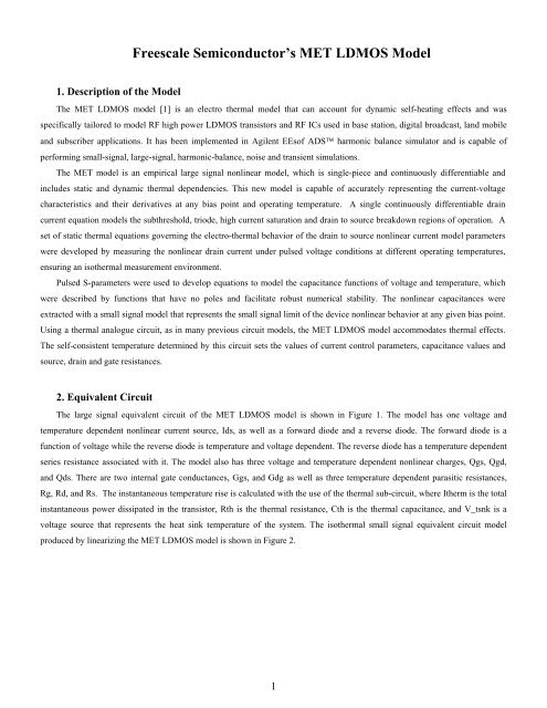
Freescale Semiconductor's MET LDMOS Model
Freescale Semiconductor's MET LDMOS Model
Freescale Semiconductor's MET LDMOS Model

You also want an ePaper? Increase the reach of your titles
YUMPU automatically turns print PDFs into web optimized ePapers that Google loves.
1. Description of the <strong>Model</strong><br />
<strong>Freescale</strong> Semiconductor’s <strong>MET</strong> <strong>LDMOS</strong> <strong>Model</strong><br />
The <strong>MET</strong> <strong>LDMOS</strong> model [1] is an electro thermal model that can account for dynamic self-heating effects and was<br />
specifically tailored to model RF high power <strong>LDMOS</strong> transistors and RF ICs used in base station, digital broadcast, land mobile<br />
and subscriber applications. It has been implemented in Agilent EEsof ADS harmonic balance simulator and is capable of<br />
performing small-signal, large-signal, harmonic-balance, noise and transient simulations.<br />
The <strong>MET</strong> model is an empirical large signal nonlinear model, which is single-piece and continuously differentiable and<br />
includes static and dynamic thermal dependencies. This new model is capable of accurately representing the current-voltage<br />
characteristics and their derivatives at any bias point and operating temperature. A single continuously differentiable drain<br />
current equation models the subthreshold, triode, high current saturation and drain to source breakdown regions of operation. A<br />
set of static thermal equations governing the electro-thermal behavior of the drain to source nonlinear current model parameters<br />
were developed by measuring the nonlinear drain current under pulsed voltage conditions at different operating temperatures,<br />
ensuring an isothermal measurement environment.<br />
Pulsed S-parameters were used to develop equations to model the capacitance functions of voltage and temperature, which<br />
were described by functions that have no poles and facilitate robust numerical stability. The nonlinear capacitances were<br />
extracted with a small signal model that represents the small signal limit of the device nonlinear behavior at any given bias point.<br />
Using a thermal analogue circuit, as in many previous circuit models, the <strong>MET</strong> <strong>LDMOS</strong> model accommodates thermal effects.<br />
The self-consistent temperature determined by this circuit sets the values of current control parameters, capacitance values and<br />
source, drain and gate resistances.<br />
2. Equivalent Circuit<br />
The large signal equivalent circuit of the <strong>MET</strong> <strong>LDMOS</strong> model is shown in Figure 1. The model has one voltage and<br />
temperature dependent nonlinear current source, Ids, as well as a forward diode and a reverse diode. The forward diode is a<br />
function of voltage while the reverse diode is temperature and voltage dependent. The reverse diode has a temperature dependent<br />
series resistance associated with it. The model also has three voltage and temperature dependent nonlinear charges, Qgs, Qgd,<br />
and Qds. There are two internal gate conductances, Ggs, and Gdg as well as three temperature dependent parasitic resistances,<br />
Rg, Rd, and Rs. The instantaneous temperature rise is calculated with the use of the thermal sub-circuit, where Itherm is the total<br />
instantaneous power dissipated in the transistor, Rth is the thermal resistance, Cth is the thermal capacitance, and V_tsnk is a<br />
voltage source that represents the heat sink temperature of the system. The isothermal small signal equivalent circuit model<br />
produced by linearizing the <strong>MET</strong> <strong>LDMOS</strong> model is shown in Figure 2.<br />
1
+ Vrg<br />
Gate<br />
Rg<br />
+<br />
Vgs<br />
Ids = f(Vds,Vgs,T) -<br />
-<br />
+<br />
-<br />
Qgs<br />
Qgd<br />
+ -<br />
+ Vgd -<br />
Gdg<br />
Ids<br />
+<br />
Vds<br />
+ Vrd -<br />
Rd<br />
Qds<br />
+<br />
-<br />
Idiode_f = f(Vds)<br />
-<br />
Idiode_r = f(Vdiode_r,T) Ggs<br />
Qds = f(Vds,T)<br />
Qgs = f(Vgs,T)<br />
Qgd = f(Vgd,T)<br />
Itherm = f(Vds,Vgs,Vgd,Vrg,Vrd,Vrs,Vdiode_r)<br />
Rs, Rd, Rg, Rdiode = f(T)<br />
Gate<br />
+<br />
Vrs<br />
-<br />
Rs<br />
Source<br />
Drain<br />
Idiode_r<br />
Rdiode<br />
Thermal<br />
Cth<br />
Itherm Rth Vth_rise<br />
+ - V_tsnk<br />
Figure 1. Large Signal Equivalent Circuit of the <strong>MET</strong> <strong>LDMOS</strong> model.<br />
Rg Cgd Gdg<br />
Rd<br />
+<br />
Vgs<br />
-<br />
Ggs<br />
Cgs<br />
+ Vgd -<br />
+<br />
Vrs<br />
-<br />
I1 I2 Cds Gds<br />
Rs<br />
Source<br />
Forward Bias (Vds>0, Gm 2 =0)<br />
-<br />
Vdiode_r<br />
+<br />
+<br />
Vds<br />
I1 = Vgs * Gm 1 * exp(-jωTAU)<br />
Reverse Bias (Vds
3. <strong>Model</strong> Parameters<br />
The following table contains all the <strong>MET</strong> <strong>LDMOS</strong> model parameter definitions and their units.<br />
PARA<strong>MET</strong>ER NAME PARA<strong>MET</strong>ER DEFINITION DEFAULT VALUE UNITS<br />
RG_0 Gate Resistance Evaluated at Tnom 1 Ω<br />
RG_1 Gate Resistance Coefficient 0.001 Ω/K<br />
RS_0 Source Resistance Evaluated at Tnom .1 Ω<br />
RS_1 Source Resistance Coefficient 0.0001 Ω/K<br />
RD_0 Drain Resistance Evaluated at Tnom 1.5 Ω<br />
RD_1 Drain Resistance Coefficient 0.0015 Ω/K<br />
VTO_0 Forward Threshold Voltage Evaluated at Tnom 3.5 V<br />
VTO_1 Forward Threshold Voltage Coefficient -0.001 V/K<br />
GAMMA IDS Equation Coefficient -0.02 ---<br />
VST Sub-Threshold Slope Coefficient 0.15 V<br />
BETA_0 IDS Equation Coefficient. BETA Evaluated at Tnom 0.2 1/Ω<br />
BETA_1 IDS Equation Coefficient -0.0002 1/(ΩK)<br />
LAMBDA IDS Equation Coefficient -0.0025 1/V<br />
VGEXP IDS Equation Coefficient 1.1 ---<br />
ALPHA IDS Equation Coefficient 1.5 ---<br />
VK IDS Equation Coefficient 7.0 V<br />
DELTA IDS Equation Coefficient 0.9 V<br />
VBR_0 Breakdown Voltage Evaluated at Tnom 75.0 V<br />
VBR_1 Breakdown Coefficient @ Vgs=0V 0.01 V/K<br />
K1 Breakdown Parameter 1.5 ---<br />
K2 Breakdown Parameter 1.15 1/V<br />
M1 Breakdown Parameter 9.5 ---<br />
M2 Breakdown Parameter 1.2 1/V<br />
M3 Breakdown Parameter 0.001 ---<br />
BR Reverse IDS Equation Coefficient 0.5 1/(VΩ)<br />
RDIODE_0 Reverse Diode Series Resistance Evaluated at Tnom .5 Ω<br />
RDIODE_1 Reverse Diode Series Resistance Coefficient 0.001 Ω/K<br />
ISR Reverse Diode Leakage Current 1e-13 A<br />
NR Reverse Diode Ideality Factor 1.0 ---<br />
VTO_R Reverse Threshold Voltage Coefficient 3.0 V<br />
RTH Thermal Resistance Coefficient 10 °C/Watts<br />
GGS Gate To Source Conductance 1e5 1/Ω<br />
GGD Gate to Drain Conductance 1e5 1/Ω<br />
TAU Transit Time Under Gate 1e-12 Seconds<br />
TNOM Temperature at Which <strong>Model</strong> Parameters are Extracted 298 K<br />
TSNK Heat Sink Temp. 25.0 °C<br />
CGST Cgs Temperature Coefficient 0.001 1/K<br />
CDST Cds Temperature Coefficient 0.001 1/K<br />
3
CGDT Cgd Temperature Coefficient 0.0 1/K<br />
CTH Thermal Capacitance 0.0 J/°C<br />
KF Flicker Noise Coefficient 0.0 ---<br />
AF Flicker Noise Exponent 1.0 ---<br />
FFE Flicker Noise Frequency Exponent 1.0 ---<br />
N Forward Diode Ideality Factor 1.0 ---<br />
ISS Forward Diode Leakage Current 1e-13 A<br />
CGS1 Cgs Equation Coefficient 2e-12 F<br />
CGS2 Cgs Equation Coefficient 1e-12 F<br />
CGS3 Cgs Equation Coefficient -4.0 V<br />
CGS4 Cgs Equation Coefficient 1e-12 F<br />
CGS5 Cgs Equation Coefficient 0.25 1/V<br />
CGS6 Cgs Equation Coefficient 3.5 1/V<br />
CGD1 Cgd Equation Coefficient 4e-13 F<br />
CGD2 Cgd Equation Coefficient 1e-13 F<br />
CGD3 Cgd Equation Coefficient 0.1 1/V 2<br />
CGD4 Cgd Equation Coefficient 4 V<br />
CDS1 Cds Equation Coefficient 1e-12 F<br />
CDS2 Cds Equation Coefficient 1.5e-12 F<br />
CDS3 Cds Equation Coefficient 0.1 1/V 2<br />
AREA Gate Periphery Scaling Parameter 1 ---<br />
N_FING Gate Finger Scaling Parameter 1 ---<br />
4. Scaling Rules<br />
The model parameters are scaled by two different parameters, AREA, which is the ratio of the desired gate periphery to the<br />
gate periphery of the transistor used in the extraction of the model parameters, and N_FING, which is the ratio of the desired<br />
number of fingers to the number of fingers of the transistor used in the extraction of the model parameters. [2]<br />
Znew<br />
AREA = (1)<br />
Zextracted<br />
NGates _ extracted<br />
N _ FING = (2)<br />
NGates _ new<br />
where Znew and Ngates_new are the gate periphery and number of gate fingers respectively of the desired transistor, and<br />
Zextracted and NGates_extracted are the gate periphery and number of gate fingers of the extracted transistor.<br />
RD _ 0<br />
RD _ 0 = (3)<br />
AREA<br />
RS _ 0<br />
RS _ 0 = (4)<br />
AREA<br />
RG _0<br />
= RG _0<br />
* AREA*<br />
N _ FING<br />
2<br />
4<br />
(5)
5. <strong>MET</strong> <strong>LDMOS</strong> <strong>Model</strong> Equations<br />
RD _ 1<br />
RD _ 1 = (6)<br />
AREA<br />
RS _ 1<br />
RS _ 1 = (7)<br />
AREA<br />
RG _ 1 = RG _ 1*<br />
AREA*<br />
N _ FING<br />
2<br />
5.1 The temperature dependency of parasitic resistances is given by:<br />
RDSO<br />
RDSO = (9)<br />
AREA<br />
GGD = GGD*<br />
AREA<br />
(10)<br />
GGS = GGS * AREA<br />
(11)<br />
RTH _0<br />
RTH _0<br />
= (12)<br />
AREA<br />
C _TH<br />
= C _TH<br />
* AREA<br />
(13)<br />
BETA _0<br />
= BETA _0<br />
* AREA<br />
(14)<br />
BETA _ 1 = BETA _ 1*<br />
AREA<br />
(15)<br />
CGS 1 = CGS1*<br />
AREA<br />
(16)<br />
CGS 2 = CGS2<br />
* AREA<br />
(17)<br />
CGS 4 = CGS4<br />
* AREA<br />
(18)<br />
CGD 1 = CGD1*<br />
AREA<br />
(19)<br />
CGD 2 = CGD2*<br />
AREA<br />
(20)<br />
CDS 1 = CDS1*<br />
AREA<br />
(21)<br />
CDS 2 = CDS2<br />
* AREA<br />
(22)<br />
ISS = ISS * AREA<br />
(23)<br />
ISR = ISR*<br />
AREA<br />
(24)<br />
BR = BR*<br />
AREA<br />
(25)<br />
RDIODE _ 0<br />
RDIODE _ 0 = (26)<br />
AREA<br />
RDIODE _1<br />
RDIODE _1<br />
= (27)<br />
AREA<br />
( T TNOM )<br />
Rg = RG _ 0 + RG _ 1*<br />
−<br />
(28)<br />
( T TNOM )<br />
Rd = RD _ 0 + RD _ 1*<br />
−<br />
(29)<br />
( T TNOM )<br />
Rs = RS _ 0 + RS _ 1*<br />
−<br />
(30)<br />
T = Vth _ rise + V _ tsnk + 273 = Vth _ rise + TSNK + 273<br />
(31)<br />
5<br />
(8)
where T is the actual or total temperature (not the temperature rise) in K and TNOM is the temperature at which the parameters<br />
were extracted. The value of V_tsnk (°C) is numerically equal to the heat sink temperature TSNK (°C). Notice that eventhough<br />
RG_1, RD_1 and RS_1 have units of Ω/K, their numerical value will be the same if the units are Ω/°C.<br />
5.2 The forward bias drain to source current equation is given by:<br />
( T TNOM )<br />
Vto _ f = VTO _ 0 + VTO _1*<br />
−<br />
(32)<br />
( T TNOM )<br />
Beta = BETA _ 0 + BETA _1<br />
* −<br />
(33)<br />
( T TNOM )<br />
Vbr = VBR _ 0 + VBR _1*<br />
−<br />
(34)<br />
To maintain small signal to large signal model consistency, the gate to source voltage used in the calculation of the large<br />
signal drain to source current is delayed TAU seconds.<br />
C)<br />
( t)<br />
= Vgs(<br />
t TAU )<br />
Vgs _ delayed −<br />
(35)<br />
( Vto _ f ( GAMMA Vds)<br />
)<br />
Vgst 2 = Vgs _ delayed − + *<br />
(36)<br />
1 ⎛<br />
2<br />
2 2<br />
2<br />
Vgst 1 = Vgst2<br />
−<br />
⎞<br />
⎜Vgst2<br />
+ ( Vgst2<br />
−VK)<br />
+ DELTA − VK + DELTA ⎟ (37)<br />
2 ⎝<br />
⎠<br />
⎛ Vgst1<br />
⎞<br />
Vgst = VST * ln⎜e<br />
VST + 1⎟<br />
(38)<br />
⎜ ⎟<br />
⎝ ⎠<br />
Vbr<br />
Vbreff = 1 −<br />
2<br />
1<br />
Vbreff1 =<br />
K2<br />
( + Tanh[<br />
M1 Vgst*<br />
M2<br />
⎛ Vds ⎞<br />
⎜<br />
⎝Vbreff<br />
⎠<br />
( ) ⎟ Vds − Vbreff + M3⎜<br />
]) (39)<br />
VGEXP<br />
⎡Vds<br />
* ALPHA⎤<br />
Vbreff1<br />
Ids = ( Beta)(<br />
Vgst )( 1 + LAMBDA*<br />
Vds)<br />
Tanh⎢<br />
⎥(<br />
1+<br />
K1*<br />
e ) (41)<br />
⎣ Vgst ⎦<br />
5.3 The forward bias drain to source diode is given by:<br />
(40)<br />
k*<br />
T<br />
Vt = (42)<br />
q<br />
where k is the Boltzmann’s constant (1.381e-23 J/K), T is the temperature in Kelvin, and q is the electron charge (1.602E-19<br />
( Vds−Vbr<br />
) ⎛ ⎞<br />
= ⎜ N*<br />
Vt<br />
Idiode _ f ISS e ⎟<br />
(43)<br />
⎜<br />
⎝<br />
6<br />
⎟<br />
⎠
5.4 The reverse bias drain to source current equation is given by:<br />
( T TNOM )<br />
Vto_r = VTO_R + VTO_1*<br />
−<br />
(44)<br />
Vgst2 = Vgs_delayed<br />
−(Vto_r<br />
−(GAMMA*<br />
Vds))<br />
(45)<br />
1 ⎛<br />
2<br />
2<br />
2<br />
2<br />
Vgst1 = Vgst2 −<br />
⎞<br />
⎜Vgst2<br />
+ (Vgst2 −VK)<br />
+ DELTA ) − VK + DELTA ⎟ (46)<br />
2 ⎝<br />
⎠<br />
5.5 The reverse bias drain to source diode is given by:<br />
⎛ Vgst1 ⎞<br />
Vgst = VST * ln⎜e<br />
VST + 1⎟<br />
(47)<br />
⎜ ⎟<br />
⎝ ⎠<br />
( BR)(<br />
Vds)(<br />
Vgst)<br />
Ids = (48)<br />
k*<br />
T<br />
Vt2 = (49)<br />
q<br />
3<br />
NR<br />
⎛ ⎛ −Eg<br />
⎞ ⎛ T ⎞ ⎞<br />
⎜ ⎜ ⎟*<br />
⎜1−<br />
⎟ ⎟<br />
⎝ ⎝ NR*<br />
Vt2 ⎠ ⎝ TNOM ⎠ ⎠<br />
⎛ T ⎞<br />
Ism = ISR*<br />
⎜ ⎟ e<br />
(50)<br />
⎝ TNOM ⎠<br />
where Eg is the energy gap for Silicon which is equal to 1.11 [3] and T is temperature in Kelvin.<br />
Idiode _ r<br />
The reverse diode's series resistance is given by:<br />
Vdiode_r ⎛ ⎞<br />
⎜ NR*<br />
Vt2<br />
= Ism*<br />
⎟<br />
⎜<br />
e −1<br />
⎟<br />
⎝ ⎠<br />
( T TNOM )<br />
Rdiode = RDIODE _ 0 + RDIODE _ 1*<br />
−<br />
(52)<br />
5.6 The gate to source capacitance equation is given by:<br />
( CGS1 + CGS2*<br />
[ + Tanh(<br />
CGS6 * ( Vgs + CGS3)<br />
) ] + CGS4*<br />
[ 1−<br />
Tanh(<br />
Vgs*<br />
CGS5)<br />
] ) * ( + CGST * (T TNOM) )<br />
Cgs = 1 1<br />
−<br />
(53)<br />
5.7 The gate to drain capacitance equation is given by:<br />
⎛<br />
CGD2 ⎞<br />
Cgd = ⎜CGD1+<br />
⎟*<br />
1<br />
−<br />
⎜ CGD3*<br />
( Vgd CGD4)<br />
⎟<br />
⎝ 1+<br />
− ⎠<br />
( + CGDT * (T TNOM)<br />
(51)<br />
2 ) (54)<br />
7
5.8 The drain to source capacitance equation is given by:<br />
⎛<br />
CDS2 ⎞<br />
Cds = ⎜CDS1<br />
+<br />
⎟*<br />
1<br />
−<br />
⎝ 1 + CDS3*<br />
Vds ⎠<br />
( + CDST * (T TNOM)<br />
2 ) (55)<br />
5.9 The noise is calculated as shown in [3], as the sum of the thermal chanel noise and the flicker noise as shown by the<br />
following equation:<br />
⎛<br />
2 8*<br />
k * T * g m<br />
=<br />
+ ⎜<br />
Ids<br />
id KF *<br />
3<br />
⎜<br />
⎝ f<br />
where gm is the transconductance of the device at the operating point, T is temperature in Kelvin, and f is the frequency. In<br />
addition all resistors are also modeled as thermal noise sources.<br />
4*<br />
k * T<br />
R<br />
where R is the resistance value and T is the temperature in Kelvin.<br />
AF<br />
FFE<br />
⎞<br />
⎟<br />
⎠<br />
(56)<br />
2<br />
id R = (57)<br />
5.10 To avoid convergence problems the maximum temperature rise, Vth_rise (°C) is limited to 300 °C using the following<br />
equation:<br />
6. References<br />
⎧<br />
⎪<br />
⎪<br />
0<br />
Vth _ rise = ⎨ Vth _ rise<br />
⎪<br />
⎪<br />
⎡Vth_rise − 250⎤<br />
250 + 50*<br />
tanh<br />
⎪<br />
⎢<br />
⎥<br />
⎩<br />
⎣ 50 ⎦<br />
0 ≤ Vth _ rise<br />
0 < Vth _ rise < 250<br />
250 ≤ Vth _ rise<br />
(58)<br />
[1] W. Curtice, J. Plá, D. Bridges, T. Liang & E. Shumate, A New Dynamic Electro-Thermal Nonlinear <strong>Model</strong> for Silicon<br />
RF<br />
<strong>LDMOS</strong> FETs, 1999 IEEE MTT-S International Microwave Symposium, Anaheim CA, pp. 419-422<br />
[2] M. Golio, Microwave MESFETs and HEMTs, Arthec House, Boston, 1991, pp. 79-80<br />
[3] P. Antognetti & G. Massobrio, Semiconductor Device <strong>Model</strong>ing with SPICE, McGraw Hill, New York, 1988.<br />
8


