

Integration of SiCN as a Low k Etch Stop and Cu Passivation in a ...
Integration of SiCN as a Low k Etch Stop and Cu Passivation in a ...
Integration of SiCN as a Low k Etch Stop and Cu Passivation in a ...

You also want an ePaper? Increase the reach of your titles
YUMPU automatically turns print PDFs into web optimized ePapers that Google loves.
<strong>Integration</strong> <strong>of</strong> <strong>SiCN</strong> <strong>as</strong> a <strong>Low</strong> k <strong>Etch</strong> <strong>Stop</strong> <strong>and</strong> <strong>Cu</strong> P<strong>as</strong>sivation <strong>in</strong> a High Performance<br />
<strong>Cu</strong>/<strong>Low</strong> k Interconnect<br />
Jeremy Mart<strong>in</strong>, a) Stan Filipiak, b) Tab Stephens, b) Fred Huang, b) M<strong>as</strong>sud Am<strong>in</strong>pur, a) Judith Mueller b)<br />
Ertugrul Demircan, b) Larry Zhao, a) Jim Werk<strong>in</strong>g, a) C<strong>in</strong>dy Goldberg, b) Steve Park, a) Terry Sparks, b)<br />
Christ<strong>in</strong>e Esber, a)<br />
a) Advanced Micro Devices, AMD/Motorola Alliance, 3501 Ed Blueste<strong>in</strong> Blvd., Aust<strong>in</strong>, TX 78721<br />
b) Motorola, Dan Noble Center, 3501 Ed Blueste<strong>in</strong> Blvd., Aust<strong>in</strong>, TX 78721<br />
Abstract<br />
This paper describes the <strong>in</strong>tegration <strong>of</strong> a silicon<br />
carbon nitride (<strong>SiCN</strong>) copper p<strong>as</strong>sivation <strong>and</strong> etch stop layer<br />
<strong>in</strong>to a <strong>Cu</strong> low k dielectric <strong>in</strong>terconnect technology. The <strong>in</strong>corporation<br />
<strong>of</strong> <strong>SiCN</strong> improves <strong>in</strong>terconnect performance by<br />
virtue <strong>of</strong> its lower dielectric constant <strong>as</strong> compared to silicon<br />
nitride, <strong>and</strong> through changes to the process <strong>in</strong>tegration made<br />
possible by the improved etch selectivity <strong>and</strong> good copper<br />
<strong>in</strong>terface properties.<br />
Introduction<br />
The need to reduce circuit delay time due to the <strong>in</strong>terconnect<br />
<strong>as</strong> technology scales to smaller dimensions is<br />
well known (1). The two pr<strong>in</strong>cipal approaches to this problem<br />
are reduction <strong>of</strong> the resistance through use <strong>of</strong> <strong>Cu</strong> metallization,<br />
<strong>and</strong> reduction <strong>of</strong> capacitance through the use <strong>of</strong><br />
lower dielectrics constant (κ) materials. The most prom<strong>in</strong>ent<br />
changes to dielectric materials are the use <strong>of</strong> new low κ <strong>in</strong>ter-<br />
<strong>and</strong> <strong>in</strong>tra-layer dielectrics (ILDs) (2). For example,<br />
PECVD SiCOH (also know <strong>as</strong> organosilicate gl<strong>as</strong>s or OSG)<br />
films or other low κ films have been used <strong>in</strong> place <strong>of</strong> SiO2 or<br />
Fluor<strong>in</strong>e doped SiO2 (FSG) (3). Changes to other dielectric<br />
materials such <strong>as</strong> etch stop layers <strong>and</strong> <strong>Cu</strong> p<strong>as</strong>sivation layers<br />
can also improve <strong>in</strong>terconnect performance used either <strong>in</strong><br />
conjunction with SiO2 or FSG dielectrics (4), or together<br />
with low k dielectrics (5).<br />
Inlaid <strong>Cu</strong> process technologies (also called dam<strong>as</strong>cene)<br />
have generally used silicon nitride (SiN) <strong>as</strong> <strong>Cu</strong> p<strong>as</strong>sivation<br />
<strong>and</strong> etch stop layers (ESL). However, because the<br />
dielectric constant <strong>of</strong> SiN is nearly double that <strong>of</strong> FSG <strong>and</strong><br />
more than double that <strong>of</strong> low κ films, it contributes disproportionately<br />
to the effective κ value <strong>of</strong> the dielectric stack.<br />
<strong>Integration</strong> schemes that require a thick SiN layer lose much<br />
<strong>of</strong> the benefit <strong>of</strong> the low κ ILD. For SiCOH ILDs the problem<br />
is exacerbated by poor etch selectivity between SiCOH<br />
<strong>and</strong> SiN, relative to SiO2 or FSG <strong>and</strong> SiN. Due to the poor<br />
etch selectivity a thicker SiN layer is required to achieve<br />
etch performance with SiCOH that is equivalent to SiO2 or<br />
FSG. The problems <strong>as</strong>sociated with SiN ESL can be mitigated<br />
by the use <strong>of</strong> an alternate material. <strong>SiCN</strong>, <strong>in</strong> particular,<br />
is an attractive replacement for SiN <strong>as</strong> both an ESL <strong>and</strong><br />
<strong>Cu</strong> p<strong>as</strong>sivation film. <strong>SiCN</strong> h<strong>as</strong> a dielectric constant approximately<br />
25% lower than SiN. <strong>SiCN</strong> also shows sub-<br />
stantially improved selectivity compared to SiN <strong>in</strong> SiCOH<br />
etch processes, while ma<strong>in</strong>ta<strong>in</strong><strong>in</strong>g good etch characteristics<br />
<strong>in</strong> etch processes developed to etch <strong>SiCN</strong>. In addition, <strong>SiCN</strong><br />
h<strong>as</strong> excellent performance <strong>as</strong> a <strong>Cu</strong> p<strong>as</strong>sivation layer <strong>in</strong> terms<br />
<strong>of</strong> electromigration <strong>and</strong> copper hillock density.<br />
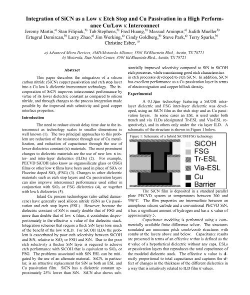
Experimental<br />
A 0.13μm technology featur<strong>in</strong>g a SiCOH <strong>in</strong>tralayer<br />
dielectric <strong>and</strong> FSG <strong>in</strong>ter-layer dielectric w<strong>as</strong> developed,<br />
us<strong>in</strong>g an <strong>SiCN</strong> film <strong>as</strong> the etch stop <strong>and</strong> <strong>as</strong> <strong>Cu</strong> p<strong>as</strong>sivation<br />
layers. In some c<strong>as</strong>es an ESL is used under both<br />
trench <strong>and</strong> via ILDs (designated Tr-ESL <strong>and</strong> Via-ESL respectively),<br />
<strong>and</strong> <strong>in</strong> others only under the via layer ILD. A<br />
schematic <strong>of</strong> the structure is shown <strong>in</strong> Figure 1 below.<br />
Figure 1: Schematic <strong>of</strong> a hybrid SiCOH/FSG technology<br />
The <strong>SiCN</strong> film is deposited <strong>in</strong> a st<strong>and</strong>ard parallel<br />
plate PECVD system at temperatures between 300 <strong>and</strong><br />
350°C. The film properties are <strong>in</strong>termediate between an<br />
amorphous silicon carbide <strong>and</strong> a conventional PECVD SiN,<br />
it h<strong>as</strong> a significant amount <strong>of</strong> hydrogen <strong>and</strong> h<strong>as</strong> a κ value <strong>of</strong><br />
approximately 5.<br />
Capacitance model<strong>in</strong>g is performed us<strong>in</strong>g a commercially<br />
available f<strong>in</strong>ite difference solver. The structures<br />
simulated are m<strong>in</strong>imum pitch comb/comb structures with<br />
combs at the layers above <strong>and</strong> below. Capacitance results<br />
are presented <strong>in</strong> terms <strong>of</strong> an effective κ that is def<strong>in</strong>ed <strong>as</strong> the<br />
κ value <strong>of</strong> a hypothetical dielectric without any caps, ESLs<br />
or p<strong>as</strong>sivation layers that reproduces the total capacitance <strong>of</strong><br />
the modeled dielectric stack. The effective κ value is directly<br />
proportional to total capacitance <strong>and</strong> captures the effect<br />
<strong>of</strong> changes <strong>in</strong> the thickness <strong>of</strong> the different dielectrics <strong>in</strong><br />
a way that is <strong>in</strong>tuitively related to ILD film κ values.
Results <strong>and</strong> Discussion<br />
Implementation <strong>of</strong> an <strong>SiCN</strong> ESL reduces capacitance directly<br />
because its dielectric constant is lower than SiN (approximately<br />
5 for <strong>SiCN</strong> versus approximately 7 for SiN).<br />
The effect <strong>of</strong> ESL thickness <strong>and</strong> material on κ effective is<br />
shown <strong>in</strong> Table 1.<br />
Table 1. Simulation data show<strong>in</strong>g the effect <strong>of</strong> trench <strong>and</strong> via<br />
ESL thickness <strong>and</strong> material on the effective dielectric constant<br />
<strong>of</strong> the stack<br />
ILD Ma- ESL Tr-ESL Via ESL K eff<br />
terial<br />
Thickness<br />
Thickness<br />
FSG SiN 300A 300A 4.21<br />
FSG SiN 500A 500A 4.44<br />
SiCOH SiN 300A 300A 3.86<br />
SiCOH SiN 500A 500A 4.12<br />
SiCOH SiN 700A 700A 4.35<br />
SiCOH SiN 0A 300A 3.62<br />
SiCOH SiN 0A 500A 3.73<br />
SiCOH SiN 0A 700A 3.81<br />
SiCOH SiN 0A 900A 3.87<br />
SiCOH <strong>SiCN</strong> 300A 300A 3.62<br />
SiCOH <strong>SiCN</strong> 500A 500A 3.74<br />
SiCOH <strong>SiCN</strong> 700A 700A 3.86<br />
SiCOH <strong>SiCN</strong> 0A 300A 3.50<br />
SiCOH <strong>SiCN</strong> 0A 500A 3.54<br />
SiCOH <strong>SiCN</strong> 0A 700A 3.57<br />
It will be observed that the effective κ value <strong>of</strong> the<br />
dielectric stack is dramatically affected by the thickness <strong>of</strong><br />
the ESL. If the ESL thickness is held constant while the<br />
material is changed from SiN to <strong>SiCN</strong> the κ effective will be<br />
reduced by 6%, 9% <strong>and</strong> 11% for 300A, 500A, <strong>and</strong> 700A<br />
ESLs at both trench <strong>and</strong> via, respectively.<br />
Figure 2 shows the me<strong>as</strong>ured total capacitance<br />
plotted versus resistance for a 300A <strong>and</strong> 500A <strong>SiCN</strong> <strong>and</strong> a<br />
300A SiN. Fitt<strong>in</strong>g a l<strong>in</strong>e to the distributions for each ESL<br />
<strong>and</strong> compar<strong>in</strong>g their values at relative resistance value <strong>of</strong> 1<br />
shows a 6.3% capacitance improvement <strong>in</strong> the 300A <strong>SiCN</strong><br />
Figure 2: Total Capacitance versus Resistance<br />
Relative Capacitance (arbitrary units)<br />
1.1<br />
1<br />
.85 .9 .95 1 1.05 1.1 1.15 1.2<br />
Relative Resistance (arbitrarty units)<br />
(th<strong>in</strong> solid l<strong>in</strong>e) versus 300A SiN (thick solid l<strong>in</strong>e), <strong>and</strong> a<br />
4.5% improvement compar<strong>in</strong>g 500A <strong>SiCN</strong> (d<strong>as</strong>hed l<strong>in</strong>e) to<br />
300A SiN. These values are consistent with the 6% <strong>and</strong> 3%<br />
κ effective reductions predicted <strong>in</strong> Table 1, <strong>and</strong> are confirmed<br />
by more detailed statistical analysis <strong>of</strong> this <strong>and</strong> other<br />
data. The larger than predicted improvement for the 500A<br />
<strong>SiCN</strong> is attributable to the <strong>in</strong>cre<strong>as</strong>e <strong>in</strong> the <strong>in</strong>terlayer spac<strong>in</strong>g<br />
when the ESL thickness is <strong>in</strong>cre<strong>as</strong>ed. For simplicity <strong>of</strong><br />
comparison the layer to layer spac<strong>in</strong>g w<strong>as</strong> held constant <strong>in</strong><br />
the simulations shown <strong>in</strong> Table 1.<br />
In addition to the direct improvements to κ effective<br />
obta<strong>in</strong>ed by switch<strong>in</strong>g to a lower κ ESL, there are <strong>in</strong>direct<br />
benefits result<strong>in</strong>g from the improved etch performance<br />
<strong>of</strong> <strong>SiCN</strong>, especially when it used <strong>in</strong> conjunction with SiCOH<br />
ILDs. Replac<strong>in</strong>g SiO2 or FSG with SiCOH requires new<br />
etch processes that generally have substantially lower<br />
SiN/SiCOH selectivity than the SiN/SiO2 or SiN/FSG selectivities<br />
<strong>in</strong> the orig<strong>in</strong>al processes. Replac<strong>in</strong>g the SiN with<br />
<strong>SiCN</strong> restores some <strong>of</strong> the lost etch selectivity, which benefits<br />
the overall <strong>in</strong>tegration.<br />
Figure 3 shows cross sections compar<strong>in</strong>g structures<br />
built with a 500A <strong>SiCN</strong> ESL to 300A SiN ESL used at both<br />
trench <strong>and</strong> via. Even with this <strong>in</strong>cre<strong>as</strong>e <strong>in</strong> the <strong>SiCN</strong> ESL<br />
thickness, the κ effective performance is still improved.<br />
Moreover, the etch performance <strong>of</strong> the stack is improved.<br />
The overetch <strong>of</strong> the trench <strong>in</strong>to the underly<strong>in</strong>g via dielectric<br />
is reduced <strong>and</strong> the trench bottom pr<strong>of</strong>ile is more controlled.<br />
The <strong>in</strong>tegration benefits <strong>as</strong>sociated with the improved<br />
selectivity <strong>of</strong> <strong>SiCN</strong>/SiCOH versus SiN/SiCOH become<br />
even more critical for more challeng<strong>in</strong>g etch processes<br />
such <strong>as</strong> a stop on ESL via etch <strong>in</strong> a via first dual <strong>in</strong>laid <strong>in</strong>tegration<br />
scheme. Figure 4 shows a set <strong>of</strong> SEM images <strong>of</strong> a<br />
dual <strong>in</strong>laid via etch process for a SiCOH trench ILD <strong>and</strong> an<br />
FSG via ILD with no trench ESL. The requirement for the<br />
etch process is to stop on the via ESL without expos<strong>in</strong>g <strong>Cu</strong><br />
<strong>in</strong> any features across the wafer. The results <strong>in</strong> Figure 4<br />
illustrate the effective etch selectivity by show<strong>in</strong>g the ESL<br />
removal <strong>in</strong> structures <strong>of</strong> widely vary<strong>in</strong>g etch rates. The ex-<br />
Figure 3: SEM Cross sections compar<strong>in</strong>g structures with 500A<br />
<strong>SiCN</strong> (left) <strong>and</strong> 300A SiN (right)
Figure 4: Enhanced etch selectivity <strong>of</strong> <strong>SiCN</strong> versus SiN for a<br />
dual <strong>in</strong>laid via etch<br />
treme slow etch<strong>in</strong>g feature (a center via) is shown on the left<br />
<strong>and</strong> the f<strong>as</strong>t etch<strong>in</strong>g feature (an edge die seal) is shown on<br />
the right. The via etch depth w<strong>as</strong> set to ensure the center<br />
vi<strong>as</strong> opened, <strong>and</strong> the figure <strong>in</strong>dicates the me<strong>as</strong>ured ESL loss<br />
<strong>in</strong> the edge die seal. In order to avoid expos<strong>in</strong>g <strong>Cu</strong>, the ESL<br />
thickness must be sufficiently greater than the observed loss.<br />
For a 25% marg<strong>in</strong>, approximately 500A <strong>of</strong> <strong>SiCN</strong> would be<br />
required, while nearly 900A <strong>of</strong> SiN would be required to<br />
achieve the same result. Referr<strong>in</strong>g back to Table 1, we see<br />
that this will lead to a κ effective <strong>of</strong> 3.54 for the <strong>SiCN</strong> c<strong>as</strong>e,<br />
<strong>and</strong> 3.87 for the SiN c<strong>as</strong>e, an 8.5% improvement for the<br />
<strong>SiCN</strong> c<strong>as</strong>e.<br />
In addition to the improvements <strong>in</strong> etch behavior<br />
<strong>and</strong> capacitance reduction, us<strong>in</strong>g <strong>SiCN</strong> <strong>in</strong> a low κ <strong>in</strong>terconnect<br />
structure leads to improved <strong>Cu</strong> p<strong>as</strong>sivation performance.<br />
Figure 5 compares the electromigration performance<br />
<strong>of</strong> <strong>SiCN</strong> with <strong>and</strong> without a pl<strong>as</strong>ma pretreatment <strong>and</strong> SiN.<br />
The <strong>SiCN</strong> without a pretreatment performs comparably to<br />
the b<strong>as</strong>el<strong>in</strong>e SiN split. However, the <strong>SiCN</strong> split with the<br />
pretreatment substantially outperforms the SiN, with higher<br />
Median Time to Failure (MTTF). This split also h<strong>as</strong> a<br />
higher activation energy (6). The pretreatment modifies the<br />
<strong>Cu</strong> <strong>SiCN</strong> <strong>in</strong>terface, lead<strong>in</strong>g to excellent adhesion <strong>and</strong> reduced<br />
<strong>Cu</strong>O at the <strong>Cu</strong>/<strong>SiCN</strong> <strong>in</strong>terface. More detailed analysis<br />
<strong>of</strong> the effects <strong>of</strong> these treatments on the <strong>Cu</strong>/<strong>SiCN</strong> <strong>in</strong>terface<br />
may be addressed <strong>in</strong> a future publications.<br />
Pl<strong>as</strong>ma pretreatments can sometimes lead to a high<br />
density <strong>of</strong> <strong>Cu</strong> hillocks (5). These hillocks are undesirable<br />
because they <strong>in</strong>terfere with defect <strong>in</strong>spections <strong>and</strong> may lead<br />
to reliability or <strong>in</strong>tegration issues. With SiN <strong>Cu</strong> p<strong>as</strong>sivation<br />
layers, the density <strong>and</strong> size <strong>of</strong> the <strong>Cu</strong> hillocks grow rapidly<br />
<strong>as</strong> treatment conditions get more severe <strong>and</strong> treatment times<br />
are <strong>in</strong>cre<strong>as</strong>ed, <strong>and</strong> this poses a limitation on the treatment<br />
conditions that can practically be implemented. Because the<br />
deposition temperature <strong>of</strong> the <strong>SiCN</strong> (300-350°C) is lower<br />
than SiN (400°C), the density <strong>of</strong> <strong>Cu</strong> hillocks is substantially<br />
Figure 5: Reliability data for <strong>SiCN</strong><br />
Percent<br />
99.99<br />
99.9<br />
99<br />
95<br />
90<br />
80<br />
70<br />
50<br />
30<br />
20<br />
10<br />
5<br />
1<br />
reduced. Automated optical defectivity <strong>in</strong>spection shows a<br />
20X reduction <strong>in</strong> <strong>Cu</strong> hillock density for <strong>SiCN</strong> versus SiN<br />
where both films received pretreatments. AFM me<strong>as</strong>urements<br />
also show dramatic reduction <strong>in</strong> the size <strong>of</strong> the hillocks.<br />
The lower tendency toward hillock formation allows<br />
more flexibility <strong>in</strong> the optimization <strong>of</strong> pretreatments than<br />
SiN p<strong>as</strong>sivation allows.<br />
Conclusions<br />
10 100 1000 10 4<br />
.1<br />
.01<br />
The use <strong>of</strong> <strong>SiCN</strong> <strong>as</strong> a low κ etch stop <strong>and</strong> <strong>Cu</strong> p<strong>as</strong>sivation<br />
layer provides significant improvements to the performance<br />
<strong>of</strong> a <strong>Cu</strong>/SiCOH <strong>in</strong>terconnect s, with a 25% lower κ<br />
value compared to SiN. Additional benefits come from the<br />
improved etch selectivity, which enhances the manufacturability<br />
<strong>of</strong> etch processes <strong>and</strong> enables the use <strong>of</strong> th<strong>in</strong>ner etch<br />
stop layers, further reduc<strong>in</strong>g the capacitance. The <strong>Cu</strong> p<strong>as</strong>sivation<br />
properties <strong>of</strong> the <strong>SiCN</strong>/<strong>Cu</strong> <strong>in</strong>terface are also excellent.<br />
With appropriate pl<strong>as</strong>ma pretreatments excellent electromigration<br />
performance is observed, <strong>and</strong> the reduced deposition<br />
temperature suppresses <strong>Cu</strong> hillocks compared to SiN.<br />
Acknowledgements<br />
Normalized Time to Failure<br />
We gratefully acknowledge the staff at Motorola's Dan Noble<br />
Center.<br />
References<br />
SiN<br />
<strong>SiCN</strong> no treat<br />
<strong>SiCN</strong> w/ treat<br />
1. International Technology Roadmap for Semiconductors,<br />
2001<br />
2. W.W. Lee <strong>and</strong> P.S. Ho, MRS Bullet<strong>in</strong> Vol. 22, p. 19<br />
(1997).<br />
3. Aoki, H., et al., IEDM Tech. Digest, (2001)<br />
4. Sleight, J. W., et al., IEDM Tech. Digest, (2001)<br />
5. Shannon, V., Solid State Technology, Sept., S22 (2001)<br />
6. Unpublished results.


