MAC71x6 Microcontroller Device Mask Set Errata - Freescale
MAC71x6 Microcontroller Device Mask Set Errata - Freescale
MAC71x6 Microcontroller Device Mask Set Errata - Freescale
You also want an ePaper? Increase the reach of your titles
YUMPU automatically turns print PDFs into web optimized ePapers that Google loves.
<strong>Freescale</strong> Semiconductor<br />
<strong>Mask</strong> <strong>Set</strong> <strong>Errata</strong><br />
1 Introduction<br />
This document contains information on a new product. Specifications and information herein<br />
are subject to change without notice.<br />
© <strong>Freescale</strong> Semiconductor, Inc., 2004–2005. All rights reserved.<br />
• Preliminary<br />
MAC7106MSE1<br />
Rev. 1, 04/2005<br />
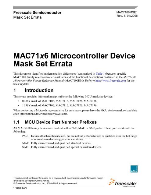
<strong>MAC71x6</strong> <strong>Microcontroller</strong> <strong>Device</strong><br />
<strong>Mask</strong> <strong>Set</strong> <strong>Errata</strong><br />
This document identifies implementation differences (summarized in Table 1) between specific<br />
MAC7100 family microcontroller mask sets and the functional descriptions contained in the MAC7100<br />
<strong>Microcontroller</strong> Family Reference Manual (MAC7100RM). Refer to http://www.freescale.com for the<br />
latest updates.<br />
This errata provides information applicable to the following MCU mask set devices:<br />
• 0L38Y mask of MAC7106, MAC7116, MAC7126, MAC7136<br />
• 1L38Y mask of MAC7106, MAC7116, MAC7126, MAC7136<br />
When contacting a Motorola representative for assistance, please have the MCU device mask set and date<br />
code information (described below) available.<br />
1.1 MCU <strong>Device</strong> Part Number Prefixes<br />
All MAC7100 family devices are marked with a PAC, MAC or SAC prefix. These prefixes denote the<br />
following:<br />
PAC <strong>Device</strong>s that have been tested, but are not fully characterized or qualified over the full range<br />
of normal manufacturing process variations.<br />
MAC Fully characterized and qualified standard devices.<br />
SAC Fully characterized and qualified special or custom devices.
<strong>Errata</strong> Summary<br />
1.2 MCU <strong>Device</strong> <strong>Mask</strong> <strong>Set</strong> Identification<br />
The mask set of a device is identified by a four-character code consisting of a letter, two numerical digits,<br />
and a letter, for example L38Y. Slight variations to the mask set identification code may result in an<br />
optional numerical digit preceding the standard four-character code, for example 0L38Y.<br />
1.3 MCU <strong>Device</strong> Date Codes<br />
In addition to the part number and mask set markings, each device is marked to indicate the week of<br />
manufacture. The date is coded as four numerical digits where the first two digits indicate the year and the<br />
last two digits indicate the work week. For example, the date code “0412” indicates that the device was<br />
manufactured during the 12th week of the year 2004.<br />
1.4 <strong>Errata</strong> System Tracking Numbers<br />
MUCts0xxxx is the tracking number for MAC7100 family device errata. An errata number can be used<br />
with the mask set and date code to identify a specific errata to a Motorola representative.<br />
2 <strong>Errata</strong> Summary<br />
2<br />
<strong>Errata</strong><br />
Number<br />
Table 1. Summary of <strong>MAC71x6</strong> <strong>Mask</strong> <strong>Set</strong> <strong>Errata</strong><br />
<strong>MAC71x6</strong> <strong>Microcontroller</strong> <strong>Device</strong> <strong>Mask</strong> <strong>Set</strong> <strong>Errata</strong>, Rev. 1<br />
Preliminary<br />
Module(s)<br />
Affected<br />
<strong>Mask</strong> <strong>Set</strong><br />
Affected<br />
Brief Description<br />
0L38Y 1L38Y<br />
MUCts01793 IPM/IPWM Modes, Value Read From UCAn May Be Incorrect eMIOS Yes Yes<br />
MUCts01831 Deactivating A Receive MB May Corrupt Another Active Receive MB FlexCAN Yes Yes<br />
MUCts01856 Changing CTARs Between Frames in Continuous PCS Mode May Cause Error DSPI Yes Yes<br />
MUCts01915 Clock Monitor Reset Causes System Lock-up CRG Yes Yes<br />
MUCts01916 VREG High Temperature Control Register (VREGHTCL) For Factory Use Only VREG Yes Yes<br />
MUCts01917 eMIOS Buffered Modes Not Available eMIOS Yes Yes<br />
MUCts02084 MCM Reset Status Register (MRSR) Always Reads 0x80 MCM Yes Yes<br />
MUCts02468 Flash Controller Returns Incorrect Data On Certain Read Accesses CFM Yes —<br />
MUCts02523 FlexCAN Transmit Buffers May Freeze or Indicate Missing Frame FlexCAN Yes Yes<br />
MUCts02527 Debug Status Port Mode 2 Incorrect Signal Assignments in Documentation SSM Yes Yes<br />
<strong>Freescale</strong> Semiconductor
3 <strong>Errata</strong> Details<br />
<strong>MAC71x6</strong> <strong>Microcontroller</strong> <strong>Device</strong> <strong>Mask</strong> <strong>Set</strong> <strong>Errata</strong>, Rev. 1<br />
<strong>Errata</strong> Details<br />
This section provides a detailed description of each errata and a description of a possible work-around,<br />
where appropriate.<br />
3.1 MUCts01793 — IPM/IPWM Modes, Value Read From<br />
UCAn May Be Incorrect<br />
Description<br />
When reading the UCAn register in Input Pulse Width Measurement (IPWM) or Input Period<br />
Measurement (IPM) modes, if the IPS bus cycle starts on the same clock cycle as an A2 capture, the data<br />
read will not be coherent with the one at the next UCBn read.<br />
• In IPWM mode, data read from UCBn will be greater than UCAn (UCBn minus UCAn will be the<br />
pulse width measurement of the polarity opposite that defined by EDPOL).<br />
• In IPM mode, data read from UCAn and UCBn will be the same.<br />
The expected scenario is that UCAn will be greater than UCBn for both modes. Note that coherency is<br />
guaranteed in a sequence of several measurements only if the combined UCAn / UCBn reads for each new<br />
measurement are performed after the correspondent new flag event.<br />
Work-Around<br />
After reading UCAn and UCBn, if UCAn is not greater than UCBn, discard this pulse measurement and<br />
read both registers again in the usual order: first read UCAn, then read UCBn.<br />
3.2 MUCts01831 — Deactivating A Receive MB May<br />
Corrupt Another Active Receive MB<br />
Description<br />
Deactivating a FlexCAN receive message buffer (MB) may cause corruption of another active receive MB<br />
if the following sequence occurs:<br />
1. A receive MB is locked via reading the Control/Status word, and has a pending message in the<br />
temporary receive serial message buffer (SMB).<br />
2. A message is received that matches a second receive MB, and is queued in the second SMB.<br />
3. The first MB is unlocked during the time between the CRC field and the 6th bit of EOF.<br />
4. The second MB is deactivated within 9 fIPS clock cycles of the first MB being unlocked, resulting<br />
in corruption of the first MB.<br />
<strong>Freescale</strong> Semiconductor Preliminary<br />
3
<strong>Errata</strong> Details<br />
Work-Around<br />
Do not write to the Control/Status word after initializing a receive MB, and use the IFLAG status bit to<br />
determine reception of a new frame, as the Control/Status field will always indicate FULL or OVERRUN<br />
after receiving the first frame.<br />
If a write (deactivation) is required to the Control/Status field of an active receive MB, a delay of 25 CAN<br />
bit times plus 9 fIPS clock cycles between unlocking one MB and deactivating another MB will avoid<br />
corruption, however frames may still be lost.<br />
3.3 MUCts01856 — Changing CTARs Between Frames in<br />
Continuous PCS Mode May Cause Error<br />
Description<br />
Under some conditions in continuous operation mode (CONT = 1), the command word associated with the<br />
data frame is not always executed properly. An incorrect transfer may occur when multiple frames are<br />
transferred in continuous PCS mode and the frames use different CTAR registers. For example, if an<br />
application tries to transmit a 12-bit frame and a 16-bit frame without negating PCS, two 12-bit frames are<br />
transferred. This has been observed in simulations where CPHA = 0. The two frames are transmitted<br />
correctly if CPHA = 1.<br />
Work-Around<br />
When CPHA = 0 and continuous PCS mode is used, extended length (> 16 bits) frames may be created<br />
only by using two frames of equal size. This means that certain frame sizes cannot be constructed (prime<br />
numbers > 16).<br />
3.4 MUCts01915 — Clock Monitor Reset Causes System<br />
Lock-up<br />
Description<br />
If the clock monitor reset function is enabled and a clock monitor time-out occurs, the chip will be placed<br />
into a reset state, but it will never exit that state. In order to trigger this errata all of the following conditions<br />
must be true:<br />
• Clock monitor is enabled (CRG PLLCTL[CME] = 0b1)<br />
• Loss of clock is detected<br />
• Self-clock mode is disabled (CRG PLLCTL[SCME] = 0b0)<br />
The only way to recover from this error is via an external or low-voltage reset sequence.<br />
4<br />
<strong>MAC71x6</strong> <strong>Microcontroller</strong> <strong>Device</strong> <strong>Mask</strong> <strong>Set</strong> <strong>Errata</strong>, Rev. 1<br />
Preliminary<br />
<strong>Freescale</strong> Semiconductor
Work-Around<br />
<strong>MAC71x6</strong> <strong>Microcontroller</strong> <strong>Device</strong> <strong>Mask</strong> <strong>Set</strong> <strong>Errata</strong>, Rev. 1<br />
<strong>Errata</strong> Details<br />
The default values of the CRG PLLCTL[CME] and PLLCTL[SCME] bits are 0b1, and thus the error is<br />
avoided if the clock monitor reset mode is never enabled. In order to prevent inadvertent enabling of the<br />
clock monitor reset function, PLLCTL[SCME] should be written with 0b1 during the first write to the<br />
PLLCTL register following a reset. Since the PLLCTL[SCME] bit is write once, this will prevent the<br />
enabling of clock monitor reset.<br />
There is no plan to correct this function, as will be reflected in future revisions of the MAC7100<br />
<strong>Microcontroller</strong> Family Reference Manual (MAC7100RM).<br />
3.5 MUCts01916 — VREG High Temperature Control<br />
Register (VREGHTCL) For Factory Use Only<br />
Description<br />
Although information describing the VREGHTCL register is included in the MAC7100 <strong>Microcontroller</strong><br />
Family Reference Manual (MAC7100RM) revisions 0.6, 0.6.1 and 1.0, the functions provided by this<br />
register are not fully characterized for customer use. Thus, VREGHTCL is reserved for factory testing<br />
during manufacturing processes, and is not suitable for application use.<br />
Work-Around<br />
There is no work-around available, nor are there plans to characterize this circuitry for customer use.<br />
Future versions of the MAC7100RM will remove the descriptions of the high temperature functions.<br />
3.6 MUCts01917 — eMIOS Buffered Modes Not Available<br />
Description<br />
Table 20-9 and Sections 20.6.7.15 through 20.6.7.18 of the MAC7100 <strong>Microcontroller</strong> Family Reference<br />
Manual (MAC7100RM) revision 1.0, describe four buffered UC modes which are implemented on other<br />
<strong>Freescale</strong> devices, but are not available on any MAC7100 family devices. The described, unavailable UC<br />
modes are:<br />
• Modulus Counter, Buffered (MCB)<br />
• Output Pulse Width and Frequency Modulation, Buffered (OPWFMB)<br />
• Center Aligned Output Pulse Width Modulation, Buffered (OPWMCB)<br />
• Output Pulse Width Modulation, Buffered (OPWMB)<br />
Work-Around<br />
The UCCRn[MODE] field should not be set to 0b1010000 through 0b1100010 (refer to Table 20-9).<br />
Future revisions of the MAC7100 <strong>Microcontroller</strong> Family Reference Manual (MAC7100RM) will remove<br />
descriptions of these UC modes.<br />
<strong>Freescale</strong> Semiconductor Preliminary<br />
5
<strong>Errata</strong> Details<br />
3.7 MUCts02084 — MCM Reset Status Register (MRSR)<br />
Always Reads 0x80<br />
Description<br />
The reset status register (MRSR) in the MCM module, which is intended to provide a read-only status of<br />
the last reset event, returns an incorrect status. In particular, the functionality of the MRSR reporting is<br />
limited such that all reset events are reported as power-on resets, regardless of the actual source of the reset.<br />
As a result, all reads of the MRSR return a data value of 0x80.<br />
Work-Around<br />
There is no work-around available.<br />
3.8 MUCts02468 — Flash Controller Returns Incorrect<br />
Data On Certain Read Accesses<br />
Description<br />
On <strong>MAC71x6</strong> devices, the Flash requires two cycles to return data on a read. For improved instruction<br />
execution performance, the Flash controller performs speculative reads such that in many cases the Flash<br />
has begun fetching the data before it is requested. Due to this mechanism the read data can be returned to<br />
the CPU with no wait states.<br />
In cases where a new read request arrives for the upper half (0x0008_0000 to 0x000F_FFFF) while a<br />
speculative read is in progress to the lower half (0x0000_0000 to 0x0007_FFFF), the speculative<br />
access is not properly cancelled and the lower half data may be returned instead of the expected data.<br />
Work-Around<br />
Avoiding all direct references to the upper half of the Flash will avoid the lower-to-upper transition. The<br />
upper half can be accessed via the IPS interface (0xFC18_0000 to 0xFC1F_FFFF), however this has a<br />
significant performance impact, as read accesses from this address range can take ten times the number of<br />
clock cycles to execute as accesses to the direct address range (0x0008_0000 to 0x000F_FFFF).<br />
3.9 MUCts02523 — FlexCAN Transmit Buffers May Freeze<br />
or Indicate Missing Frame<br />
Description<br />
If a received frame is serviced during reception of a second frame identified for that same MB (message<br />
buffer) and a new Tx frame is also initiated during this time, the Tx MB can become frozen and will not<br />
transmit while the bus is idle. The MB remains frozen until a new frame appears on the bus.<br />
6<br />
<strong>MAC71x6</strong> <strong>Microcontroller</strong> <strong>Device</strong> <strong>Mask</strong> <strong>Set</strong> <strong>Errata</strong>, Rev. 1<br />
Preliminary<br />
<strong>Freescale</strong> Semiconductor
<strong>MAC71x6</strong> <strong>Microcontroller</strong> <strong>Device</strong> <strong>Mask</strong> <strong>Set</strong> <strong>Errata</strong>, Rev. 1<br />
<strong>Errata</strong> Details<br />
If the new frame is a received frame, the frozen MB is released and will arbitrate for external transmission.<br />
If the new frame is a transmitted frame from another Tx MB, the frozen MB changes its C/S (control status<br />
word) and IFLAG to indicate that transmission has occurred, although no frame was actually transmitted.<br />
The frozen MB occurs if lock, unlock and initiate Tx events all occur at specific times during reception of<br />
two frames. The timing of the lock event affects the timing window of the unlock event as follows:<br />
Situation A: Rx MB is locked during the second frame.<br />
A frozen Tx MB occurs if:<br />
1. Both of these events occur in either a-then-b or b-then-a order:<br />
a) A new transmission is initiated by writing its C/S sometime between CRC3 (third bit of CRC<br />
field) and EOF7 (seventh bit of end of frame) of the second frame.<br />
b) The Rx MB is locked by reading its C/S word sometime after EOF6 of first frame and before<br />
EOF6 of second frame.<br />
2. The Rx MB is unlocked between EOF7 and intermission at end of the second frame.<br />
Notice in this situation that if the lock / unlock combination happens close together, the lock must have<br />
been just before EOF6 of the second frame, and therefore the system is very close to having an overrun<br />
condition due to the delayed handling of received frames.<br />
Situation B: Rx MB was locked before EOF6 of the first frame; in other words, before its IFLAG is set.<br />
This is a less likely situation but provides a larger window for the unlock event. A frozen Tx MB occurs if:<br />
1. The Rx MB is locked by reading its C/S word before EOF6 of the first frame.<br />
2. Both of these events occur in either a-then-b or b-then-a order:<br />
a) A new transmission is initiated by writing its C/S word sometime between CRC3 and EOF7<br />
of the second frame.<br />
b) The Rx MB is unlocked between CRC3 and intermission at end of the second frame.<br />
Notice in this situation that if the unlock occurs after EOF6, the first frame would be lost and the second<br />
frame would be moved to the Rx MB due to the delayed handling of received frames.<br />
Situation C: Rx unlocked during bus idle.<br />
A frozen/missing Tx occurs if:<br />
1. An Rx MB is locked before EOF6 of an incoming frame with matching ID and remains locked at<br />
least until intermission. This situation would usually occur only if the received frame was serviced<br />
after reception of a second frame.<br />
2. An internal arbitration period is triggered by writing a C/S field of an MB.<br />
3. The locked Rx MB is unlocked within two internal arbitration periods (defined below) of step 2.<br />
4. 0xC is written to the C/S field of a Tx MB within these same two arbitration periods. This step is<br />
optional if a 0xC was written in step 2 above.<br />
Two internal arbitration periods are calculated as:<br />
---------------------------------------------------------------<br />
( 2 × number of MBs)<br />
+ 16<br />
=<br />
tARB f IPS<br />
The number of MBs can be reduced by writing to the FlexCAN MCR[MAXMB] field. The f IPS clock<br />
frequency is used in this calculation regardless of the CTRL[CLK_SRC] setting.<br />
Eqn. 1<br />
<strong>Freescale</strong> Semiconductor Preliminary<br />
7
<strong>Errata</strong> Details<br />
Additional Notes:<br />
• The received frames can be transmitted from the same node, but they must be received into an Rx<br />
MB.<br />
• When the frozen Tx MB's IFLAG becomes set, an interrupt will occur if enabled.<br />
• The timestamp of the missing Tx will be set to the same timestamp value as the last reception<br />
before it was frozen.<br />
• If the user software locks the Rx MB before a frame is received, situation A can occur with a<br />
single received frame.<br />
• The issue does not occur if there were any additional pending Tx MBs before CRC3.<br />
• If multiple Tx MBs are initiated within the CRC3/EOF7 window (situation A and B) or two<br />
internal arbitration windows (situation C), they all become frozen.<br />
Work-Around<br />
If received frames can be handled (lock/unlocked) before EOF6 of the next frame, situations A and C are<br />
avoided. If they are handled before CRC3, or lock times are below 23 CAN bit times, situation B is<br />
avoided.<br />
If these conditions cannot be guaranteed by the existing system design, situations A and B are avoided by<br />
inserting a delay of at least 28 CAN bit times between initiating a transmission and unlocking an Rx MB<br />
and vice versa. Typically a system will use a mechanism to selectively add the necessary delay. For<br />
example, software might use a global variable to record an external timer value (the FlexCAN timer can’t<br />
be used, as that would unlock) when initiating a new Tx or unlocking an Rx, and then add the required<br />
delay before performing the second action.<br />
Situation C can also be avoided by inserting a delay of at least two internal arbitration periods between<br />
writing 0xC and unlocking the locked Rx MB.<br />
3.10 MUCts02527 — Debug Status Port Mode 2 Incorrect<br />
Signal Assignments in Documentation<br />
Description<br />
The signal assignments listed for Debug Status Port Mode 2 in Chapter 26, “System Services Module<br />
(SSM),” of the MAC7100 <strong>Microcontroller</strong> Family Reference Manual (MAC7100RM) v 1.0 are incorrect.<br />
The table below shows the incorrect and correct signal assignments.<br />
8<br />
<strong>MAC71x6</strong> <strong>Microcontroller</strong> <strong>Device</strong> <strong>Mask</strong> <strong>Set</strong> <strong>Errata</strong>, Rev. 1<br />
Preliminary<br />
<strong>Freescale</strong> Semiconductor
Work-Around<br />
Use the correct signals as shown above.<br />
Table 2. Port F Debug Status Mode 2 Correct Signal Assignments<br />
Mode 2 Function<br />
Port F Pin<br />
Incorrect Correct<br />
PF0 System is entering STOP mode System is entering STOP mode<br />
PF1 Platform has entered STOP mode Platform has entered STOP mode<br />
PF2 ATD A has entered STOP mode ATD B has entered STOP mode<br />
PF3 ATD B has entered STOP mode ATD A has entered STOP mode<br />
PF4 SCI A has entered STOP mode PIT has entered STOP mode<br />
PF5 SCI B has entered STOP mode I 2 C has entered STOP mode<br />
PF6 SCI C has entered STOP mode CAN D has entered STOP mode<br />
PF7 SCI D has entered STOP mode CAN C has entered STOP mode<br />
PF8 CAN A has entered STOP mode CAN B has entered STOP mode<br />
PF9 CAN B has entered STOP mode CAN A has entered STOP mode<br />
PF10 CAN C has entered STOP mode SPI B has entered STOP mode<br />
PF11 CAN D has entered STOP mode SPI A has entered STOP mode<br />
PF12 PIT has entered STOP mode SCI D has entered STOP mode<br />
PF13 I 2 C has entered STOP mode SCI C has entered STOP mode<br />
PF14 SPI A has entered STOP mode SCI B has entered STOP mode<br />
PF15 SPI B has entered STOP mode SCI A has entered STOP mode<br />
<strong>MAC71x6</strong> <strong>Microcontroller</strong> <strong>Device</strong> <strong>Mask</strong> <strong>Set</strong> <strong>Errata</strong>, Rev. 1<br />
<strong>Errata</strong> Details<br />
<strong>Freescale</strong> Semiconductor Preliminary<br />
9
10<br />
THIS PAGE INTENTIONALLY LEFT BLANK<br />
<strong>MAC71x6</strong> <strong>Microcontroller</strong> <strong>Device</strong> <strong>Mask</strong> <strong>Set</strong> <strong>Errata</strong>, Rev. 1<br />
Preliminary <strong>Freescale</strong> Semiconductor
THIS PAGE INTENTIONALLY LEFT BLANK<br />
<strong>MAC71x6</strong> <strong>Microcontroller</strong> <strong>Device</strong> <strong>Mask</strong> <strong>Set</strong> <strong>Errata</strong>, Rev. 1<br />
<strong>Freescale</strong> Semiconductor Preliminary<br />
11
How to Reach Us:<br />
Home Page:<br />
www.freescale.com<br />
E-mail:<br />
support@freescale.com<br />
USA/Europe or Locations Not Listed:<br />
<strong>Freescale</strong> Semiconductor<br />
Technical Information Center, CH370<br />
1300 N. Alma School Road<br />
Chandler, Arizona 85224<br />
+1-800-521-6274 or +1-480-768-2130<br />
support@freescale.com<br />
Europe, Middle East, and Africa:<br />
<strong>Freescale</strong> Halbleiter Deutschland GmbH<br />
Technical Information Center<br />
Schatzbogen 7<br />
81829 Muenchen, Germany<br />
+44 1296 380 456 (English)<br />
+46 8 52200080 (English)<br />
+49 89 92103 559 (German)<br />
+33 1 69 35 48 48 (French)<br />
support@freescale.com<br />
Japan:<br />
<strong>Freescale</strong> Semiconductor Japan Ltd.<br />
Headquarters<br />
ARCO Tower 15F<br />
1-8-1, Shimo-Meguro, Meguro-ku,<br />
Tokyo 153-0064, Japan<br />
0120 191014 or +81 3 5437 9125<br />
support.japan@freescale.com<br />
Asia/Pacific:<br />
<strong>Freescale</strong> Semiconductor Hong Kong Ltd.<br />
Technical Information Center<br />
2 Dai King Street<br />
Tai Po Industrial Estate<br />
Tai Po, N.T., Hong Kong<br />
+800 2666 8080<br />
support.asia@freescale.com<br />
For Literature Requests Only:<br />
<strong>Freescale</strong> Semiconductor Literature Distribution Center<br />
P.O. Box 5405<br />
Denver, Colorado 80217<br />
1-800-441-2447 or 303-675-2140<br />
Fax: 303-675-2150<br />
LDCFor<strong>Freescale</strong>Semiconductor@hibbertgroup.com<br />
Information in this document is provided solely to enable system and<br />
software implementers to use <strong>Freescale</strong> Semiconductor products. There are<br />
no express or implied copyright licenses granted hereunder to design or<br />
fabricate any integrated circuits or integrated circuits based on the<br />
information in this document.<br />
<strong>Freescale</strong> Semiconductor reserves the right to make changes without further<br />
notice to any products herein. <strong>Freescale</strong> Semiconductor makes no warranty,<br />
representation or guarantee regarding the suitability of its products for any<br />
particular purpose, nor does <strong>Freescale</strong> Semiconductor assume any liability<br />
arising out of the application or use of any product or circuit, and specifically<br />
disclaims any and all liability, including without limitation consequential or<br />
incidental damages. “Typical” parameters that may be provided in <strong>Freescale</strong><br />
Semiconductor data sheets and/or specifications can and do vary in different<br />
applications and actual performance may vary over time. All operating<br />
parameters, including “Typicals”, must be validated for each customer<br />
application by customer’s technical experts. <strong>Freescale</strong> Semiconductor does<br />
not convey any license under its patent rights nor the rights of others.<br />
<strong>Freescale</strong> Semiconductor products are not designed, intended, or authorized<br />
for use as components in systems intended for surgical implant into the body,<br />
or other applications intended to support or sustain life, or for any other<br />
application in which the failure of the <strong>Freescale</strong> Semiconductor product could<br />
create a situation where personal injury or death may occur. Should Buyer<br />
purchase or use <strong>Freescale</strong> Semiconductor products for any such unintended<br />
or unauthorized application, Buyer shall indemnify and hold <strong>Freescale</strong><br />
Semiconductor and its officers, employees, subsidiaries, affiliates, and<br />
distributors harmless against all claims, costs, damages, and expenses, and<br />
reasonable attorney fees arising out of, directly or indirectly, any claim of<br />
personal injury or death associated with such unintended or unauthorized<br />
use, even if such claim alleges that <strong>Freescale</strong> Semiconductor was negligent<br />
regarding the design or manufacture of the part.<br />
<strong>Freescale</strong> and the <strong>Freescale</strong> logo are trademarks of <strong>Freescale</strong><br />
Semiconductor, Inc. All other product or service names are the property<br />
of their respective owners. The ARM POWERED logo is a registered<br />
trademark of ARM Limited. ARM7TDMI-S is a trademark of ARM Limited.<br />
© <strong>Freescale</strong> Semiconductor, Inc. 2004–2005. All rights reserved.<br />
MAC7106MSE1<br />
Rev. 1<br />
04/2005


