

Fully Integrated 5GHz CMOS VCOs with On Chip Low Frequency ...
Fully Integrated 5GHz CMOS VCOs with On Chip Low Frequency ...
Fully Integrated 5GHz CMOS VCOs with On Chip Low Frequency ...

You also want an ePaper? Increase the reach of your titles
YUMPU automatically turns print PDFs into web optimized ePapers that Google loves.
<strong>Fully</strong> <strong>Integrated</strong> <strong>5GHz</strong> <strong>CMOS</strong> <strong>VCOs</strong> <strong>with</strong> <strong>On</strong> <strong>Chip</strong> <strong>Low</strong> <strong>Frequency</strong> Feedback<br />
Circuit for 1/f Induced Phase Noise Suppression<br />
Yi Lin, K.H. To*, J. S. Hamel, W. M. Huang *<br />
Department of Electrical & Computer Engineering, University of Waterloo<br />
Waterloo, <strong>On</strong>tario, Canada<br />
* RF/IF Division, Digital DNA Lab. SPS, Motorola Inc., Mesa, Arizona 85202<br />
Email: ylin@vlsi.uwaterloo.ca Phone: (519)725-3264 Fax: (519)746-3077<br />
Abstract<br />
<strong>Fully</strong> integrated RF <strong>CMOS</strong> <strong>VCOs</strong> <strong>with</strong> on chip low<br />
frequency feedback circuit for 1/f induced phase noise<br />
suppression are presented. Both Colpitts and<br />
differential type VCO circuits are implemented at 5-<br />
6GHz in 0.18 µm <strong>CMOS</strong> process. The measured<br />
Colpitts VCO is working at 5.4-5.7<strong>5GHz</strong> <strong>with</strong> 1.8V<br />
power supply. The core VCO consumes 15mW DC<br />
power. The phase noise is –63.3dB/Hz at 10kHz and -<br />
94.5dBc/Hz at 100kHz respectively for the Colpitts<br />
oscillator <strong>with</strong>out low frequency feedback, while it is –<br />
69.8dBc/Hz and –98.8dBc/Hz for the oscillator <strong>with</strong><br />
feedback.<br />
1. Introduction<br />
The fast emerging wireless technology, such as <strong>5GHz</strong><br />
Wireless LAN (WLAN) in US, or High Performance<br />
Radio LAN (HIPERLAN) in Europe demands low cost<br />
integrated RF transceiver. As an alternative to<br />
traditional high cost GaAs, BJT RF technologies,<br />
<strong>CMOS</strong> technology has been proven to be suitable for RF<br />
application when the MOS device is scaled down to submicron<br />
regime. The benefit of using standard <strong>CMOS</strong><br />
process is its potential possibility of integrating the<br />
whole RF transceiver on a single chip at lower cost. In<br />
order to achieve a single chip radio on bulk <strong>CMOS</strong>, we<br />
may face lots of design challenges. <strong>On</strong>e of the<br />
challenges is to design an integrated <strong>CMOS</strong> VCO at<br />
microwave frequency <strong>with</strong> low phase noise.<br />
The phase noise of a VCO is a very critical<br />
specification for many wireless communication systems.<br />
However, different modulation schemes have different<br />
phase noise requirements. For <strong>5GHz</strong> WLAN, OFDM<br />
(Orthogonal <strong>Frequency</strong> Division Multiplexing) is<br />
expected to be the modulation scheme. Since OFDM<br />
system performance is very sensitive to phase error [1],<br />
as a result, the phase noise requirement of this system is<br />
very stringent even at low offset frequency, such as<br />
10kHz and 100kHz.<br />
Close in carrier phase noise of <strong>CMOS</strong> VCO is<br />
usually dominated by two components. <strong>On</strong>e is<br />
thermally induced phase noise, which is originated<br />
from thermal noise sources inside a VCO and has 1/f 2<br />
characteristics; the other is 1/f induced phase noise,<br />
which is due to 1/f noise up-conversion and has 1/f 3<br />
characteristics. When deep sub-micron MOS devices are<br />
used for high frequency VCO, 1/f induced phase noise<br />
could be very significant at 10kHz and 100kHz.<br />
In recent years, low phase noise LC type integrated<br />
<strong>CMOS</strong> VCO is a very active research topic. Since phase<br />
noise is inversely proportional to Q 2 , where Q is the<br />
loaded Q of an LC tank, thus, increasing Q is the main<br />
focus of current research. However, due to the substrate<br />
loss of bulk <strong>CMOS</strong>, the Q factor of on chip inductor and<br />
varactor has limited room to improve at microwave<br />
frequency. Therefore, further phase noise improvement,<br />
particularly the 1/f induced phase noise needs some<br />
alternative methods. In this paper, a low frequency<br />
feedback concept originated from discrete microwave<br />
community [2] was first applied and implemented in<br />
high frequency integrated LC <strong>CMOS</strong> <strong>VCOs</strong> for 1/f<br />
induced phase noise suppression.<br />
2. Circuit configuration<br />
2.1. <strong>Low</strong> frequency feedback concept<br />
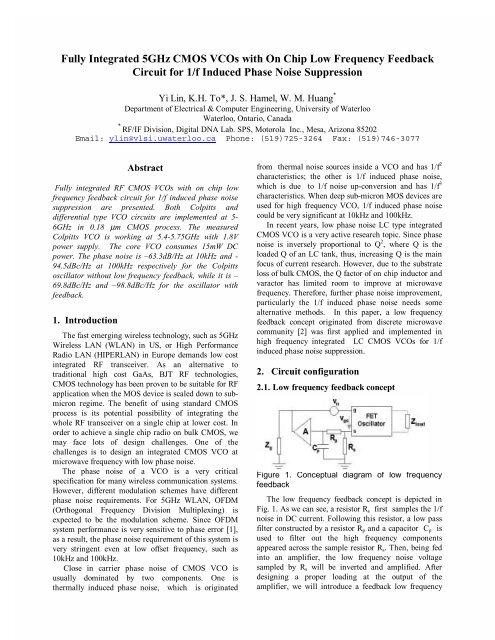
Figure 1. Conceptual diagram of low frequency<br />
feedback<br />
The low frequency feedback concept is depicted in<br />
Fig. 1. As we can see, a resistor Rs first samples the 1/f<br />
noise in DC current. Following this resistor, a low pass<br />
filter constructed by a resistor Rp and a capacitor Cp is<br />
used to filter out the high frequency components<br />
appeared across the sample resistor Rs. Then, being fed<br />
into an amplifier, the low frequency noise voltage<br />
sampled by Rs will be inverted and amplified. After<br />
designing a proper loading at the output of the<br />
amplifier, we will introduce a feedback low frequency
noise voltage in series <strong>with</strong> the equivalent 1/f noise<br />
voltage source Vn. If the feedback low frequency noise<br />
voltage has the same amplitude and 180 degree out of<br />
phase to Vn, the low frequency noise voltage across the<br />
input of active device can be canceled. Another function<br />
of the low frequency feedback is to control the DC bias<br />
of the oscillator so that the oscillator works in a more<br />
linear region, and 1/f up-conversion is reduced.<br />
2.2. <strong>CMOS</strong> VCO <strong>with</strong> low frequency feedback<br />
Figure 2 (a), (b) illustrate a Colpitts and differential<br />
<strong>CMOS</strong> VCO using a low frequency feedback. In Fig.<br />
2(a), transistor M1 and capacitor C1-C2 form a positive<br />
feedback loop to provide the negative impedance.<br />
(b)<br />
Figure 2. (a) <strong>CMOS</strong> Colpitts VCO <strong>with</strong> low<br />
frequency feedback (b) <strong>CMOS</strong> differential VCO<br />
<strong>with</strong> low frequency feedback<br />
The LC tank consists of inductor L3 and varactor C5-<br />
C6. L1 is a RF blocking inductor which will provide a<br />
high impedance at source of M1. Transistor M2 and<br />
inductor L2 are the components of a buffer amplifier.<br />
Resistor R5 is used to sample the low frequency<br />
noise. R4, C3 form a low pass filter followed by a<br />
single transistor amplifier M3. Resistor R1-R3 are parts<br />
of DC bias. In Fig. 2(b), cross coupled transistor M5,<br />
M6 provide the negative impedance to an LC tank<br />
which is constructed by inductor L3, L4 , capacitor C2,<br />
C5, and varactor C3, C4. R2 and R3 are RF blocking<br />
resistors. R10 and R11 are the sampling resistors,<br />
capacitor C9, C11, resistor R8, R9, and transistor M7,<br />
M8 form the low frequency feedback circuits. The<br />
current source bias circuit consists of transistor M1, M2<br />
(a)<br />
and resistor R1. C1, C6, C10 are the de-coupling<br />
capacitors.<br />
3. Circuit design<br />
3.1. Passive and active device RF model<br />
As shown in Fig. 2(a) (b), the integrated <strong>CMOS</strong> VCO<br />
circuits consist of many passive and active components.<br />
RF design and simulation demand accurate models of<br />
those components. For our designs, Motorola internal<br />
libraries and models were used. However, the on chip<br />
spiral inductor models were directly extracted from on<br />
wafer S-parameter measurements. As for phase noise<br />
simulation, an accurate 1/f noise model extracted from<br />
measurement [11] is also important.<br />
3.2. LC tank optimization<br />
The LC tank is the key element of LC type VCO.<br />
The oscillation frequency is determined by the product<br />
of L and C, while the oscillation amplitude and power<br />
consumption are related to the L/C ratio. Therefore,<br />
increasing L and reducing C could increase oscillation<br />
amplitude <strong>with</strong> low power consumption. However, low<br />
phase noise requires high Q LC tank which is usually<br />
determined by its inductor. For standard <strong>CMOS</strong><br />
technology, high Q large inductor at microwave<br />
frequency is usually very difficult to obtain. Thus, an<br />
optimized L/C is needed not only for high efficiency<br />
oscillation, but also for high Q inductor and varactor so<br />
as to achieve low phase noise. Moreover, proper choice<br />
of varactor value could also lead to a better tradeoff<br />
between oscillation frequency and tuning range.<br />
3.3. Phase noise consideration<br />
As an important specification, phase noise of a VCO<br />
is usually determined by linear and nonlinear<br />
mechanisms. Linear mechanism limited phase noise can<br />
be simply described by the Leeson’s model [3], which<br />
shows that the phase noise can be improved by<br />
increasing the loaded Q of the LC tank and the SNR<br />
(signal to noise ratio) of the oscillator. However,<br />
nonlinear mechanism limited phase noise is due to the<br />
inherent nonlinear properties of the oscillator. Because<br />
of these properties, the thermal noise at harmonic<br />
frequencies is down-converted to the carrier side band,<br />
while the 1/f noise source at base band is up-converted<br />
to the carrier side band. So, according to its physical<br />
source, phase noise can also be classified as thermally<br />
induced phase noise (1/f 2 slope, due to both linear and<br />
nonlinear mechanism), and 1/f induced phase noise<br />
(1/f 3 slope, only due to nonlinear mechanism). For an<br />
integrated microwave <strong>CMOS</strong> VCO, the Q improvement<br />
of on chip LC tank is limited by the lossy substrate. This<br />
will impede further phase noise improvement especially<br />
at low frequency offset, where 1/f induced phase noise is<br />
dominant because of larger 1/f noise source in deep submicron<br />
MOS devices. A carefully designed low
frequency feedback circuit described in Section 2.1 is<br />
expected to be a solution to this problem.<br />
3.4. Colpitts VCO<br />
In Fig.2 (a), the frequency of a Colpitts oscillator is<br />
determined by inductor L3, varactor C5-C6, positive<br />
feedback capacitor C1-C2 and capacitive components<br />
inside transistor M1. With positive feedback, the active<br />
device will provide a negative resistance which will<br />
compensate the loss of LC tank and start oscillation.<br />
This resistance is given by<br />
R<br />
n<br />
g<br />
= −<br />
(1)<br />
ϖ<br />
m<br />
2<br />
C 1C<br />
2<br />
For microwave oscillation, large gm and small feedback<br />
capacitor C1, C2 are usually required. Large gm requires<br />
a large transistor size which could result in large power<br />
consumption. Also, according to [4], as the phase noise<br />
of oscillator is inversely proportional to C2, increasing<br />
C2 will improve phase noise. Therefore, in order to<br />
obtain a tradeoff among oscillation frequency, power<br />
consumption, and phase noise, optimal sizing of<br />
transistor M1 and positive feedback capacitor C1 and<br />
C2 is required. Following Section 3.2, a 2nH inductor<br />
L3 and 2 parallel MOS accumulation mode varactor C5-<br />
C6 were chosen for <strong>5GHz</strong> band design. Each varactor<br />
has a tuning range from 0.65pF-1.4pF when a 2V<br />
voltage variation is applied to the varactor. All these<br />
varactors are placed in n-wells. They have the similar<br />
layout structures as MOS devices, but the doping type<br />
of their source and drain regions are same as that of nwells.<br />
The 2nH inductor is formed by a patterned<br />
electroplated copper layer. This layer is above the top<br />
layer Cu metallization and passivation. The Q of this<br />
inductor at <strong>5GHz</strong> is around 10. For transistor M1, M2<br />
and varactor C5-C6, multi-finger layout structure was<br />
adopted so as to reduce the thermal noise contribution<br />
from the gate resistance. In our design, transistor M1 is<br />
an NMOS device <strong>with</strong> 50 fingers, each finger size is<br />
2µm x 0.18µm. As an active device of the output buffer,<br />
transistor M2 will have loading effect on oscillator<br />
output. Therefore, the size of M2 will have impact on<br />
oscillation frequency, output power, and phase noise of<br />
the oscillator. Because of low 1/f noise consideration, a<br />
PMOS device is used for M2. In our design, M2 has 20<br />
fingers, each finger size is 2.5µmx0.18µm. For varactor<br />
C5-C6, each has 3 cell, each cell has 12 fingers, the<br />
finger size is 1.1µm x 9µm. In terms of low frequency<br />
feedback, the voltage gain of M3 and low pass filter<br />
bandwidth should be chosen properly. Also, low Vt<br />
MOS device for M3 is applied so that a low sampling<br />
resistor R5 can be used to ease the DC voltage drop<br />
problem.<br />
3.5. Differential VCO<br />
Although a Colpitts oscillator is widely used in<br />
wireless communication systems, a differential VCO is<br />
more suitable for integrated implementation,<br />
particularly when power supply noise and substrate<br />
noise coupling are major concerns. As shown in Fig.<br />
2(b), low frequency feedback circuits are also used in a<br />
differential VCO. Because of the space limitation, we<br />
will not describe the detail design procedure here.<br />
4. Implementation and measurement results<br />
The Colpitts and differential VCO have been<br />
implemented in a 0.18µm RF<strong>CMOS</strong> process, which is<br />
an option of a 0.18µm SiGe:C Bi<strong>CMOS</strong> technology[10].<br />
So far, only <strong>5GHz</strong> band Colpitts <strong>VCOs</strong> have been<br />
fabricated. <strong>Chip</strong> microphotographs of the Colpitts<br />
<strong>VCOs</strong> are shown in Fig. 4(a), (b). The buffer and part of<br />
the output matching circuit are integrated on chip. The<br />
size of each chip area is 1.6mm x 1.5mm. The power<br />
consumption of the Colpitts VCO <strong>with</strong> a low frequency<br />
feedback is 15mW at 1.8V voltage supply. Both wafer<br />
and board level RF testing were conducted using a HP<br />
spectrum analyzer. Fig. 5 shows the output spectrum of<br />
this VCO. By comparing <strong>with</strong> some recent <strong>CMOS</strong><br />
<strong>VCOs</strong>, we summarize the VCO performances in Table1.<br />
Table 1. Comparison of 4-<strong>5GHz</strong> <strong>CMOS</strong> <strong>VCOs</strong><br />
Tech. Freq. Tuning Phase noise Ref.<br />
(GH) Range (dBc/Hz)<br />
0.35µm<br />
<strong>CMOS</strong><br />
0.25µm<br />
<strong>CMOS</strong><br />
0.24µm<br />
SiGe<br />
Bi<strong>CMOS</strong><br />
0.18µm<br />
RF<strong>CMOS</strong><br />
4.7 4.3% -62 @10kHz<br />
-90 @100kHz<br />
5.05 18% -62.5@10kHz<br />
-94 @100kHz<br />
5.67 14.9% -63 @10kHz<br />
-96 @100kHz<br />
5.74 6.1% -69 @10kHz<br />
-98 @100kHz<br />
(6)<br />
(8)<br />
(9)<br />
This<br />
work<br />
(a) (b)<br />
Figure 4. Microphotograph of the <strong>CMOS</strong> Colpitts<br />
VCO (a) <strong>with</strong>out low frequency feedback (b) <strong>with</strong><br />
low frequency feedback<br />
With regards to the phase noise, first, an HB<br />
(Harmonic Balance) phase noise simulator is used to<br />
simulate the effectiveness of this low frequency feedback<br />
phase noise reduction technique. Then, it is verified by
the measurement data. Fig. 6 shows the simulation and<br />
measurement results of the Colpitts <strong>VCOs</strong> <strong>with</strong> and<br />
<strong>with</strong>out feedback. As we can see, the feedback method<br />
results in a noticeable phase noise reduction(4-6dB) at<br />
low offset frequency(10kHz-100kHz) where 1/f upconversion<br />
is significant.<br />
Figure 5. Output spectrum of the <strong>5GHz</strong> band <strong>CMOS</strong><br />
Colpitts VCO <strong>with</strong> low frequency feedback<br />
Phase Noise(dBc/Hz)<br />
Phase Noise(dBc/Hz)<br />
-60<br />
-80<br />
-100<br />
-120<br />
-60<br />
-80<br />
-100<br />
-120<br />
10 4<br />
10 4<br />
(b)<br />
Figure 6. Phase noise results of <strong>CMOS</strong> Colpitts<br />
<strong>VCOs</strong> at 5.74GHz (a) simulation (b) measurement<br />
5. Conclusions<br />
10 5<br />
Offset <strong>Frequency</strong> (Hz)<br />
(a)<br />
With Feedback<br />
No Feedback<br />
With Feedback<br />
No Feedback<br />
10 5<br />
Offset <strong>Frequency</strong> (Hz)<br />
Compared <strong>with</strong> other wireless systems, a OFDM<br />
WLAN system has more stringent phase noise<br />
requirements for its local oscillator [1]. In particular,<br />
the phase noise specs at low offset frequencies, where<br />
1/f induced phase noise could be dominant, are expected<br />
to be the bottlenecks for integrated <strong>5GHz</strong> LC VCO<br />
implementation using deep sub-micron bulk <strong>CMOS</strong><br />
technology. The Q improvement of LC tank in bulk<br />
<strong>CMOS</strong> has a physical limit, this limit will make further<br />
phase noise reduction, especially the 1/f induced phase<br />
noise reduction very difficult. In this paper, an<br />
10 6<br />
10 6<br />
alternative low frequency feedback technique was<br />
applied to reduce the 1/f induced phase noise in fully<br />
integrated <strong>5GHz</strong> <strong>CMOS</strong> <strong>VCOs</strong>. The simulation results<br />
and measurement data of two different Colpitts <strong>VCOs</strong><br />
have proved the effectiveness of this technique for phase<br />
noise reduction at offset frequency smaller than 200kHz.<br />
The advantage of this technique is its simple, low cost,<br />
and compatibility <strong>with</strong> any other phase noise reduction<br />
techniques. This technique can also be applied for<br />
<strong>VCOs</strong> fabricated in different technologies and will not<br />
be limited by operating frequency and technology<br />
scaling.<br />
6. Acknowledgements<br />
The authors wish to greatly acknowledge Motorola<br />
Inc. for CAD support and VCO fabrication. They also<br />
wish to thank Joe Street in SiDiC Group of University<br />
of Waterloo for his technical assistance in chip bonding.<br />
7. References<br />
[1] J. R. Pelliccio, H. Bachmann, B. W. Myers, “Phase Noise<br />
Effect on OFDM Wireless LAN Performance,” Applied<br />
Microwave & Wireless, vol. 13, no. 7, pp. 68-78, 2001.<br />
[2] M. Prigent, J. Obregon, “ Phase Noise Reduction in FET<br />
Oscillators by <strong>Low</strong> <strong>Frequency</strong> Loading and Feedback<br />
Circuitry Optimization,” IEEE Trans. Microwave Theory<br />
Tech., vol. MTT-35, no. 3, pp. 349-352, March 1987.<br />
[3] D. B. Leeson, “ A simple model of feedback oscillator<br />
noise spectrum,” Proc. IEEE, vol.54, pp.329-330, Feb.<br />
1966.<br />
[4] Ulrich L. Rohde, Frank Hagemeyer, “Feedback<br />
Technique Improves Oscillator Phase Noise,” Microwave<br />
& RF, vol. MTT-35, no. 3, pp. 61-70, May 1998.<br />
[5] XiangDong Zhang, James Kramer, Brian Rizzi, “A<br />
Theoretical and Experimental Study on <strong>Low</strong>-voltage Bias<br />
Voltage Controlled Oscillators,” 1997 IEEE MTT-S<br />
Digest, pp. 845-848, 1997.<br />
[6] P. Kinget, “ A <strong>Fully</strong> integrated 2.7V 0.35um <strong>CMOS</strong><br />
VCO for <strong>5GHz</strong> wireless Applications,” IEEE ISSCC Dig.<br />
Tech. Papers, pp. 226-227, Feb. 1998.<br />
[7] M. Soyuer, K. A. Jenkins, J. N. Burghartz, “ A 3V 4GHz<br />
nMOS Voltage-Controlled Oscillator <strong>with</strong> <strong>Integrated</strong><br />
Resonator, ” IEEE ISSCC Dig. Tech. Papers, pp. 394-<br />
395, Feb. 1996.<br />
[8] C. Samori, S. Levantino, V. Boccuzzi, “ A –<br />
94dBc/Hz@100kHz, fully-integrated, 5-GHz, <strong>CMOS</strong><br />
VCO <strong>with</strong> 18% tuning range for Bluetooth applications,”<br />
Proc. IEEE CICC, pp. 201-204, May 2001.<br />
[9] H. Ainspan, J. O. Plouchart, “ A Comparison of MOS<br />
Varactors in <strong>Fully</strong>-<strong>Integrated</strong> <strong>CMOS</strong> LC VCO’s at 5 and<br />
7GHz,” Proc. ESSCIRC, pp. 448-451, 2000.<br />
[10] J. Kirchgessner, et al., “A 0.18µm SiGe:C RF Bi<strong>CMOS</strong><br />
Technology for Wireless and Gigabit Optical<br />
Communication Applications,” Proc. IEEE BCTM , pp.<br />
151-154, 2001.<br />
[11] A. Blaum, O. Pilloud, G. Scalea, J. Victory, F. Sischka,<br />
“ A New Robust <strong>On</strong>-Wafer 1/f Noise Measurement and<br />
Characterization System,” Proc. IEEE 2001 Int.<br />
Conference on Microelectronic Test Structures, pp. 125-<br />
130, March 2001.


