
You also want an ePaper? Increase the reach of your titles
YUMPU automatically turns print PDFs into web optimized ePapers that Google loves.
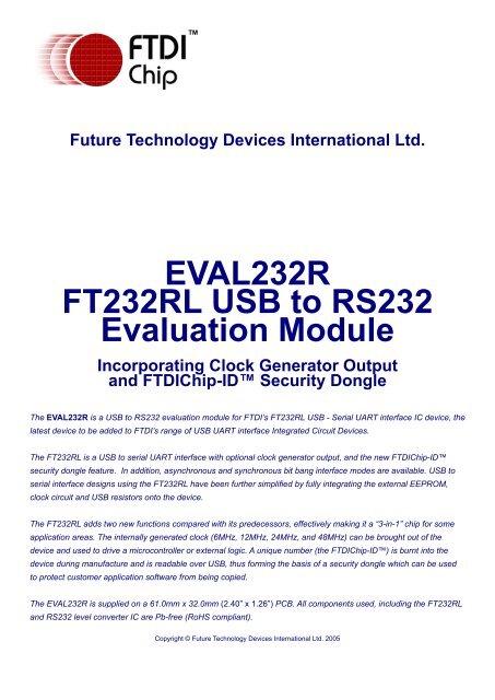
Future Technology Devices International Ltd.<br />
<strong>EVAL232R</strong><br />
FT232RL USB to RS232<br />
Evaluation Module<br />
Incorporating Clock Generator Output<br />
and <strong>FTDI</strong>Chip-ID Security Dongle<br />
The <strong>EVAL232R</strong> is a USB to RS232 evaluation module for <strong>FTDI</strong>’s FT232RL USB - Serial UART interface IC device, the<br />
latest device to be added to <strong>FTDI</strong>’s range of USB UART interface Integrated Circuit Devices.<br />
The FT232RL is a USB to serial UART interface with optional clock generator output, and the new <strong>FTDI</strong>Chip-ID<br />
security dongle feature. In addition, asynchronous and synchronous bit bang interface modes are available. USB to<br />
serial interface designs using the FT232RL have been further simplified by fully integrating the external EEPROM,<br />
clock circuit and USB resistors onto the device.<br />
The FT232RL adds two new functions compared with its predecessors, effectively making it a “3-in-1” chip for some<br />
application areas. The internally generated clock (6MHz, 12MHz, 24MHz, and 48MHz) can be brought out of the<br />
device and used to drive a microcontroller or external logic. A unique number (the <strong>FTDI</strong>Chip-ID) is burnt into the<br />
device during manufacture and is readable over USB, thus forming the basis of a security dongle which can be used<br />
to protect customer application software from being copied.<br />
The <strong>EVAL232R</strong> is supplied on a 61.0mm x 32.0mm (2.40” x 1.26”) PCB. All components used, including the FT232RL<br />
and RS232 level converter IC are Pb-free (RoHS compliant).<br />
Copyright © Future Technology Devices International Ltd. 2005
1. Features<br />
1.1 Hardware Features<br />
• FT232RL provides single chip USB to<br />
asynchronous serial data transfer interface.<br />
• Module provides USB to RS232 interface, with<br />
additional I/O pinout.<br />
• Entire USB protocol handled on the FT232RL chip<br />
- No USB-specific firmware programming required.<br />
• UART interface support for 7 or 8 data bits, 1 or 2<br />
stop bits and odd / even / mark / space / no parity.<br />
• Fully assisted hardware or X-On / X-Off software<br />
handshaking.<br />
• Data transfer rates from 300 baud to 1 Megabaud<br />
at RS232 levels.<br />
• <strong>FTDI</strong>’s royalty-free VCP and D2XX drivers<br />
eliminate the requirement for USB driver<br />
development in most cases.<br />
• In-built support for event characters and line break<br />
condition.<br />
• New USB <strong>FTDI</strong>Chip-ID feature.<br />
• New configurable CBUS I/O pins.<br />
• Transmit and receive LED’s to indicate serial data<br />
transfer.<br />
• New 48MHz, 24MHz,12MHz, and 6MHz clock<br />
output signal Options.<br />
• FIFO receive and transmit buffers for high data<br />
throughput.<br />
• Adjustable receive buffer timeout.<br />
• Synchronous and asynchronous bit bang mode<br />
interface options with RD# and WR# strobes.<br />
• New CBUS bit bang mode option.<br />
• Integrated 1024 bit internal EEPROM for storing<br />
USB VID, PID, serial number and product<br />
description strings, and CBUS I/O configuration.<br />
1.2 Driver Support<br />
Royalty-Free VIRTUAL COM PORT<br />
(VCP) DRIVERS for...<br />
• Windows 98, 98SE, ME, 2000, Server 2003, XP.<br />
• Windows Vista / Longhorn*<br />
• Windows XP 64-bit.*<br />
• Windows XP Embedded.<br />
• Windows CE.NET 4.2 & 5.0<br />
• MAC OS 8 / 9, OS-X<br />
• Linux 2.4 and greater<br />
<strong>EVAL232R</strong> FT232RL USB to RS232 Evaluation Module <strong>Datasheet</strong> Version 0.90 © Future Technology Devices International Ltd. 2005<br />
Page 2<br />
• Device supplied preprogrammed with unique USB<br />
serial number.<br />
• Support for USB suspend and resume.<br />
• Module supply voltage comes from VCC - no<br />
external supply required.<br />
• 5V USB power available to supply external<br />
devices.<br />
• Integrated 3.3V level converter for USB I/O .<br />
• Integrated level converter on UART and CBUS for<br />
interfacing to 5V - 1.8V Logic.<br />
• On board jumper allows for selection of UART and<br />
CBUS interface IO voltage.<br />
• True 5V / 3.3V / 2.8V / 1.8V CMOS drive output<br />
and TTL input.<br />
• High I/O pin output drive option.<br />
• Integrated USB resistors.<br />
• Integrated power-on-reset circuit.<br />
• Fully integrated clock - no external crystal,<br />
oscillator, or resonator required.<br />
• Fully integrated AVCC supply filtering - No separate<br />
AVCC pin and no external R-C filter required.<br />
• USB bulk transfer mode.<br />
• Low operating and USB suspend current.<br />
• Low USB bandwidth consumption.<br />
• UHCI / OHCI / EHCI host controller compatible<br />
• USB 2.0 Full Speed compatible.<br />
• -40°C to 85°C extended operating temperature<br />
range.<br />
• Supplied on minature 61.0mm x 32.0mm (2.40” x<br />
1.26”) PCB with 15 board header pins.<br />
• Connect to a PC via a standard USB A to B USB<br />
cable.<br />
Royalty-Free D2XX Direct Drivers<br />
(USB Drivers + DLL S/W Interface)<br />
• Windows 98, 98SE, ME, 2000, Server 2003, XP.<br />
• Windows Vista / Longhorn*<br />
• Windows XP 64-bit.*<br />
• Windows XP Embedded.<br />
• Windows CE.NET 4.2 & 5.0<br />
• Linux 2.4 and greater<br />
The drivers listed above are all available to download for free from the <strong>FTDI</strong> website. Various 3rd Party Drivers are<br />
also available for various other operating systems - see the <strong>FTDI</strong> website for details.<br />
* Currently Under Development. Contact <strong>FTDI</strong> for availability.<br />
1.3 Typical Applications<br />
• USB to RS232 Converter<br />
• Upgrading Legacy Peripherals to USB<br />
• USB Audio and Low Bandwidth Video data transfer<br />
• PDA to USB data transfer<br />
• USB Smart Card Readers<br />
• USB Instrumentation<br />
• USB Industrial Control<br />
• USB MP3 Player Interface<br />
• USB FLASH Card Reader / Writers<br />
• Set Top Box PC - USB interface<br />
• USB Digital Camera Interface<br />
• USB Hardware Modems<br />
• USB Wireless Modems<br />
• USB Bar Code Readers<br />
• USB Software / Hardware Encryption Dongles
2. Features and Enhancements<br />
2.1 Key Features<br />
This section summarises the key features and enhancements of the FT232RL IC device which is used on the<br />
<strong>EVAL232R</strong> Module. For further details, consult the FT232R datasheet, which is available from the <strong>FTDI</strong> website.<br />
Integrated Clock Circuit - Previous generations of <strong>FTDI</strong>’s USB UART devices required an external crystal or ceramic<br />
resonator. The clock circuit has now been integrated onto the device meaning that no crystal or ceramic resonator is<br />
required. However, if required, an external 12MHz crystal can be used as the clock source.<br />
Integrated EEPROM - Previous generations of <strong>FTDI</strong>’s USB UART devices required an external EEPROM if the<br />
device were to use USB Vendor ID (VID), Product ID (PID), serial number and product description strings other than<br />
the default values in the device itself. This external EEPROM has now been integrated onto the FT232R chip meaning<br />
that all designs have the option to change the product description strings. A user area of the internal EEPROM is<br />
available for storing additional data. The internal EEPROM is programmable in circuit, over USB without any additional<br />
voltage requirement.<br />
Preprogrammed EEPROM - The FT232R is supplied with its internal EEPROM preprogrammed with a serial number<br />
which is unique to each individual device. This, in most cases, will remove the need to program the device EEPROM.<br />
Integrated USB Resistors - Previous generations of <strong>FTDI</strong>’s USB UART devices required two external series resistors<br />
on the USBDP and USBDM lines, and a 1.5 kΩ pull up resistor on USBDP. These three resistors have now been<br />
integrated onto the device.<br />
Integrated AVCC Filtering - Previous generations of <strong>FTDI</strong>’s USB UART devices had a separate AVCC pin - the<br />
supply to the internal PLL. This pin required an external R-C filter. The separate AVCC pin is now connected internally<br />
to VCC, and the filter has now been integrated onto the chip.<br />
Less External Components - Integration of the crystal, EEPROM, USB resistors, and AVCC filter will substantially<br />
reduce the bill of materials cost for USB interface designs using the FT232R compared to its FT232BM predecessor.<br />
Configurable CBUS I/O Pin Options - There are now 5 configurable Control Bus (CBUS) lines. Options are TXDEN<br />
- transmit enable for RS485 designs, PWREN# - Power control for high power, bus powered designs, TXLED# - for<br />
pulsing an LED upon transmission of data, RXLED# - for pulsing an LED upon receiving data, TX&RXLED# - which<br />
will pulse an LED upon transmission OR reception of data, SLEEP# - indicates that the device going into USB<br />
suspend mode, CLK48 / CLK24 / CLK12 / CLK6 - 48MHz, 24MHz,12MHz, and 6MHz clock output signal options.<br />
There is also the option to bring out bit bang mode read and write strobes (see below). The CBUS lines can be<br />
configured with any one of these output options by setting bits in the internal EEPROM. The device is supplied with<br />
the most commonly used pin definitions preprogrammed - see Section 8 for details.<br />
Enhanced Asynchronous Bit Bang Mode with RD# and WR# Strobes - The FT232R supports <strong>FTDI</strong>’s BM chip<br />
bit bang mode. In bit bang mode, the eight UART lines can be switched from the regular interface mode to an 8-bit<br />
general purpose I/O port. Data packets can be sent to the device and they will be sequentially sent to the interface<br />
at a rate controlled by an internal timer (equivalent to the baud rate prescaler). With the FT232R device this mode<br />
has been enhanced so that the internal RD# and WR# strobes are now brought out of the device which can be used<br />
to allow external logic to be clocked by accesses to the bit bang I/O bus. This option will be described more fully in a<br />
separate application note.<br />
Synchronous Bit Bang Mode - Synchronous bit bang mode differs from asynchronous bit bang mode in that the<br />
interface pins are only read when the device is written to. Thus making it easier for the controlling program to measure<br />
the response to an output stimulus as the data returned is synchronous to the output data. The feature was previously<br />
seen in <strong>FTDI</strong>’s FT2232C device. This option will be described more fully in a separate application note.<br />
CBUS Bit Bang Mode - This mode allows four of the CBUS pins to be individually configured as GPIO pins, similar<br />
to Asynchronous bit bang mode. It is possible to use this mode while the UART interface is being used, thus providing<br />
up to four general purpose I/O pins which are available during normal operation. An application note describing this<br />
feature is available separately from the <strong>FTDI</strong> website.<br />
<strong>EVAL232R</strong> FT232RL USB to RS232 Evaluation Module <strong>Datasheet</strong> Version 0.90 © Future Technology Devices International Ltd. 2005<br />
Page 3
Page 4<br />
Lower Supply Voltage - Previous generations of the chip required 5V supply on the VCC pin. The FT232R will work<br />
with a Vcc supply in the range 3.3V - 5.25V. Bus powered designs would still take their supply from the 5V on the USB<br />
bus, but for self powered designs where only 3.3V is available and there is no 5V supply there is no longer any need<br />
for an additional external regulator.<br />
Integrated Level Converter on UART Interface and Control Signals - VCCIO pin supply can be from 1.8V to 5V.<br />
Connecting the VCCIO pin to 1.8V, 2.8V, or 3.3V allows the device to directly interface to 1.8V, 2.8V or 3.3V and other<br />
logic families without the need for external level converter I.C. devices.<br />
5V / 3.3V / 2.8V / 1.8V Logic Interface - The FT232R provides true CMOS Drive Outputs and TTL level Inputs.<br />
Integrated Power-On-Reset (POR) Circuit- The device incorporates an internal POR function. A RESET# pin is<br />
available in order to allow external logic to reset the FT232R where required. However, for many applications the<br />
RESET# pin can be left unconnected, or pulled up to VCCIO.<br />
Lower Operating and Suspend Current - The device operating supply current has been further reduced to 15mA,<br />
and the suspend current has been reduced to around 70μA. This allows greater margin for peripheral designs to meet<br />
the USB suspend current limit of 500μA.<br />
Low USB Bandwidth Consumption - The operation of the USB interface to the FT232R has been designed to use<br />
as little as possible of the total USB bandwidth available from the USB host controller.<br />
High Output Drive Option - The UART interface and CBUS I/O pins can be made to drive out at three times the<br />
standard signal drive level thus allowing multiple devices to be driven, or devices that require a greater signal drive<br />
strength to be interfaced to the FT232R. This option is enabled in the internal EEPROM.<br />
Power Management Control for USB Bus Powered, High Current Designs- The PWREN# signal can be used to<br />
directly drive a transistor or P-Channel MOSFET in applications where power switching of external circuitry is required.<br />
An option in the internal EEPROM makes the device gently pull down on its UART interface lines when the power<br />
is shut off (PWREN# is high). In this mode any residual voltage on external circuitry is bled to GND when power is<br />
removed, thus ensuring that external circuitry controlled by PWREN# resets reliably when power is restored.<br />
UART Pin Signal Inversion - The sense of each of the eight UART signals can be individually inverted by setting<br />
options in the internal EEPROM. Thus, CTS# (active low) can be changed to CTS (active high), or TXD can be<br />
changed to TXD#.<br />
<strong>FTDI</strong>Chip-ID - Each FT232R is assigned a unique number which is burnt into the device at manufacture. This ID<br />
number cannot be reprogrammed by product manufacturers or end-users. This allows the possibility of using FT232R<br />
based dongles for software licensing. Further to this, a renewable license scheme can be implemented based on the<br />
<strong>FTDI</strong>Chip-ID number when encrypted with other information. This encrypted number can be stored in the user area<br />
of the FT232R internal EEPROM, and can be decrypted, then compared with the protected <strong>FTDI</strong>Chip-ID to verify<br />
that a license is valid. Web based applications can be used to maintain product licensing this way. An application note<br />
describing this feature is available separately from the <strong>FTDI</strong> website.<br />
Improved EMI Performance - The reduced operating current and improved on-chip VCC decoupling significantly<br />
improves the ease of PCB design requirements in order to meet FCC, CE and other EMI related specifications.<br />
Programmable Receive Buffer Timeout - The receive buffer timeout is used to flush remaining data from the<br />
receive buffer. This time defaults to 16ms, but is programmable over USB in 1ms increments from 1ms to 255ms, thus<br />
allowing the device to be optimised for protocols that require fast response times from short data packets.<br />
Baud Rates - The FT232R supports all standard baud rates and non-standard baud rates from 300 Baud up to 3<br />
Megabaud. Achievable non-standard baud rates are calculated as follows -<br />
Baud Rate = 3000000 / (n + x)<br />
where n can be any integer between 2 and 16,384 ( = 2 14 ) and x can be a sub-integer of the value 0, 0.125, 0.25,<br />
0.375, 0.5, 0.625, 0.75, or 0.875. When n = 1, x = 0, i.e. baud rate divisors with values between 1 and 2 are not<br />
possible.<br />
This gives achievable baud rates in the range 183.1 baud to 3,000,000 baud. When a non-standard baud rate is<br />
required simply pass the required baud rate value to the driver as normal, and the <strong>FTDI</strong> driver will calculate the<br />
required divisor, and set the baud rate. See <strong>FTDI</strong> application note AN232B-05 for more details.<br />
<strong>EVAL232R</strong> FT232RL USB to RS232 Evaluation Module <strong>Datasheet</strong> Version 0.90 © Future Technology Devices International Ltd. 2005
Extended Operating Temperature Range - The FT232R operates over an extended temperature range of -40º to<br />
+85º C thus allowing the device to be used in automotive and industrial applications.<br />
New Package Options - The FT232R is available in two packages - a compact 28 pin SSOP ( FT232RL) and an<br />
ultra-compact 5mm x 5mm pinless QFN-32 package ( FT232RQ). Both packages are lead ( Pb ) free, and use a<br />
‘green’ compound. Both packages are fully compliant with European Union directive 2002/95/EC. The MM232R<br />
module uses a FT232RQ device in its design.<br />
Figure 1 - The <strong>EVAL232R</strong> Development Module.<br />
<strong>EVAL232R</strong> FT232RL USB to RS232 Evaluation Module <strong>Datasheet</strong> Version 0.90 © Future Technology Devices International Ltd. 2005<br />
Page 5
3. <strong>EVAL232R</strong> Pin Out and Signal Descriptions<br />
3.1 <strong>EVAL232R</strong> Pin Out<br />
LP1<br />
LP2<br />
TX<br />
LED<br />
RX<br />
LED<br />
Figure 2 - <strong>EVAL232R</strong> Module Pin Out.<br />
1 2<br />
3 4<br />
Figure 3 - <strong>EVAL232R</strong> RS232 (DB9) Pin Out<br />
J3<br />
GND<br />
RESET#<br />
VCCIO<br />
CBUS3<br />
CBUS2<br />
CBUS1<br />
CBUS0<br />
VCC<br />
<strong>FTDI</strong><br />
VCC30<br />
VCCIO<br />
VCC<br />
<strong>EVAL232R</strong> FT232RL USB to RS232 Evaluation Module <strong>Datasheet</strong> Version 0.90 © Future Technology Devices International Ltd. 2005<br />
J1<br />
DCD RXD TXD<br />
1<br />
DSR<br />
6<br />
1 2 3 4 5 6 7 8<br />
1 2 3<br />
2<br />
DTR<br />
J2<br />
3 4 5<br />
RTS CTS<br />
RI<br />
7 8 9<br />
GND<br />
Page 6
3.2 Header Pin and Jumper Signal Descriptions<br />
Table 1 - Module Pin Out Description - Jumper J1<br />
Pin No. Name Type Description<br />
1 VCC Output 5V Power output USB port. For a low power USB bus powered design, up to 100mA can be sourced from the<br />
5V supply on the USB bus. A maximum of 500mA can be sourced from the USB bus in a high power USB bus<br />
powered design.<br />
2 VCCIO Input +1.8V to +5.25V supply to the FT232RL’s UART Interface and CBUS I/O pins. In USB bus powered designs<br />
connect to 3V3 to drive out at 3.3V levels (connect VCCIO to VCC3O), or connect to VCC to drive out at 5V<br />
CMOS level (connect VCCIO to VCC). This pin can also be supplied with an external 1.8V - 2.8V supply in<br />
order to drive out at lower levels. It should be noted that in this case this supply should originate from the<br />
same source as the supply to Vcc. This means that in bus powered designs (like the <strong>EVAL232R</strong> for example)<br />
a regulator which is supplied by the 5V on the USB bus should be used.<br />
3 VCC3O Output 3.3V output from FT232RL’s integrated L.D.O. regulator. This pin is decoupled to ground on the module pcb<br />
with a 100nF capacitor. The prime purpose of this pin is to provide the internal 3.3V supply to the USB transceiver<br />
cell and the internal 1.5kΩ pull up resistor on USBDP. Up to 50mA can be drawn from this pin to power<br />
external logic if required. This pin can also be used to supply the FT232RL’s VCCIO pin by connecting this pin<br />
to pin 3 (VCCIO).<br />
Table 2 - Module Pin Out Description - 8 Pin Header J2<br />
Pin No. Name Type Description<br />
1 VCC Output 5V Power output USB port. For a low power USB bus powered design, up to 100mA can be sourced from the<br />
5V supply on the USB bus. A maximum of 500mA can be sourced from the USB bus in a high power USB bus<br />
powered design.<br />
2 CBUS0 Input Configurable CBUS I/O Pin. Function of this pin is configured in the device internal EEPROM. Factory default<br />
pin function for the <strong>EVAL232R</strong> module is RXLED#. See CBUS Signal Options, Table 4.*<br />
3 CBUS1 Output Configurable CBUS I/O Pin. Function of this pin is configured in the device internal EEPROM. Factory default<br />
pin function for the <strong>EVAL232R</strong> module is TXLED#. See CBUS Signal Options, Table 4.*<br />
4 CBUS2 Output Configurable CBUS I/O Pin. Function of this pin is configured in the device internal EEPROM. Factory default<br />
pin function for the <strong>EVAL232R</strong> module is PWREN#. See CBUS Signal Options, Table 4.*<br />
5 CBUS3 Output Configurable CBUS I/O Pin. Function of this pin is configured in the device internal EEPROM. Factory default<br />
pin function for the <strong>EVAL232R</strong> module is PWREN#. See CBUS Signal Options, Table 4.*<br />
6 VCC3O Output 3.3V output from FT232RL’s integrated L.D.O. regulator. This pin is decoupled to ground on the module pcb<br />
with a 100nF capacitor. The prime purpose of this pin is to provide the internal 3.3V supply to the USB transceiver<br />
cell and the internal 1.5kΩ pull up resistor on USBDP. Up to 50mA can be drawn from this pin to power<br />
external logic if required.<br />
7 RESET# Input Can be used by an external device to reset the FT232R. If not required can be left unconnected, or pulled up<br />
to VCCIO.<br />
3 GND GND Module ground supply pins<br />
Table 3 - Module Pin Out Description - Jumper J3<br />
Pin No. Name Type Description<br />
1 CBUS0 Output Configurable CBUS I/O Pin. Function of this pin is configured in the device internal EEPROM. Factory default<br />
pin function for the <strong>EVAL232R</strong> module is RXLED#. See CBUS Signal Options, Table 4.*<br />
Connect to LP1 to drive the red receive data LED (module default)<br />
2 LP1 Input Red receive data LED<br />
3 CBUS1 Output Configurable CBUS I/O Pin. Function of this pin is configured in the device internal EEPROM. Factory default<br />
pin function for the <strong>EVAL232R</strong> module is TXLED#. See CBUS Signal Options, Table 4.*<br />
Connect to LP2 to drive the green transmit data LED (module default)<br />
3 LP2 Intput Green transmit data LED<br />
* When used in Input Mode, these pins are pulled to VCCIO via internal 200kΩ resistors. These pins can be<br />
programmed to gently pull low during USB suspend ( PWREN# = “1” ) by setting an option in the internal EEPROM.<br />
<strong>EVAL232R</strong> FT232RL USB to RS232 Evaluation Module <strong>Datasheet</strong> Version 0.90 © Future Technology Devices International Ltd. 2005<br />
Page 7
3.3 CBUS Signal Options<br />
The following options can be configured on the CBUS I/O pins. These options are all configured in the internal<br />
EEPROM using the utility software MPROG, which can be downloaded from the <strong>FTDI</strong> website. The default<br />
configuration is described in Section 8.<br />
Table 4 - CBUS Signal Options<br />
CBUS Signal Option Available On CBUS Pin... Description<br />
TXDEN CBUS0, CBUS1, CBUS2, CBUS3, CBUS4 Enable transmit data for RS485<br />
TXLED# CBUS0, CBUS1, CBUS2, CBUS3, CBUS4 Transmit data LED drive - pulses low when transmitting data via<br />
USB. See FT232R datasheet for more details.<br />
RXLED# CBUS0, CBUS1, CBUS2, CBUS3, CBUS4 Receive data LED drive - pulses low when receiving data via USB.<br />
See FT232R datasheet for more details.<br />
TX&RXLED# CBUS0, CBUS1, CBUS2, CBUS3, CBUS4 LED drive - pulses low when transmitting or receiving data via<br />
USB. See FT232R datasheet for more details.<br />
PWREN# CBUS0, CBUS1, CBUS2, CBUS3, CBUS4 Goes low after the device is configured by USB, then high during<br />
USB suspend. Can be used to control power to external logic P-<br />
Channel logic level MOSFET switch. Enable the interface pull-down<br />
option when using the PWREN# pin in this way.<br />
SLEEP# CBUS0, CBUS1, CBUS2, CBUS3, CBUS4 Goes low during USB suspend mode. Typically used to power down<br />
an external TTL to RS232 level converter I.C. in USB to RS232<br />
converter designs.<br />
CLK48 CBUS0, CBUS1, CBUS2, CBUS3, CBUS4 48MHz Clock output.<br />
CLK24 CBUS0, CBUS1, CBUS2, CBUS3, CBUS4 24MHz Clock output.<br />
CLK12 CBUS0, CBUS1, CBUS2, CBUS3, CBUS4 12MHz Clock output.<br />
CLK6 CBUS0, CBUS1, CBUS2, CBUS3, CBUS4 6MHz Clock output.<br />
CBitBangI/O CBUS0, CBUS1, CBUS2, CBUS3 CBUS bit bang mode option. Allows up to 4 of the CBUS pins to be<br />
used as general purpose I/O. Configured individually for CBUS0,<br />
CBUS1, CBUS2 and CBUS3 in the internal EEPROM. A separate<br />
application note will describe in more detail how to use CBUS bit<br />
bang mode.<br />
BitBangWRn CBUS0, CBUS1, CBUS2, CBUS3 Synchronous and asynchronous bit bang mode WR# strobe Output<br />
BitBangRDn CBUS0, CBUS1, CBUS2, CBUS3 Synchronous and asynchronous bit bang mode RD# strobe Output<br />
3.4 RS232 Signal Descriptions<br />
Table 5 - RS232 Signals<br />
DB9 pin No. Name Type Description<br />
1 DCD Input Data Carrier Detect control input<br />
2 RXDATA Input Receive Asynchronous Data input.<br />
3 TXDATA Output Transmit Asynchronous Data output.<br />
4 DTR Output Data Terminal Ready control output / Handshake signal<br />
5 GND GND Device groud supply pin.<br />
6 DSR Input Data Set Ready control input / Handshake signal<br />
7 RTS Output Request To Send Control Output / Handshake signal.<br />
8 CTS Input Clear to Send Control input / Handshake signal.<br />
9 RI Input Ring Indicator control input. When remote wakeup is enabled in the FT232RL’s internal<br />
EEPROM taking RI# low can be used to resume the PC USB host controller from suspend.<br />
<strong>EVAL232R</strong> FT232RL USB to RS232 Evaluation Module <strong>Datasheet</strong> Version 0.90 © Future Technology Devices International Ltd. 2005<br />
Page 8
4. Module Dimensions<br />
3.25mm (0.13")<br />
12.00mm<br />
(0.48")<br />
12.5mm<br />
(0.50")<br />
2.75mm<br />
(0.11")<br />
LP1<br />
LP2<br />
Figure 4 - <strong>EVAL232R</strong> Module Dimensions<br />
All dimensions are stated in millimeters, with inches in parenthesis.<br />
The FT232RL is supplied in a RoHS compliant 28 pinSSOP package. The package is lead ( Pb ) free and uses a<br />
‘green’ compound. The date code format is YYXX where XX = 2 digit week number, YY = 2 digit year number.<br />
The <strong>EVAL232R</strong> module uses exclusivly lead free components.<br />
J3<br />
Ø 2.50mm<br />
(0.10")<br />
2.55mm<br />
(0.10")<br />
4.95mm<br />
(0.20")<br />
<strong>FTDI</strong><br />
61.50mm<br />
(2.46")<br />
3.25mm<br />
(0.13")<br />
12.50mm<br />
(0.50")<br />
7.00mm<br />
(0.28")<br />
5.50mm<br />
(0.22")<br />
Both the I.C. device and the module are fully compliant with European Union directive 2002/95/EC.<br />
J1<br />
0.65mm<br />
(0.03")<br />
20.00mm<br />
(0.80")<br />
61.00mm<br />
(2.44")<br />
18.00mm<br />
(0.72")<br />
<strong>EVAL232R</strong> FT232RL USB to RS232 Evaluation Module <strong>Datasheet</strong> Version 0.90 © Future Technology Devices International Ltd. 2005<br />
J2<br />
1.90mm<br />
(0.08")<br />
11.80mm<br />
(0.47")<br />
4.70mm (0.19")<br />
9.30mm<br />
(0.37")<br />
1.60mm (0.06")<br />
Page 9<br />
32.00mm<br />
(1.28")<br />
14.35mm<br />
(0.57")
5. Device Characteristics and Ratings<br />
5.1 Absolute Maximum Ratings<br />
The absolute maximum ratings for the FT232R devices are as follows. These are in accordance with the Absolute<br />
Maximum Rating System (IEC 60134). Exceeding these may cause permanent damage to the device.<br />
Table 6 - Absolute Maximum Ratings<br />
Parameter Value Unit<br />
Storage Temperature -65°C to 150°C Degrees C<br />
Floor Life (Out of Bag) At Factory Ambient<br />
( 30°C / 60% Relative Humidity)<br />
168 Hours<br />
(IPC/JEDEC J-STD-033A MSL<br />
Level 3 Compliant)*<br />
Ambient Temperature (Power Applied) -40°C to 85°C Degrees C.<br />
Vcc Supply Voltage -0.5 to +6.00 V<br />
D.C. Input Voltage - USBDP and USBDM -0.5 to +3.8 V<br />
D.C. Input Voltage - High Impedance Bidirectionals -0.5 to +(Vcc +0.5) V<br />
D.C. Input Voltage - All other Inputs -0.5 to +(Vcc +0.5) V<br />
D.C. Output Current - Outputs 24 mA<br />
DC Output Current - Low Impedance Bidirectionals 24 mA<br />
Power Dissipation (Vcc = 5.25V) 500 mW<br />
* If devices are stored out of the packaging beyond this time limit the devices should be baked before use. The<br />
devices should be ramped up to a temperature of 125°C and baked for up to 17 hours.<br />
5.2 DC Characteristics<br />
DC Characteristics ( Ambient Temperature = -40 to 85 o C )<br />
Table 7 - Operating Voltage and Current<br />
Parameter Description Min Typ Max Units Conditions<br />
Vcc1 VCC Operating Supply Voltage 3.3 - 5.25 V<br />
Vcc2 VCCIO Operating Supply Voltage 1.8 - 5.25 V<br />
Icc1 Operating Supply Current - 15 - mA Normal Operation<br />
Icc2 Operating Supply Current 50 70 100 μA USB Suspend*<br />
Table 8 - FT232R UART and CBUS I/O Pin Characteristics (VCCIO = 5.0V, Standard Drive Level)<br />
Parameter Description Min Typ Max Units Conditions<br />
Voh Output Voltage High 3.2 4.1 4.9 V I source = 2mA<br />
Vol Output Voltage Low 0.3 0.4 0.6 V I sink = 2mA<br />
Vin Input Switching Threshold 1.3 1.6 1.9 V **<br />
VHys Input Switching Hysteresis 50 55 60 mV **<br />
Table 9 - FT232R UART and CBUS I/O Pin Characteristics (VCCIO = 3.3V, Standard Drive Level)<br />
Parameter Description Min Typ Max Units Conditions<br />
Voh Output Voltage High 2.2 2.7 3.2 V I source = 1mA<br />
Vol Output Voltage Low 0.3 0.4 0.5 V I sink = 2mA<br />
Vin Input Switching Threshold 1.0 1.2 1.5 V **<br />
VHys Input Switching Hysteresis 20 25 30 mV **<br />
<strong>EVAL232R</strong> FT232RL USB to RS232 Evaluation Module <strong>Datasheet</strong> Version 0.90 © Future Technology Devices International Ltd. 2005<br />
Hours<br />
Page 10
Table 10 - FT232R UART and CBUS I/O Pin Characteristics (VCCIO = 2.8V, Standard Drive Level)<br />
Parameter Description Min Typ Max Units Conditions<br />
Voh Output Voltage High 2.1 2.6 3.1 V I source = 1mA<br />
Vol Output Voltage Low 0.3 0.4 0.5 V I sink = 2mA<br />
Vin Input Switching Threshold 1.0 1.2 1.5 V **<br />
VHys Input Switching Hysteresis 20 25 30 mV **<br />
Table 11 - FT232R UART and CBUS I/O Pin Characteristics (VCCIO = 5.0V, High Drive Level)<br />
Parameter Description Min Typ Max Units Conditions<br />
Voh Output Voltage High 3.2 4.1 4.9 V I source = 6mA<br />
Vol Output Voltage Low 0.3 0.4 0.6 V I sink = 6mA<br />
Vin Input Switching Threshold 1.3 1.6 1.9 V **<br />
VHys Input Switching Hysteresis 50 55 60 mV **<br />
Table 12 - FT232R UART and CBUS I/O Pin Characteristics (VCCIO = 3.3V, High Drive Level)<br />
Parameter Description Min Typ Max Units Conditions<br />
Voh Output Voltage High 2.2 2.8 3.2 V I source = 3mA<br />
Vol Output Voltage Low 0.3 0.4 0.6 V I sink = 8mA<br />
Vin Input Switching Threshold 1.0 1.2 1.5 V **<br />
VHys Input Switching Hysteresis 20 25 30 mV **<br />
Table 13 - FT232R UART and CBUS I/O Pin Characteristics (VCCIO = 2.8V, High Drive Level)<br />
Parameter Description Min Typ Max Units Conditions<br />
Voh Output Voltage High 2.1 2.8 3.2 V I source = 3mA<br />
Vol Output Voltage Low 0.3 0.4 0.6 V I sink = 8mA<br />
Vin Input Switching Threshold 1.0 1.2 1.5 V **<br />
VHys Input Switching Hysteresis 20 25 30 mV **<br />
**Inputs have an internal 200kΩ pull-up resistor to VCCIO.<br />
Table 14 - FT232R RESET# and TEST Pin Characteristics<br />
Parameter Description Min Typ Max Units Conditions<br />
Vin Input Switching Threshold 1.3 1.6 1.9 V<br />
VHys Input Switching Hysteresis 50 55 60 mV<br />
Table 15 - FT232R USB I/O Pin (USBDP, USBDM) Characteristics<br />
Parameter Description Min Typ Max Units Conditions<br />
UVoh I/O Pins Static Output ( High) 2.8 3.6 V RI = 1.5kΩ to 3V3Out ( D+ )<br />
RI = 15kΩ to GND ( D- )<br />
UVol I/O Pins Static Output ( Low ) 0 0.3 V RI = 1.5kΩ to 3V3Out ( D+ )<br />
RI = 15kΩ to GND ( D- )<br />
UVse Single Ended Rx Threshold 0.8 2.0 V<br />
UCom Differential Common Mode 0.8 2.5 V<br />
UVDif Differential Input Sensitivity 0.2 V<br />
UDrvZ Driver Output Impedance 26 29 44 Ohms ***<br />
***Driver Output Impedance includes the internal USB series resistors on USBDP and USBDM pins.<br />
<strong>EVAL232R</strong> FT232RL USB to RS232 Evaluation Module <strong>Datasheet</strong> Version 0.90 © Future Technology Devices International Ltd. 2005<br />
Page 11
5.3 EEPROM Reliability Characteristics<br />
The FT232R’s internal 1024 bit EEPROM has the following reliability characteristics-<br />
Table 16 - EEPROM Characteristics<br />
Parameter Description Value Unit<br />
Data Retention 15 Years<br />
Read / Write Cycles 100,000 Cycles<br />
5.4 Internal Clock Characteristics<br />
The FT232R’s internal Clock Oscillator has the following characteristics.<br />
Table 17 - Internal Clock Characteristics<br />
Parameter Value Unit<br />
Min Typical Max<br />
Frequency of Operation 11.98 12.00 12.02 MHz<br />
Clock Period 83.19 83.33 83.47 ns<br />
Duty Cycle 45 50 55 %<br />
<strong>EVAL232R</strong> FT232RL USB to RS232 Evaluation Module <strong>Datasheet</strong> Version 0.90 © Future Technology Devices International Ltd. 2005<br />
Page 12
6. Module Configurations<br />
6.1 Bus Powered Configuration<br />
The <strong>EVAL232R</strong> module is designed to be powered from the 5V supply available on the USB bus powered. VCCIO, the<br />
supply to the FT232RL’s UART and CBUS IO pins, can be connected to VCC or VCC3O, depending on wheather 5V<br />
or 3.3V output levels are required on the CBUS.<br />
A USB Bus Powered device gets its power from the USB bus. Basic rules for USB Bus power devices are as follows –<br />
i) On plug-in to USB, the device must draw no more than 100mA.<br />
ii) On USB Suspend the device must draw no more than 500μA.<br />
iii) A Bus Powered High Power USB Device (one that draws more than 100mA) should use PWREN# to keep the<br />
current below 100mA on plug-in and 500μA on USB suspend.<br />
iv) A device that consumes more than 100mA can not be plugged into a USB Bus Powered Hub.<br />
v) No device can draw more that 500mA from the USB Bus.<br />
6.2 Self Powered Configuration<br />
<strong>EVAL232R</strong> FT232RL USB to RS232 Evaluation Module <strong>Datasheet</strong> Version 0.90 © Future Technology Devices International Ltd. 2005<br />
Page 13<br />
A USB Self Powered device gets its power from its own power supply and does not draw current from the USB bus.<br />
The <strong>EVAL232R</strong> is not designed to be used in a USB self powered configuration. However, the FT232R chip can be<br />
used in such a configuration. See the FT232R datasheet for more details on how to do this.<br />
6.3 USB Bus Powered with Power Switching Configuration<br />
USB Bus powered circuits need to be able to power down in USB suspend mode in order to meet the
Page 14<br />
EEPROM. A high-power bus powered device must use this descriptor in the internal EEPROM to inform the<br />
system of its power requirements.<br />
v) For 3.3V power controlled circuits the VCCIO pin must not be powered down with the external circuitry (the<br />
PWREN# signal gets its VCC supply from VCCIO). Either connect the power switch between the output of the<br />
3.3V regulator and the external 3.3V logic or power VCCIO from the 3V3OUT pin of the FT232R.<br />
6.4 LED Interface<br />
The FT232RL’s CBUS0 and CBUS1 pins on the <strong>EVAL232R</strong> are configured to drive LED’s.<br />
CBUS0 is used to indicate reception of data (RXLED#) and CBUS1 is used to indicate transmission of data (TXLED#).<br />
When data is being transmitted or received the respective CBUS pin will drive from tri-state to low in order to provide<br />
indication on the LEDs of data transfer. A digital one-shot time is used so that even a small percentage of data transfer<br />
is visible to the end user.<br />
The FT232R CBUS pins have 3 configurable options for driving an LED - these are TXLED#, RXLED#, and<br />
TX&RXLED#.<br />
<strong>EVAL232R</strong> FT232RL USB to RS232 Evaluation Module <strong>Datasheet</strong> Version 0.90 © Future Technology Devices International Ltd. 2005
7. Module Circuit Schematic<br />
Figure 5 shows the <strong>EVAL232R</strong> circuit schematic. For the <strong>EVAL232R</strong> the FT232RL has been used to make a USB to<br />
RS232 converter. A TTL – RS232 Level Converter I.C. is used on the serial UART of the FT232RL to make the RS232<br />
level conversion. This, for example can be done using the popular “213” series of TTL to RS232 level converters.<br />
These devices have 4 transmitters and 5 receivers in a 28-LD SSOP package and feature an in-built voltage converter<br />
to convert the 5V (nominal) VCC to the +/- 9 volts required by RS232. An important feature of these devices is the SD<br />
pin which can power down the device to a low quiescent current during USB suspend mode.<br />
The RS232 level converter device used on the <strong>EVAL232R</strong> is a Zywyn ZT213LFEA which is capable of RS232<br />
communication at up to 1Megabaud baud.<br />
<strong>EVAL232R</strong> FT232RL USB to RS232 Evaluation Module <strong>Datasheet</strong> Version 0.90 © Future Technology Devices International Ltd. 2005<br />
Page 15<br />
In the <strong>EVAL232R</strong> CBUS0 and CBUS1 have been configured as TXLED# and RXLED#, and are being used to drive<br />
two LEDs which indicate transmission and reception of data.
Figure 5 - <strong>EVAL232R</strong> Module Circuit Schematic<br />
CBUS1<br />
CBUS0<br />
1 2<br />
3 4<br />
J3<br />
GND<br />
LP1<br />
LED RED<br />
LP2<br />
LED GREEN<br />
C7<br />
100nF<br />
C5<br />
100nF<br />
26 CTS#<br />
R3O<br />
25 SLEEP#<br />
SD<br />
24<br />
EN<br />
23 RI<br />
R4I<br />
22 RI#<br />
R4O<br />
21<br />
T4I<br />
20<br />
DTR#<br />
T3I<br />
19 DCD#<br />
R5O<br />
18 DCD<br />
R5I<br />
17<br />
V-<br />
C2- 16<br />
VCC<br />
15<br />
C2+<br />
GND<br />
100nF<br />
C4<br />
11 VCC<br />
12<br />
C1+<br />
13<br />
V+<br />
14<br />
C1-<br />
C6<br />
100nF<br />
25 7 18 21 26<br />
CBUS4 12<br />
R2<br />
270R<br />
R3<br />
270R<br />
C8 C9<br />
GND<br />
A<br />
G<br />
N<br />
D<br />
G<br />
N<br />
D<br />
G<br />
N<br />
D<br />
G<br />
N<br />
D<br />
T<br />
E<br />
S<br />
T<br />
CBUS3 14<br />
CBUS3<br />
SLEEP#<br />
Ferrite<br />
Bead<br />
VCC<br />
FB1<br />
U2<br />
CN1 10nF<br />
+<br />
VCC<br />
TXD<br />
TXD 1<br />
1<br />
C1<br />
20 VCC<br />
RXD<br />
RXD 5<br />
2<br />
16 USBDM<br />
RTS#<br />
RTS# 3<br />
3<br />
15 USBDP<br />
CTS#<br />
47pF<br />
CTS# 11<br />
4<br />
VCCIO<br />
4 VCCIO FT232R<br />
DTR#<br />
47pF<br />
DTR# 2<br />
C2<br />
5<br />
8 NC<br />
DSR#<br />
C3<br />
RESET#<br />
DSR# 9<br />
19 RESET#<br />
SLD<br />
24 NC<br />
DCD#<br />
DCD# 10<br />
27 OSCI<br />
RI# 6<br />
RI#<br />
GND<br />
28 OSCO<br />
VCC3O<br />
CBUS0<br />
17 3V3OUT<br />
CBUS0 23<br />
VCC<br />
CBUS1<br />
CBUS1 22<br />
100nF<br />
100nF 4.7uF +<br />
C10<br />
CBUS2<br />
CBUS2 13<br />
VCCIO<br />
VCC<br />
7<br />
8<br />
U2 SP213EHCA<br />
DTR 1<br />
T3O<br />
TXDATA 2<br />
T1O<br />
RTS 3<br />
T2O<br />
RXDATA 4<br />
R2I<br />
RXD 5<br />
R2O<br />
RTS# 6<br />
T2I<br />
TXD 7<br />
T1I<br />
DSR# 8<br />
R1O<br />
DSR 9<br />
R1I<br />
10<br />
GND<br />
<strong>EVAL232R</strong> FT232RL USB to RS232 Evaluation Module <strong>Datasheet</strong> Version 0.90 © Future Technology Devices International Ltd. 2005<br />
VCC3O<br />
RESET#<br />
5<br />
6<br />
CBUS2<br />
CBUS3<br />
3<br />
4<br />
SHIELD<br />
10<br />
CBUS0<br />
CBUS1<br />
1<br />
2<br />
J2<br />
VCC<br />
R3I<br />
27<br />
CTS<br />
RI<br />
DTR<br />
CTS<br />
TXDATA<br />
RTS<br />
RXDATA<br />
DSR<br />
DCD<br />
5<br />
9<br />
4<br />
8<br />
3<br />
7<br />
2<br />
6<br />
1<br />
T4O<br />
28<br />
GND<br />
PL1<br />
DB9M<br />
3<br />
VCC3O<br />
VCCIO<br />
J1<br />
1<br />
2<br />
VCC<br />
Page 16
8. Internal EEPROM Configuration<br />
Following a power-on reset or a USB reset the FT232R will scan its internal EEPROM and read the USB configuration<br />
descriptors stored there. The default values programmed into the internal EEPROM in the FT232RL used on the<br />
<strong>EVAL232R</strong> are shown in Table 18.<br />
Table 18 - Default Internal EEPROM Configuration<br />
Parameter Value Notes<br />
USB Vendor ID (VID) 0403h <strong>FTDI</strong> default VID (hex)<br />
USB Product ID (PID) 6001h <strong>FTDI</strong> default PID (hex)<br />
Serial Number Enabled? Yes<br />
<strong>EVAL232R</strong> FT232RL USB to RS232 Evaluation Module <strong>Datasheet</strong> Version 0.90 © Future Technology Devices International Ltd. 2005<br />
Page 17<br />
Serial Number See Note A unique serial number is generated and programmed into the EEPROM<br />
during final test of the <strong>EVAL232R</strong> module.<br />
Pull Down I/O Pins in USB Suspend Disabled Enabling this option will make the device pull down on the UART interface<br />
lines when the power is shut off (PWREN# is high)<br />
Manufacturer Name <strong>FTDI</strong><br />
Manufacturer ID FT<br />
Product Description EVAL232 Board USB<br />
Serial<br />
Max Bus Power Current 100mA<br />
Power Source Bus Powered<br />
Device Type FT232R<br />
USB Version 0200 Returns USB 2.0 device descriptor to the host. Note: The device is be<br />
a USB 2.0 Full Speed device (12Mb/s) as opposed to a USB 2.0 High<br />
Speed device (480Mb/s).<br />
Remote Wake up Enabled Taking RI# low will wake up the USB host controller from suspend.<br />
High Current I/Os Disabled Enables the high drive level on the UART and CBUS I/O pins<br />
Load VCP Driver Enabled Makes the device load the VCP driver interface for the device.<br />
CBUS0 RXLED# Default configuration of CBUS0 - Receive LED drive<br />
CBUS1 TXLED# Default configuration of CBUS1 - Transmit LED drive<br />
CBUS2 PWREN# Default configuration of CBUS2 - Power enable. Low after USB<br />
enumeration, high during USB suspend.<br />
CBUS3 PWREN# Default configuration of CBUS3 - Power enable. Low after USB<br />
enumeration, high during USB suspend.<br />
CBUS4 SLEEP# Default configuration of CBUS4 - Low during USB suspend. Used to<br />
power down the <strong>EVAL232R</strong>’s RS232 level converter IC.<br />
Invert TXD Disabled Signal on this pin becomes TXD# if enabled.<br />
Invert RXD Disabled Signal on this pin becomes RXD# if enabled.<br />
Invert RTS# Disabled Signal on this pin becomes RTS if enabled.<br />
Invert CTS# Disabled Signal on this pin becomes CTS if enabled.<br />
Invert DTR# Disabled Signal on this pin becomes DTR if enabled.<br />
Invert DSR# Disabled Signal on this pin becomes DSR if enabled.<br />
Invert DCD# Disabled Signal on this pin becomes DCD if enabled.<br />
Invert RI# Disabled Signal on this pin becomes RI if enabled.<br />
The internal EEPROM in the FT232R can be programmed over USB using the utility program MPROG. MPROG can<br />
be downloaded from the <strong>FTDI</strong> website. Version 2.8a or later is required for the FT232R chip. Users who do not have<br />
their own USB Vendor ID but who would like to use a unique Product ID in their design can apply to <strong>FTDI</strong> for a free<br />
block of unique PIDs. Contact <strong>FTDI</strong> support for this service.
Disclaimer<br />
Copyright © Future Technology Devices International Limited , 2005.<br />
Version 0.9 - Initial <strong>Datasheet</strong> Created December 2005<br />
Neither the whole nor any part of the information contained in, or the product described in this manual, may be<br />
adapted or reproduced in any material or electronic form without the prior written consent of the copyright holder.<br />
This product and its documentation are supplied on an as-is basis and no warranty as to their suitability for any<br />
particular purpose is either made or implied.<br />
Future Technology Devices International Ltd. will not accept any claim for damages howsoever arising as a result of<br />
use or failure of this product. Your statutory rights are not affected.<br />
This product or any variant of it is not intended for use in any medical appliance, device or system in which the failure<br />
of the product might reasonably be expected to result in personal injury.<br />
This document provides preliminary information that may be subject to change without notice.<br />
Contact <strong>FTDI</strong><br />
Head Office -<br />
Future Technology Devices International Ltd.<br />
373 Scotland Street,<br />
Glasgow G5 8QB,<br />
United Kingdom<br />
Tel. : +(44) 141 429 2777<br />
Fax. : +(44) 141 429 2758<br />
E-Mail (Sales) : sales1@ftdichip.com<br />
E-Mail (Support) : support1@ftdichip.com<br />
E-Mail (General Enquiries) : admin1@ftdichip.com<br />
Regional Sales Offices -<br />
Future Technology Devices International Ltd.<br />
(Taiwan)<br />
4F, No 16-1,<br />
Sec. 6 Mincyuan East Road,<br />
Neihu District,<br />
Taipei 114,<br />
Taiwan, R.o.C.<br />
Tel.: +886 2 8791 3570<br />
Fax: +886 2 8791 3576<br />
E-Mail (Sales): tw.sales@ftdichip.com<br />
E-Mail (Support): tw.support@ftdichip.com<br />
E-Mail (General Enquiries): tw.admin@ftdichip.com<br />
Website URL : http://www.ftdichip.com<br />
Future Technology Devices International Ltd.<br />
(USA)<br />
5285 NE Elam Young<br />
Parkway, Suite B800<br />
Hillsboro,<br />
OR 97124-6499<br />
USA<br />
Tel.: +1 (503) 547-0988<br />
Fax: +1 (503) 547-0987<br />
<strong>EVAL232R</strong> FT232RL USB to RS232 Evaluation Module <strong>Datasheet</strong> Version 0.90 © Future Technology Devices International Ltd. 2005<br />
Page 18<br />
E-Mail (Sales): us.sales@ftdichip.com<br />
E-Mail (Support): us.support@ftdichip.com<br />
E-Mail (General Enquiries): us.admin@ftdichip.com