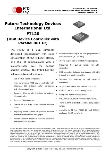
Future Technology Devices International Ltd. FT120 - FTDI
Future Technology Devices International Ltd. FT120 - FTDI
Future Technology Devices International Ltd. FT120 - FTDI

You also want an ePaper? Increase the reach of your titles
YUMPU automatically turns print PDFs into web optimized ePapers that Google loves.
<strong>Future</strong> <strong>Technology</strong> <strong>Devices</strong><br />
<strong>International</strong> <strong>Ltd</strong>.<br />
<strong>FT120</strong><br />
(USB Device Controller with<br />
Parallel Bus IC)<br />
The <strong>FT120</strong> is a USB controller<br />
developed independently with close<br />
consideration of the industry classic,<br />
D12 chip. It communicates with a<br />
microcontroller over the generic<br />
parallel interface. The <strong>FT120</strong> has the<br />
following advanced features:<br />
USB 2.0 Full Speed compatible.<br />
High performance USB device controller with<br />
integrated SIE, endpoint buffer, transceiver<br />
and voltage regulators.<br />
Supports 8-bit parallel interface to external<br />
microcontroller.<br />
Supports DMA operation<br />
Integrated 320 bytes of configurable endpoint<br />
buffer<br />
Ping-pong buffer scheme for primary endpoint<br />
increases data transfer throughput<br />
Multiple interrupt modes to facilitate both bulk<br />
and isochronous transfers.<br />
Document No.: FT_000646<br />
<strong>FT120</strong> USB DEVICE CONTROLLER WITH PARALLEL BUS IC<br />
Datasheet Version 1.0<br />
Clearance No.: <strong>FTDI</strong># 291<br />
Dedicated clock output pin with programmable<br />
clock frequency (4 – 24 MHz)<br />
30 kHz output clock provided during suspend.<br />
Integrated D+ pull-up resistor for USB<br />
connection<br />
USB connection indicator that toggles with USB<br />
transmit and receive activities.<br />
Supports bus powered or self powered<br />
application.<br />
Single power supply operation at 3.3V or 5V.<br />
Internal 1.8V and 3.3V LDO regulators<br />
Integrated power-on-reset circuit.<br />
UHCI/OHCI/EHCI host controller compatible.<br />
-40°C to 85°C extended operating temperature<br />
range.<br />
Available in Pb-free TSSOP-28 and QFN-28<br />
packages (RoHS compliant).<br />
Neither the whole nor any part of the information contained in, or the product described in this manual, may be adapted or reproduced<br />
in any material or electronic form without the prior written consent of the copyright holder. This product and its documentation are<br />
supplied on an as-is basis and no warranty as to their suitability for any particular purpose is either made or implied. <strong>Future</strong> <strong>Technology</strong><br />
<strong>Devices</strong> <strong>International</strong> <strong>Ltd</strong> will not accept any claim for damages howsoever arising as a result of use or failure of this product. Your<br />
statutory rights are not affected. This product or any variant of it is not intended for use in any medical appliance, device or system in<br />
which the failure of the product might reasonably be expected to result in personal injury. This document provides preliminary<br />
information that may be subject to change without notice. No freedom to use patents or other intellectual property rights is implied by<br />
the publication of this document. <strong>Future</strong> <strong>Technology</strong> <strong>Devices</strong> <strong>International</strong> <strong>Ltd</strong>, Unit 1, 2 Seaward Place, Centurion Business Park, Glasgow<br />
G41 1HH United Kingdom. Scotland Registered Company Number: SC136640<br />
Copyright © 2012 <strong>Future</strong> <strong>Technology</strong> <strong>Devices</strong> <strong>International</strong> Limited 1
1 Typical Applications<br />
Document No.: FT_000646<br />
<strong>FT120</strong> USB DEVICE CONTROLLER WITH PARALLEL BUS IC<br />
Datasheet Version 1.0<br />
Clearance No.: <strong>FTDI</strong># 291<br />
Provide USB port to Microcontrollers Provide USB port to FPGA’s<br />
USB Industrial Control<br />
Mass storage data transfers for multitude of<br />
embedded systems applications, including<br />
medical, industrial data-logger, power-<br />
metering, and test instrumentation<br />
1.1 Part Numbers<br />
Part Number Package<br />
Utilising USB to add system modularity<br />
Isochronous support for video applications in<br />
security, industrial control, and quality<br />
inspections<br />
<strong>FT120</strong>T-x TSSOP-28<br />
<strong>FT120</strong>Q-x QFN-28<br />
Note: Packaging codes for x is:<br />
- R: Taped and Reel, (TSSOP is 2,500pcs per reel, QFN is 6,000pcs per reel).<br />
- U: Tube packing, 50pcs per tube (TSSOP only)<br />
- T: Tray packing, 490pcs per tray (QFN only)<br />
For example: <strong>FT120</strong>T-R is 2,500pcs taped and reel packing<br />
1.2 USB Compliant<br />
At the time of writing this datasheet, the <strong>FT120</strong> was in the process of completing USB compliance<br />
testing.<br />
Copyright © 2012 <strong>Future</strong> <strong>Technology</strong> <strong>Devices</strong> <strong>International</strong> Limited 2
2 Block Diagrams<br />
Figure 2-1 <strong>FT120</strong> Block Diagram<br />
For a description of each function please refer to Section 4.<br />
Document No.: FT_000646<br />
<strong>FT120</strong> USB DEVICE CONTROLLER WITH PARALLEL BUS IC<br />
Datasheet Version 1.0<br />
Clearance No.: <strong>FTDI</strong># 291<br />
Copyright © 2012 <strong>Future</strong> <strong>Technology</strong> <strong>Devices</strong> <strong>International</strong> Limited 3
Table of Contents<br />
Document No.: FT_000646<br />
<strong>FT120</strong> USB DEVICE CONTROLLER WITH PARALLEL BUS IC<br />
Datasheet Version 1.0<br />
Clearance No.: <strong>FTDI</strong># 291<br />
1 Typical Applications ...................................................................... 2<br />
1.1 Part Numbers...................................................................................... 2<br />
1.2 USB Compliant .................................................................................... 2<br />
2 Block Diagrams ............................................................................ 3<br />
3 Device Pin Out and Signal Description .......................................... 6<br />
3.1 TSSOP-28 Package Pin Out ................................................................. 6<br />
3.2 QFN-28 Package Pin Out ..................................................................... 6<br />
3.3 Pin Description ................................................................................... 7<br />
4 Function Description..................................................................... 9<br />
4.1 Functional Block Descriptions ............................................................. 9<br />
4.2 Interrupt Modes ................................................................................ 10<br />
5 Endpoint Buffer Management ..................................................... 11<br />
6 Commands and Registers ........................................................... 13<br />
6.1 Command Summary .......................................................................... 13<br />
6.2 Initialization Commands ................................................................... 14<br />
6.2.1 Set Address Enable .................................................................................................... 14<br />
6.2.2 Set Endpoint Enable ................................................................................................... 14<br />
6.2.3 Set Mode .................................................................................................................. 15<br />
6.2.4 Set DMA ................................................................................................................... 16<br />
6.3 Data Flow Commands ....................................................................... 18<br />
6.3.1 Read Interrupt Register .............................................................................................. 18<br />
6.3.2 Select Endpoint ......................................................................................................... 19<br />
6.3.3 Read Last Transaction Status ...................................................................................... 19<br />
6.3.4 Read Endpoint Status ................................................................................................. 20<br />
6.3.5 Read Buffer ............................................................................................................... 21<br />
6.3.6 Write Buffer .............................................................................................................. 21<br />
6.3.7 Clear Buffer .............................................................................................................. 21<br />
6.3.8 Validate Buffer .......................................................................................................... 22<br />
6.3.9 Set Endpoint Status ................................................................................................... 22<br />
6.3.10 Acknowledge Setup ................................................................................................ 22<br />
6.4 General Commands ........................................................................... 22<br />
6.4.1 Read Current Frame Number ....................................................................................... 23<br />
6.4.2 Send Resume ............................................................................................................ 23<br />
7 Reference Schematic .................................................................. 24<br />
8 <strong>Devices</strong> Characteristics and Ratings ........................................... 25<br />
8.1 Absolute Maximum Ratings............................................................... 25<br />
8.2 DC Characteristics............................................................................. 26<br />
Copyright © 2012 <strong>Future</strong> <strong>Technology</strong> <strong>Devices</strong> <strong>International</strong> Limited 4
Document No.: FT_000646<br />
<strong>FT120</strong> USB DEVICE CONTROLLER WITH PARALLEL BUS IC<br />
Datasheet Version 1.0<br />
Clearance No.: <strong>FTDI</strong># 291<br />
8.3 AC Characteristics ............................................................................. 27<br />
9 Package Parameters ................................................................... 31<br />
9.1 TSSOP-28 Package Dimensions ........................................................ 31<br />
9.2 TSSOP-28 Package Markings ........................................................... 32<br />
9.3 QFN-28 Package Dimensions ............................................................ 33<br />
9.4 QFN-28 Package Markings ............................................................... 34<br />
9.5 Solder Reflow Profile ........................................................................ 35<br />
10 Contact Information ................................................................... 37<br />
Appendix A - List of Figures and Tables ..................................................... 38<br />
Appendix B - Revision History .................................................................... 40<br />
Copyright © 2012 <strong>Future</strong> <strong>Technology</strong> <strong>Devices</strong> <strong>International</strong> Limited 5
Document No.: FT_000646<br />
<strong>FT120</strong> USB DEVICE CONTROLLER WITH PARALLEL BUS IC<br />
Datasheet Version 1.0<br />
Clearance No.: <strong>FTDI</strong># 291<br />
3 Device Pin Out and Signal Description<br />
3.1 TSSOP-28 Package Pin Out<br />
Figure 3-1 TSSOP-28 package schematic symbol<br />
3.2 QFN-28 Package Pin Out<br />
Figure 3-2 QFN-28 package schematic symbol<br />
Copyright © 2012 <strong>Future</strong> <strong>Technology</strong> <strong>Devices</strong> <strong>International</strong> Limited 6
3.3 Pin Description<br />
PIN No.<br />
(TSSOP-<br />
28)<br />
PIN No.<br />
(QFN-<br />
28)<br />
Document No.: FT_000646<br />
<strong>FT120</strong> USB DEVICE CONTROLLER WITH PARALLEL BUS IC<br />
Datasheet Version 1.0<br />
Clearance No.: <strong>FTDI</strong># 291<br />
PIN NAME TYPE DESCRIPTION<br />
1 26 DATA0 IO Data bus bit 0.<br />
2 27 DATA1 IO Data bus bit 1.<br />
3 28 DATA2 IO Data bus bit 2.<br />
4 1 DATA3 IO Data bus bit 3.<br />
5 21 GND P Ground.<br />
6 2 DATA4 IO Data bus bit 4.<br />
7 3 DATA5 IO Data bus bit 5.<br />
8 4 DATA6 IO Data bus bit 6.<br />
9 5 DATA7 IO Data bus bit 7.<br />
10 6 ALE I Address latch enable for multiplexed address/data<br />
bus configuration.<br />
This pin must be pulled Low for non-multiplexed<br />
address/data bus configuration.<br />
11 7 CS_n I Chip select (Active Low).<br />
12 8 SUSPEND I,OD Device suspend (output) and wakeup (input).<br />
13 9 CLKOUT O Programmable output clock.<br />
14 10 INT_n OD Interrupt (Active Low).<br />
15 11 RD_n I Read enable (Active Low).<br />
16 12 WR_n I Write enable (Active Low).<br />
17 13 DMREQ O DMA request.<br />
18 14 DMACK_n I DMA acknowledge (Active Low).<br />
19 15 EOT_n I End of DMA transfer (Active Low). Also function<br />
as Vbus sensing input for self-powered<br />
application. _n_n_n_n<br />
20 16 RESET_n I Asynchronous reset (Active Low).<br />
21 17 GL_n OD USB bus activity indicator (Active Low)<br />
22 18 OSCI I Crystal connection input (6MHz); alternatively, a<br />
1.8V square wave clock can be applied.<br />
23 19 OSCO O<br />
Crystal connection output (6MHz) ; if the external<br />
clock signal is connected to OSCI, then OSCO<br />
Copyright © 2012 <strong>Future</strong> <strong>Technology</strong> <strong>Devices</strong> <strong>International</strong> Limited 7
PIN No.<br />
(TSSOP-<br />
28)<br />
PIN No.<br />
(QFN-<br />
28)<br />
Document No.: FT_000646<br />
<strong>FT120</strong> USB DEVICE CONTROLLER WITH PARALLEL BUS IC<br />
Datasheet Version 1.0<br />
Clearance No.: <strong>FTDI</strong># 291<br />
PIN NAME TYPE DESCRIPTION<br />
24 20 VCC P<br />
should be left unconnected<br />
Power supply (3.3V or 5V)<br />
25 22 USBDM AIO USB data signal minus<br />
26 23 USBDP AIO USB data signal plus<br />
27 24 VOUT3V3 P 3.3V regulator output for 5V operation;<br />
To operate the IC at 3.3 V, supply 3.3 V to both<br />
the VCC and VOUT3V3 pins<br />
28 25 A0 I Address bit for non-multiplexed address/data bus<br />
configuration.<br />
- A0=1 indicates command phase;<br />
- A0=0 indicates data phase.<br />
This pin must be pulled High for multiplexed<br />
address/data bus configuration.<br />
- 29 GND P Ground. Die pad for QFN-28 package.<br />
Table 3-1 <strong>FT120</strong> Pin Description<br />
Note, symbol used for pin TYPE:<br />
OD : Open Drain Output<br />
O : Output<br />
IO : Bi-directional Input and Output<br />
I : Plain input<br />
AIO : Analog Input and Output<br />
P : Power or ground<br />
Copyright © 2012 <strong>Future</strong> <strong>Technology</strong> <strong>Devices</strong> <strong>International</strong> Limited 8
4 Function Description<br />
Document No.: FT_000646<br />
<strong>FT120</strong> USB DEVICE CONTROLLER WITH PARALLEL BUS IC<br />
Datasheet Version 1.0<br />
Clearance No.: <strong>FTDI</strong># 291<br />
The <strong>FT120</strong> is a USB device controller which interfaces with microcontrollers via a generic 8-bit parallel<br />
bus.<br />
4.1 Functional Block Descriptions<br />
The following sections describe the function of each block. Please refer to the block diagram shown in<br />
Figure 2-1.<br />
+1.8V LDO Regulator. The +1.8V LDO regulator generates the +1.8V reference voltage for the internal<br />
core of the IC with input capabilities from 3.3V or 5V.<br />
+3.3V LDO Regulator. The +3.3V LDO regulator generates the +3.3V supply voltage for the USB<br />
transceiver. An external decoupling capacitor needs to be attached to the VOUT3V3 regulator output pin.<br />
The regulator also provides +3.3V power to the 1.5kΩ internal pull up resistor on USBDP pin. The<br />
allowable input voltages are 5V or 3.3V. When using 3.3V voltage as input voltage, the VCC and<br />
VOUT3V3 pins should be tied together. This will result in the regulator being by-passed.<br />
USB Transceiver. The USB Transceiver cell provides the USB 1.1 / USB 2.0 full-speed physical interface.<br />
Output drivers provide +3.3V level slew rate control , while a differential input and two single ended<br />
input receivers provide data in, Single-Ended-0 (SE0) and USB reset detection conditions respectfully. A<br />
1.5kΩ pull up resistor on USBDP is incorporated.<br />
DPLL. The DPLL cell locks on to the incoming NRZI USB data and generates recovered clock and data<br />
signals..<br />
Internal Oscillator. The Internal Oscillator cell generates a 6MHz reference clock from the 6MHz crystal.<br />
The Oscillator also has the capability of running from an external clock applied on the OSCI pin. This<br />
provides an input to the Clock Multiplier function.<br />
Clock Multiplier. The 12MHz and 48MHz reference clock signals for various internal blocks can be<br />
generated from the 6 MHz via the oscillator functions and clock multiplier circuitry.<br />
Serial Interface Engine (SIE). The Serial Interface Engine (SIE) block performs the parallel to serial<br />
and serial to parallel conversion of the USB data. In accordance with the USB 2.0 specification, it<br />
performs bit stuffing/un-stuffing and CRC5/CRC16 generation. It also checks the CRC on the USB data<br />
stream.<br />
Copyright © 2012 <strong>Future</strong> <strong>Technology</strong> <strong>Devices</strong> <strong>International</strong> Limited 9
Document No.: FT_000646<br />
<strong>FT120</strong> USB DEVICE CONTROLLER WITH PARALLEL BUS IC<br />
Datasheet Version 1.0<br />
Clearance No.: <strong>FTDI</strong># 291<br />
USB Protocol Engine. The USB Protocol Engine manages the data stream from the device USB control<br />
endpoint. It handles the low level USB protocol requests generated by the USB host controller. The<br />
Protocol Engine also includes a memory management unit which handles endpoint buffers.<br />
OUT Buffer. Data sent from the USB host controller to <strong>FT120</strong> via the USB data OUT endpoint is stored in<br />
the OUT buffer. Data is removed from the OUT buffer to system memory under control of the parallel<br />
interface block.<br />
IN Buffer. Data from system memory is stored in the IN buffer. The USB host controller removes data<br />
from the IN buffer by sending a USB request for data from the device data IN endpoint.<br />
RESET Generator. The integrated Reset Generator cell provides a reliable power-on reset to the device<br />
internal circuitry at power up. The RESET_n input pin allows an external device to reset the <strong>FT120</strong>.<br />
Parallel Interface Block. The 8-bit parallel bus allows direct interface to a generic microcontroller<br />
(MCU), supporting both multiplexed and non-multiplexed address/data bus configurations. The <strong>FT120</strong><br />
also supports Direct Memory Access (DMA) operation. With DMA access data can be written to the IN<br />
buffer or read from the OUT buffer without MCU intervention. The DMA access can be done in single cycle<br />
or burst mode.<br />
4.2 Interrupt Modes<br />
The <strong>FT120</strong> interrupt pin (INT_n) can be programmed to generate interrupt in different modes. The<br />
interrupt source can be any bit in Interrupt Register, or receiving SOF packet, or both. The interrupt<br />
modes are selectable by two register bits, one is the SOF-only Interrupt Mode bit (bit 7 of Clock Division<br />
Factor register), and the other is Interrupt Pin Mode bit (bit 5 of DMA Configuration register).<br />
Interrupt<br />
mode<br />
Bit SOF-only<br />
Interrupt<br />
Mode<br />
Bit Interrupt<br />
Pin Mode<br />
Interrupt source<br />
0 0 0 Any bit in Interrupt register<br />
1 0 1 Any bit in Interrupt register and SOF<br />
2 1 X SOF only<br />
Table 4-1 Interrupt modes<br />
Copyright © 2012 <strong>Future</strong> <strong>Technology</strong> <strong>Devices</strong> <strong>International</strong> Limited 10
Document No.: FT_000646<br />
<strong>FT120</strong> USB DEVICE CONTROLLER WITH PARALLEL BUS IC<br />
Datasheet Version 1.0<br />
Clearance No.: <strong>FTDI</strong># 291<br />
5 Endpoint Buffer Management<br />
The <strong>FT120</strong> has 3 physical endpoints (EP0, EP1 and EP2) or 6 logic endpoints (EPI0-EPI5). EP0 is control<br />
endpoint, with 16 bytes maximum packet size for both control OUT (EPI0) and control IN (EPI1)<br />
endpoint. EP1 can be used as either bulk endpoint or interrupt endpoint, with 16 bytes maximum packet<br />
size for both OUT (EPI2) and IN (EPI3) endpoints. Table 5-1 shows the endpoint type and maximum<br />
packet size for EP0 and EP1.<br />
Endpoint<br />
Number<br />
0<br />
1<br />
Endpoint<br />
Index (EPI)<br />
0<br />
1<br />
2<br />
3<br />
Endpoint<br />
Direction<br />
OUT<br />
IN<br />
OUT<br />
Table 5-1 Endpoint configuration for EP0 and EP1<br />
IN<br />
Transfer Type Max Packet Size<br />
Control<br />
Control<br />
Bulk/Interrupt<br />
Bulk/Interrupt<br />
EP2 is the primary endpoint. It can be configured as either bulk/interrupt or isochronous endpoint. The<br />
maximum packet size allowed for EP2 depends on the mode of configuration through Set Mode<br />
command. Table 5-2 shows all the 4 endpoint configuration modes for EP2.<br />
Endpoint<br />
Configuration<br />
Mode (EP2)<br />
0<br />
(default)<br />
Endpoint<br />
Index (EPI)<br />
4<br />
5<br />
Endpoint<br />
Direction<br />
OUT<br />
IN<br />
Copyright © 2012 <strong>Future</strong> <strong>Technology</strong> <strong>Devices</strong> <strong>International</strong> Limited 11<br />
16<br />
16<br />
16<br />
16<br />
Transfer Type Max Packet Size<br />
Bulk/Interrupt<br />
Bulk/Interrupt<br />
1 4 OUT Isochronous 128<br />
2 5 IN Isochronous 128<br />
3 4<br />
5<br />
OUT<br />
IN<br />
Table 5-2 Endpoint configuration for EP2<br />
Isochronous<br />
Isochronous<br />
As the primary endpoint, EP2 is suitable for transmitting or receiving relatively large data. To improve the<br />
data throughput, a pair of ping-pong buffer is implemented for EP2 buffer. This allows the concurrent<br />
operation between USB bus access and MCU or DMA local bus access. For example, for EP2 IN endpoint<br />
(EPI5), the USB host can read data from <strong>FT120</strong> ping buffer while the local MCU is writing to the pong<br />
buffer at the same time. The USB host can subsequently read from <strong>FT120</strong> pong buffer without waiting for<br />
it to be filled. Buffer switching is handled automatically by <strong>FT120</strong>.<br />
64<br />
64<br />
64<br />
64
Document No.: FT_000646<br />
<strong>FT120</strong> USB DEVICE CONTROLLER WITH PARALLEL BUS IC<br />
Datasheet Version 1.0<br />
Clearance No.: <strong>FTDI</strong># 291<br />
The EP2 buffer also supports DMA operation. The MCU needs to initialize the DMA operation through Set<br />
DMA command. Once DMA operation is enabled, data will be moving between the system memory and<br />
<strong>FT120</strong> endpoint buffer under the DMA controller. Buffer switching between ping buffer and pong buffer is<br />
handled automatically.<br />
Copyright © 2012 <strong>Future</strong> <strong>Technology</strong> <strong>Devices</strong> <strong>International</strong> Limited 12
Document No.: FT_000646<br />
<strong>FT120</strong> USB DEVICE CONTROLLER WITH PARALLEL BUS IC<br />
Datasheet Version 1.0<br />
Clearance No.: <strong>FTDI</strong># 291<br />
6 Commands and Registers<br />
The <strong>FT120</strong> supported commands are summarized in Table 6-1. These commands include initialization<br />
commands, data flow commands and generic commands, which are described in detail in sections 6.2,<br />
6.3 and 6.4 respectively.<br />
6.1 Command Summary<br />
Command Name Target Code (hex) Data phase<br />
Initialization Commands<br />
Set Address Enable Device D0h Write 1 byte<br />
Set Endpoint Enable Device D8h Write 1 byte<br />
Set Mode Device F3h Write 2 bytes<br />
Set DMA Device FBh Write/Read 1 byte<br />
Data Flow Commands<br />
Read Interrupt Register Device F4h Read 2 bytes<br />
Select Endpoint Endpoint 0 OUT 00h Read 1 byte (optional)<br />
Endpoint 0 IN 01h Read 1 byte (optional)<br />
Endpoint 1 OUT 02h Read 1 byte (optional)<br />
Endpoint 1 IN 03h Read 1 byte (optional)<br />
Endpoint 2 OUT 04h Read 1 byte (optional)<br />
Endpoint 2 IN 05h Read 1 byte (optional)<br />
Read Last Transaction Status Endpoint 0 OUT 40h Read 1 byte<br />
Endpoint 0 IN 41h Read 1 byte<br />
Endpoint 1 OUT 42h Read 1 byte<br />
Endpoint 1 IN 43h Read 1 byte<br />
Endpoint 2 OUT 44h Read 1 byte<br />
Endpoint 2 IN 45h Read 1 byte<br />
Read Endpoint Status Endpoint 0 OUT 80h Read 1 byte<br />
Endpoint 0 IN 81h Read 1 byte<br />
Endpoint 1 OUT 82h Read 1 byte<br />
Endpoint 1 IN 83h Read 1 byte<br />
Endpoint 2 OUT 84h Read 1 byte<br />
Copyright © 2012 <strong>Future</strong> <strong>Technology</strong> <strong>Devices</strong> <strong>International</strong> Limited 13
Document No.: FT_000646<br />
<strong>FT120</strong> USB DEVICE CONTROLLER WITH PARALLEL BUS IC<br />
Datasheet Version 1.0<br />
Clearance No.: <strong>FTDI</strong># 291<br />
Command Name Target Code (hex) Data phase<br />
Endpoint 2 IN 85h Read 1 byte<br />
Read Buffer Selected Endpoint F0h Read multiple bytes<br />
Write Buffer Selected Endpoint F0h Write multiple bytes<br />
Set Endpoint Status Endpoint 0 OUT 40h Write 1 byte<br />
Endpoint 0 IN 41h Write 1 byte<br />
Endpoint 1 OUT 42h Write 1 byte<br />
Endpoint 1 IN 43h Write 1 byte<br />
Endpoint 2 OUT 44h Write 1 byte<br />
Endpoint 2 IN 45h Write 1 byte<br />
Acknowledge Setup Selected Endpoint F1h None<br />
Clear Buffer Selected Endpoint F2h None<br />
Validate Buffer Selected Endpoint FAh None<br />
General Commands<br />
Read Current Frame Number Device F5h Read 1 or 2 bytes<br />
Send Resume Device F6h None<br />
Table 6-1 <strong>FT120</strong> command set<br />
6.2 Initialization Commands<br />
6.2.1 Set Address Enable<br />
Command : D0h<br />
Data : Write 1 byte<br />
Bit Symbol Reset Description<br />
6-0 Address 0b’0000000 USB assigned device address. A bus reset will reset all<br />
address bits to 0.<br />
7 Enable 0 Function enable. A bus reset will automatically enable the<br />
function at default address 0.<br />
Table 6-2 Address Enable Register<br />
6.2.2 Set Endpoint Enable<br />
Command : D8h<br />
Copyright © 2012 <strong>Future</strong> <strong>Technology</strong> <strong>Devices</strong> <strong>International</strong> Limited 14
Data : Write 1 byte<br />
Document No.: FT_000646<br />
<strong>FT120</strong> USB DEVICE CONTROLLER WITH PARALLEL BUS IC<br />
Datasheet Version 1.0<br />
Clearance No.: <strong>FTDI</strong># 291<br />
Bit Symbol Reset Description<br />
0 EP_Enable 0 Enable EP1 and EP2 endpoints (Note EP0 is always<br />
enabled regardless the setting of EP_Enable bit).<br />
Endpoints can only be enabled when the function is<br />
enabled.<br />
7-1 Reserved 0b’0000000 Reserved, write to 0<br />
Table 6-3 Endpoint Enable Register<br />
6.2.3 Set Mode<br />
Command : F3h<br />
Data : Write 2 bytes<br />
Bit Symbol Reset Description<br />
0 Reserved 0 Reserved, write to 0<br />
1 No Suspend Clock 1 0: CLKOUT switches to 30 KHz during USB suspend<br />
1: CLKOUT remains unchanged during USB suspend<br />
Note: The programmed value will not be changed by a<br />
bus reset.<br />
2 Clock Running 1 0: internal clocks stop during USB suspend<br />
1: internal clocks continue running during USB suspend<br />
This bit must be set to ‘0’ for bus powered application in<br />
order to meet the USB suspend current requirement.<br />
Note: The programmed value will not be changed by a<br />
bus reset.<br />
3 Interrupt Mode 1 0: interrupt will not generate on NAK or Error<br />
transactions<br />
1: interrupt will generate on NAK and Error transactions<br />
Note: The programmed value will not be changed by a<br />
bus reset.<br />
4 DP_Pullup 0 0: Pullup resistor on USBDP pin disabled<br />
5 Reserved 0 Reserved, write to 0<br />
7-6 Endpoint Configuration<br />
Mode<br />
1: Pullup resistor on USBDP pin enabled when Vbus is<br />
present<br />
Note: The programmed value will not be changed by a<br />
bus reset.<br />
0b’00 Set the endpoint configuration mode for EP2.<br />
00: Mode 0 (Non-ISO Mode)<br />
01: Mode 1 (ISO-OUT Mode)<br />
10: Mode 2 (ISO-IN Mode)<br />
Copyright © 2012 <strong>Future</strong> <strong>Technology</strong> <strong>Devices</strong> <strong>International</strong> Limited 15
Document No.: FT_000646<br />
<strong>FT120</strong> USB DEVICE CONTROLLER WITH PARALLEL BUS IC<br />
Datasheet Version 1.0<br />
Clearance No.: <strong>FTDI</strong># 291<br />
Bit Symbol Reset Description<br />
Table 6-4 Configuration Register (Byte 1)<br />
11: Mode 3 (ISO-IO Mode)<br />
Bit Symbol Reset Description<br />
3-0 Clock Division Factor 0b’1011 The Clock Division Factor value (CDF) determines the<br />
output clock frequency on the CLKOUT pin. Frequency =<br />
48 MHz / (CDF +1), where CDF ranges 1-12 or the<br />
allowed CLKOUT frequency is 4-24 MHz. Default CLKOUT<br />
is 4 MHz.<br />
5-4 Reserved 0b’00 Reserved, write to 0<br />
6 SET_TO_ONE 0 This bit must be set to 1<br />
7 SOF-only Interrupt<br />
Mode<br />
Table 6-5 Clock Division Factor Register (Byte 2)<br />
6.2.4 Set DMA<br />
Command : FBh<br />
Data : Read/Write 1 byte<br />
When the CDF is programmed to 0b’1111, the CLKOUT<br />
will be turned off. It is recommended to turn off the<br />
CLKOUT if it not used, for power saving (about 3mA).<br />
Note: The programmed value will not be changed by a<br />
bus reset.<br />
0 0: normal operation<br />
1: interrupt will generate on receiving SOF packet only,<br />
regardless the value of the Interrupt Pin Mode bit in DMA<br />
configuration register.<br />
Bit Symbol Reset Description<br />
1-0 DMA Burst 0b’00 Set the DMA burst size<br />
00: Single cycle mode<br />
01: 4 cycle burst mode<br />
10: 8 cycle burst mode<br />
11: 16 cycle burst mode<br />
2 DMA Enable 0 Enable DMA operation<br />
0: DMA operation is disabled<br />
1: DMA operation is enabled<br />
<strong>FT120</strong> will clear this bit upon EOT_n assertion.<br />
3 DMA Direction 0 This bit indicates the DMA read or write operation.<br />
0: DMA read. Data read from <strong>FT120</strong> OUT buffer to<br />
system memory.<br />
1: DMA write. Data write to <strong>FT120</strong> IN buffer from system<br />
Copyright © 2012 <strong>Future</strong> <strong>Technology</strong> <strong>Devices</strong> <strong>International</strong> Limited 16
Document No.: FT_000646<br />
<strong>FT120</strong> USB DEVICE CONTROLLER WITH PARALLEL BUS IC<br />
Datasheet Version 1.0<br />
Clearance No.: <strong>FTDI</strong># 291<br />
Bit Symbol Reset Description<br />
memory.<br />
4 Auto Reload 0 Automatically restart the DMA operation.<br />
0: DMA needs to restart by software<br />
1: DMA will restart automatically after the previous DMA<br />
transfer finishes<br />
5 Interrupt Pin Mode 0 0: normal operation. Interrupt will generate if any of the<br />
bit in the interrupt register is set.<br />
1: interrupt will generate upon receiving SOF packet or if<br />
any of the bit in the interrupt register is set.<br />
6 EPI4 Interrupt Enable 0 Interrupt Enable for endpoint index 4. During DMA<br />
operation, EPI4 interrupt should be turned off to avoid<br />
un-necessary interrupt service.<br />
7 EPI5 Interrupt Enable 0 Interrupt Enable for endpoint index 5. During DMA<br />
operation, EPI5 interrupt should be turned off to avoid<br />
un-necessary interrupt service.<br />
Table 6-6 DMA Configuration Register<br />
Copyright © 2012 <strong>Future</strong> <strong>Technology</strong> <strong>Devices</strong> <strong>International</strong> Limited 17
6.3 Data Flow Commands<br />
6.3.1 Read Interrupt Register<br />
Command : F4h<br />
Data : Read 1 or 2 bytes<br />
Document No.: FT_000646<br />
<strong>FT120</strong> USB DEVICE CONTROLLER WITH PARALLEL BUS IC<br />
Datasheet Version 1.0<br />
Clearance No.: <strong>FTDI</strong># 291<br />
Bit Symbol Reset Description<br />
0 Endpoint 0 Out 0 Interrupt for endpoint 0 OUT buffer. Cleared by Read<br />
Last Transaction Status command.<br />
1 Endpoint 0 In 0 Interrupt for endpoint 0 IN buffer. Cleared by Read Last<br />
Transaction Status command.<br />
2 Endpoint 1 Out 0 Interrupt for endpoint 1 OUT buffer. Cleared by Read<br />
Last Transaction Status command.<br />
3 Endpoint 1 In 0 Interrupt for endpoint 1 IN buffer. Cleared by Read Last<br />
Transaction Status command.<br />
4 Endpoint 2 Out 0 Interrupt for endpoint 2 OUT buffer. Cleared by Read<br />
Last Transaction Status command.<br />
5 Endpoint 2 In 0 Interrupt for endpoint 2 IN buffer. Cleared by Read Last<br />
Transaction Status command.<br />
6 Bus Reset 0 Interrupt for bus reset. This bit will be cleared after<br />
reading.<br />
7 Suspend Change 0 Interrupt for USB bus suspend status change. This bit<br />
will be set to ‘1’ when <strong>FT120</strong> goes to suspend (missing 3<br />
continuous SOFs) or resumes from suspend. This bit will<br />
be cleared after reading.<br />
Table 6-7 Interrupt Register Byte 1<br />
Bit Symbol Reset Description<br />
0 DMA EOT 0 Interrupt for end of DMA transfer. This bit will be cleared<br />
after reading.<br />
1 Reserved 0b’xxxxxxx Reserved<br />
Table 6-8 Interrupt Register Byte 2<br />
Copyright © 2012 <strong>Future</strong> <strong>Technology</strong> <strong>Devices</strong> <strong>International</strong> Limited 18
6.3.2 Select Endpoint<br />
Document No.: FT_000646<br />
<strong>FT120</strong> USB DEVICE CONTROLLER WITH PARALLEL BUS IC<br />
Datasheet Version 1.0<br />
Clearance No.: <strong>FTDI</strong># 291<br />
Command : 00-05h (0ih where ‘i’ is the index of logic endpoint number)<br />
Data : Optional Read 1 byte<br />
Bit Symbol Reset Description<br />
0 Full/Empty 0 0: selected endpoint buffer is empty<br />
1: selected endpoint buffer is full<br />
1 Stall 0 0: selected endpoint is not stalled<br />
7-2 Reserved 0b’xxxxxx Reserved<br />
Table 6-9 Endpoint Status Register<br />
6.3.3 Read Last Transaction Status<br />
1: selected endpoint is stalled<br />
Command : 40-45h (4ih where ‘i’ is the index of logic endpoint number)<br />
Data : Read 1 byte<br />
Bit Symbol Reset Description<br />
0 Data Receive/Transmit<br />
Success<br />
4-1 Error Code 0b’0000 Refer to Table 6-11<br />
0 0: indicate USB data receive or transmit not OK<br />
1: indicate USB data receive or transmit OK<br />
5 Setup Packet 0 0: indicate not a setup packet<br />
1: indicate last received packet has a SETUP token<br />
6 Data 0/1 Packet 0 0: packet has a DATA0 token<br />
7 Previous Status not<br />
Read<br />
Table 6-10 Endpoint Last Transaction Status Register<br />
Error Code Result<br />
0000 No error<br />
0001 PID encoding error<br />
1: packet has a DATA1 token<br />
0 0: previous transaction status was read<br />
0: previous transaction status was not read<br />
Copyright © 2012 <strong>Future</strong> <strong>Technology</strong> <strong>Devices</strong> <strong>International</strong> Limited 19
Error Code Result<br />
0010 PID unknown<br />
0011 Unexpected packet<br />
0100 Token CRC error<br />
0101 Data CRC error<br />
0110 Time out error<br />
0111 Reserved<br />
1000 Unexpected EOP<br />
1001 Packet NAKed<br />
1010 Sent stall<br />
1011 Buffer overflow<br />
1101 Bit stuff error<br />
1111 Wrong DATA PID<br />
Table 6-11 Transaction error code<br />
6.3.4 Read Endpoint Status<br />
Document No.: FT_000646<br />
<strong>FT120</strong> USB DEVICE CONTROLLER WITH PARALLEL BUS IC<br />
Datasheet Version 1.0<br />
Clearance No.: <strong>FTDI</strong># 291<br />
Command : 80-85h (8ih where ‘i’ is the index of logic endpoint number)<br />
Data : Read 1 byte<br />
Bit Symbol Reset Description<br />
1-0 Reserved 0b’00 Reserved<br />
2 Setup packet 0 0: indicate not a setup packet<br />
4-3 Reserved 0b’xx Reserved<br />
1: indicate last received packet has a SETUP token<br />
5 Buffer 0 Full 0 0: ping buffer is not filled up<br />
1: ping buffer is filled up<br />
6 Buffer 1 Full 0 0: pong buffer is not filled up<br />
1: pong buffer is filled up<br />
Note: this bit only applicable to EP2 which supports pingpong<br />
buffer<br />
Copyright © 2012 <strong>Future</strong> <strong>Technology</strong> <strong>Devices</strong> <strong>International</strong> Limited 20
Document No.: FT_000646<br />
<strong>FT120</strong> USB DEVICE CONTROLLER WITH PARALLEL BUS IC<br />
Datasheet Version 1.0<br />
Clearance No.: <strong>FTDI</strong># 291<br />
Bit Symbol Reset Description<br />
7 Endpoint Stalled 0 0: endpoint is not stalled<br />
Table 6-12 Endpoint Buffer Status Register<br />
6.3.5 Read Buffer<br />
Command : F0h<br />
Data : Read multiple bytes<br />
1: endpoint is stalled<br />
The Read Buffer command is used to read the received packet from the selected endpoint OUT buffer.<br />
The data in the endpoint buffer is organized as follows:<br />
o byte 0: reserved, don’t care<br />
o byte 1: length of payload packet<br />
o byte 2: Payload packet byte 1<br />
o byte 3: Payload packet byte 2<br />
o …<br />
o byte n: Payload packet byte n (n = packet length + 2)<br />
For DMA read operation the first two bytes are skipped. Only the payload packet itself will be read and<br />
stored in system memory.<br />
6.3.6 Write Buffer<br />
Command : F0h<br />
Data : Write multiple bytes<br />
The Write Buffer command is used to write payload packet to the selected endpoint IN buffer.<br />
The data must be organized in the same way as described in the Read Buffer command. Byte 0 should<br />
always be set to 00h.<br />
For DMA write operation the first two bytes are skipped. Only the payload packet itself shall be written to<br />
the selected endpoint OUT buffer. Buffer is validated when the max packet size is reached, or when the<br />
DMA transfer is terminated by EOT_n (usually the last packet).<br />
6.3.7 Clear Buffer<br />
Command : F2h<br />
Data : None<br />
Copyright © 2012 <strong>Future</strong> <strong>Technology</strong> <strong>Devices</strong> <strong>International</strong> Limited 21
Document No.: FT_000646<br />
<strong>FT120</strong> USB DEVICE CONTROLLER WITH PARALLEL BUS IC<br />
Datasheet Version 1.0<br />
Clearance No.: <strong>FTDI</strong># 291<br />
Followed by Read Buffer command, the Clear Buffer command should be issued after all data has been<br />
read out from the endpoint buffer. This is to free the buffer to receive next packet from USB host.<br />
6.3.8 Validate Buffer<br />
Command : FAh<br />
Data : None<br />
Followed by Write Buffer command, the Validate Buffer command should be issued after all data has been<br />
written to the endpoint buffer. This is to set the buffer full flag so that the packet can be sent to USB host<br />
when IN token arrives.<br />
6.3.9 Set Endpoint Status<br />
Command : 40-45h (4ih where ‘i’ is the index of logic endpoint number)<br />
Data : Write 1 byte<br />
Bit Symbol Reset Description<br />
0 Stall 0 0: Disable the endpoint STALL state.<br />
7-1 Reserved 0b’xxxxxxx Reserved<br />
Table 6-13 Endpoint Control Register<br />
6.3.10 Acknowledge Setup<br />
Command : F1h<br />
Data : None<br />
1: Enable the endpoint STALL state.<br />
For EP0 OUT (control OUT endpoint) the STALL state will<br />
automatically be cleared by receiving a SETUP packet.<br />
When this bit is cleared, the endpoint will reinitialize. Any<br />
data in the endpoint buffer will be flushed away, and the<br />
PID for next packet will carry DATA0 flag.<br />
When receiving a SETUP packet the <strong>FT120</strong> will flush the IN buffer and disable the Validate Buffer and<br />
Clear Buffer commands for both IN and OUT endpoints. The MCU shall read and process the SETUP<br />
packet, and then issue the Acknowledge Setup command to re-enable the Validate Buffer and Clear<br />
Buffer commands. The Acknowledge Setup command must be sent to both IN and OUT endpoints.<br />
6.4 General Commands<br />
Copyright © 2012 <strong>Future</strong> <strong>Technology</strong> <strong>Devices</strong> <strong>International</strong> Limited 22
Document No.: FT_000646<br />
<strong>FT120</strong> USB DEVICE CONTROLLER WITH PARALLEL BUS IC<br />
Datasheet Version 1.0<br />
Clearance No.: <strong>FTDI</strong># 291<br />
6.4.1 Read Current Frame Number<br />
Command : F5h<br />
Data : Read One or Two Bytes<br />
Bit Symbol Reset Description<br />
7-0 Frame Number LSB 00h Frame number for last received SOF, byte 1 (least<br />
significant byte)<br />
Table 6-14 Frame Number LSB Register<br />
Bit Symbol Reset Description<br />
2-0 Frame Number MSB 0b’000 Frame number for last received SOF, byte 2 (Most<br />
significant byte)<br />
7-3 Reserved 0b’00000 Reserved<br />
Table 6-15 Frame Number MSB Register<br />
6.4.2 Send Resume<br />
Command : F6h<br />
Data : None<br />
To perform remote-wakeup when suspended, the MCU needs to issue Send Resume command. The<br />
<strong>FT120</strong> will send an upstream resume signal for a period of 10 ms. If the clock is not running during<br />
suspend, the MCU needs to wakeup <strong>FT120</strong> by drive SUSPEND pin to LOW, followed by Send Resume<br />
command.<br />
Copyright © 2012 <strong>Future</strong> <strong>Technology</strong> <strong>Devices</strong> <strong>International</strong> Limited 23
7 Reference Schematic<br />
Document No.: FT_000646<br />
<strong>FT120</strong> USB DEVICE CONTROLLER WITH PARALLEL BUS IC<br />
Datasheet Version 1.0<br />
Clearance No.: <strong>FTDI</strong># 291<br />
Figure 7-1 shows a reference schematic for a <strong>FT120</strong> module which can be connected to a generic<br />
microcontroller to add USB device function. The reference design supports both bus-powered and selfpowered<br />
application.<br />
Figure 7-1 <strong>FT120</strong> Reference schematics<br />
Copyright © 2012 <strong>Future</strong> <strong>Technology</strong> <strong>Devices</strong> <strong>International</strong> Limited 24
Document No.: FT_000646<br />
<strong>FT120</strong> USB DEVICE CONTROLLER WITH PARALLEL BUS IC<br />
Datasheet Version 1.0<br />
Clearance No.: <strong>FTDI</strong># 291<br />
8 <strong>Devices</strong> Characteristics and Ratings<br />
8.1 Absolute Maximum Ratings<br />
The absolute maximum ratings for the <strong>FT120</strong> devices are as follows. These are in accordance with the<br />
Absolute Maximum Rating System (IEC 60134). Exceeding these may cause permanent damage to the<br />
device.<br />
Parameter Value Unit<br />
Storage Temperature -65 to 150 °C<br />
Floor Life (Out of Bag) At Factory Ambient<br />
(30°C / 60% Relative Humidity)<br />
Copyright © 2012 <strong>Future</strong> <strong>Technology</strong> <strong>Devices</strong> <strong>International</strong> Limited 25<br />
168<br />
(IPC/JEDEC J-STD-033A MSL Level 3<br />
Compliant)*<br />
Ambient Temperature (Power Applied) -40 to 85 °C<br />
Hours<br />
Latch-up current TBD mA<br />
Electrostatic Discharge Voltage(ESD)<br />
human body model(HBM)<br />
Electrostatic Discharge Voltage(ESD)<br />
machine model(MM)<br />
Electrostatic Discharge Voltage(ESD)<br />
charged device model(CDM)<br />
±2000 V<br />
±200 V<br />
±500 V<br />
VCC Supply Voltage -0.5 to +6.0 V<br />
DC Input Voltage – USBDP and USBDM -0.5 to +3.8 V<br />
DC Input Voltage – High Impedance<br />
Bidirectional<br />
-0.5 to + (VCC +0.5) V<br />
DC Input Voltage – All Other Inputs -0.5 to + (VCC +0.5) V<br />
DC Output Current – Outputs 22 mA<br />
Table 8-1 Absolute Maximum Ratings<br />
* If devices are stored out of the packaging beyond this time limit the devices should be baked before<br />
use. The devices should be ramped up to a temperature of +125°C and baked for up to 17 hours.
8.2 DC Characteristics<br />
DC Characteristics (Ambient Temperature = -40°C to +85°C)<br />
Document No.: FT_000646<br />
<strong>FT120</strong> USB DEVICE CONTROLLER WITH PARALLEL BUS IC<br />
Datasheet Version 1.0<br />
Clearance No.: <strong>FTDI</strong># 291<br />
Parameter Description Minimum Typical Maximum Units Conditions<br />
VCC1<br />
VCC2<br />
Icc1<br />
Icc2<br />
Icc3<br />
VCC Operating Supply<br />
Voltage<br />
VCC Operating Supply<br />
Voltage<br />
Operating Supply<br />
Current<br />
Operating Supply<br />
Current<br />
Operating Supply<br />
Current<br />
4.0 5.0 5.5 V Normal Operation<br />
3.0 3.3 3.6 V<br />
5 mA<br />
8 mA<br />
84 μA<br />
Regulator by-pass<br />
mode Operation<br />
Normal Operation,<br />
USB bus transmit<br />
or receive,<br />
CLKOUT off<br />
Normal Operation,<br />
USB bus transmit<br />
or receive,<br />
CLKOUT = 12 MHz<br />
USB Suspend,<br />
Clock Running =<br />
‘0’, excluding the<br />
DP_Pullup current<br />
VOUT3V3 3.3v regulator output 3.0 3.3 3.6 V VCC=5V<br />
Table 8-2 Operating Voltage and Current<br />
Parameter Description Minimum Typical Maximum Units Conditions<br />
Voh Output Voltage High 2.4 3.6 V I source = 4mA<br />
Vol Output Voltage Low 0.4 V I sink = 4mA<br />
Vih Input Voltage High 2.0 V<br />
Vil Input Voltage Low - 0.8 V<br />
Table 8-3 digital I/O Pin Characteristics<br />
Parameter Description Minimum Typical Maximum Units Conditions<br />
UVoh<br />
UVol<br />
UVse<br />
UCom<br />
I/O Pins Static Output<br />
(High)<br />
I/O Pins Static Output<br />
(Low)<br />
Single Ended Rx<br />
Threshold<br />
Differential Common<br />
Mode<br />
2.8 3.6 V<br />
R L = 1.5kΩ to 3.6<br />
V<br />
- 0.3 V R L = 15kΩ to GND<br />
0.8 2.0 V<br />
0.8 2.5 V<br />
Copyright © 2012 <strong>Future</strong> <strong>Technology</strong> <strong>Devices</strong> <strong>International</strong> Limited 26
Document No.: FT_000646<br />
<strong>FT120</strong> USB DEVICE CONTROLLER WITH PARALLEL BUS IC<br />
Datasheet Version 1.0<br />
Clearance No.: <strong>FTDI</strong># 291<br />
Parameter Description Minimum Typical Maximum Units Conditions<br />
UVDif<br />
UDrvZ<br />
Differential Input<br />
Sensitivity<br />
Driver Output<br />
Impedance<br />
0.2 V<br />
29 - 44 Ω<br />
Table 8-4 USB I/O Pin (USBDP, USBDM) Characteristics<br />
8.3 AC Characteristics<br />
Parameter<br />
Frequency of Operation<br />
(see Note 1)<br />
Value<br />
Minimum Typical Maximum<br />
Including external<br />
22 Ω ±1% series<br />
resistor<br />
Unit<br />
5.997 6.000 6.003 MHz<br />
Duty Cycle 45 50 55 %<br />
Table 8-5 Crystal or clock Characteristics (OSCI, OSCO pins)<br />
Note 1: Equivalent to ±500ppm<br />
Symbol Parameter Min Max Unit<br />
ALE Timings:<br />
tLH ALE High Pulse Width 20 ns<br />
tAVLL Address Valid to ALE Low Time 10 ns<br />
tLLAX ALE Low to Address Transition Time 10 ns<br />
Write Timings:<br />
tCLWL CS_n (DMACK_n) Low to WR_n Low Time 0 ns<br />
tWHCH WR_n High to CS_n (DMACK_n) High Time 5 ns<br />
tAVWL A0 Valid to WR_n Low Time 0 ns<br />
tWHAX WR_n High to A0 Transition Time 5 ns<br />
tWL WR_n Low Pulse Width 20 ns<br />
tWDSU Write Data Setup Time 30 ns<br />
tWDH Write Data Hold Time 10 ns<br />
tWC Write Cycle Time 500 ns<br />
Copyright © 2012 <strong>Future</strong> <strong>Technology</strong> <strong>Devices</strong> <strong>International</strong> Limited 27
Document No.: FT_000646<br />
<strong>FT120</strong> USB DEVICE CONTROLLER WITH PARALLEL BUS IC<br />
Datasheet Version 1.0<br />
Clearance No.: <strong>FTDI</strong># 291<br />
Symbol Parameter Min Max Unit<br />
t(WC-WD) Write command to write data 600 ns<br />
Read Timings:<br />
tCLRL CS_n (DMACK_n) Low to RD_n Low Time 0 ns<br />
tRHCH RD_n High to CS_n (DMACK_n) High Time 5 ns<br />
tAVRL A0 Valid to RD_n Low Time 0 ns<br />
tRL RD_n Low Pulse Width 20 ns<br />
tRLDD RD_n Low to Data Valid Time 20 ns<br />
tRHDZ RD_n High to Data Hi-Z Time 20 ns<br />
tRC Read Cycle Time 500 ns<br />
t(WC-RD) Write command to read data 600 ns<br />
Table 8-6 Parallel Interface IO timing<br />
Figure 8-1 ALE Timing<br />
Copyright © 2012 <strong>Future</strong> <strong>Technology</strong> <strong>Devices</strong> <strong>International</strong> Limited 28
Figure 8-2 Parallel interface timing<br />
Document No.: FT_000646<br />
<strong>FT120</strong> USB DEVICE CONTROLLER WITH PARALLEL BUS IC<br />
Datasheet Version 1.0<br />
Clearance No.: <strong>FTDI</strong># 291<br />
Symbol Parameter Min Max Unit<br />
Single-cycle DMA Timings:<br />
tRHSH DMREQ High to RD_n/WR_n High Time 120 ns<br />
tAHRH DMACK_n High to DMREQ High Time 330 ns<br />
tSHAH RD_n/WR_n High to DMACK_n High Time 130 ns<br />
tEL EOT_n Low Pulse Width (Simultaneous DMACK_n, RD_n/WR_n<br />
and EOT_n low time)<br />
Burst DMA Timings:<br />
10 ns<br />
tSLRL RD_n/WR_n Low to DMREQ Low Time 40 ns<br />
tRHSH DMREQ High to RD_n/WR_n High Time 120 ns<br />
tSHAH RD_n/WR_n High to DMACK_n High Time 130 ns<br />
EOT Timings:<br />
tELRL EOT_n Low to DMREQ Low Time 40 ns<br />
Table 8-7 DMA timing characteristics<br />
Copyright © 2012 <strong>Future</strong> <strong>Technology</strong> <strong>Devices</strong> <strong>International</strong> Limited 29
Figure 8-3 Single cycle DMA timing<br />
Figure 8-4 Burst mode DMA timing<br />
Figure 8-5 DMA terminated by EOT_n<br />
Document No.: FT_000646<br />
<strong>FT120</strong> USB DEVICE CONTROLLER WITH PARALLEL BUS IC<br />
Datasheet Version 1.0<br />
Clearance No.: <strong>FTDI</strong># 291<br />
Copyright © 2012 <strong>Future</strong> <strong>Technology</strong> <strong>Devices</strong> <strong>International</strong> Limited 30
9 Package Parameters<br />
Document No.: FT_000646<br />
<strong>FT120</strong> USB DEVICE CONTROLLER WITH PARALLEL BUS IC<br />
Datasheet Version 1.0<br />
Clearance No.: <strong>FTDI</strong># 291<br />
The <strong>FT120</strong> is available in two different packages. The <strong>FT120</strong>T is the TSSOP-28 package option and the<br />
<strong>FT120</strong>Q is the QFN-28 package option. The solder reflow profile for both packages is described in Section<br />
0.<br />
9.1 TSSOP-28 Package Dimensions<br />
Figure 9-1 TSSOP-28 Package Dimensions<br />
Copyright © 2012 <strong>Future</strong> <strong>Technology</strong> <strong>Devices</strong> <strong>International</strong> Limited 31
Document No.: FT_000646<br />
<strong>FT120</strong> USB DEVICE CONTROLLER WITH PARALLEL BUS IC<br />
Datasheet Version 1.0<br />
Clearance No.: <strong>FTDI</strong># 291<br />
The <strong>FT120</strong>T is supplied in a RoHS compliant 28 pin TSSOP package. The package is lead (Pb) free and<br />
uses a ‘green’ compound. The package is fully compliant with European Union directive 2002/95/EC.<br />
This package is nominally 4.4mm x 9.7mm body (6.4mm x9.7mm including pins). The pins are on a 0.65<br />
mm pitch. The above mechanical drawing shows the TSSOP-28 package.<br />
All dimensions are in millimetres.<br />
9.2 TSSOP-28 Package Markings<br />
YYWW-B<br />
<strong>FT120</strong>T<br />
Figure 9-2 TSSOP-28 Package Markings<br />
Line 1 – <strong>FTDI</strong> Logo<br />
Line 2 – Date Code, Revision<br />
Line 3 – <strong>FTDI</strong> Part Number<br />
The date code format is YYWW where WW = 2 digit week number, YY = 2 digit year number.<br />
Copyright © 2012 <strong>Future</strong> <strong>Technology</strong> <strong>Devices</strong> <strong>International</strong> Limited 32
Document No.: FT_000646<br />
<strong>FT120</strong> USB DEVICE CONTROLLER WITH PARALLEL BUS IC<br />
Datasheet Version 1.0<br />
Clearance No.: <strong>FTDI</strong># 291<br />
9.3 QFN-28 Package Dimensions<br />
Figure 9-3 QFN-28 Package Dimensions<br />
The <strong>FT120</strong>Q is supplied in a RoHS compliant leadless QFN-28 package. The package is lead ( Pb ) free,<br />
and uses a ‘green’ compound. The package is fully compliant with European Union directive 2002/95/EC.<br />
This package is nominally 4.00mm x 4.00mm. The solder pads are on a 0.40mm pitch. The above<br />
mechanical drawing shows the QFN-28 package. All dimensions are in millimetres.<br />
The centre pad on the base of the <strong>FT120</strong>Q is internally connected to GND pin, and can be left<br />
unconnected, or connected to ground (recommended).<br />
Copyright © 2012 <strong>Future</strong> <strong>Technology</strong> <strong>Devices</strong> <strong>International</strong> Limited 33
Document No.: FT_000646<br />
<strong>FT120</strong> USB DEVICE CONTROLLER WITH PARALLEL BUS IC<br />
Datasheet Version 1.0<br />
Clearance No.: <strong>FTDI</strong># 291<br />
9.4 QFN-28 Package Markings<br />
YYWW-B<br />
<strong>FT120</strong>Q<br />
Figure 9-4 QFN-28 Package Markings<br />
Line 1 – <strong>FTDI</strong> Logo<br />
Line 2 – Date Code, Revision<br />
Line 3 – <strong>FTDI</strong> Part Number<br />
The date code format is YYWW where WW = 2 digit week number, YY = 2 digit year number.<br />
Copyright © 2012 <strong>Future</strong> <strong>Technology</strong> <strong>Devices</strong> <strong>International</strong> Limited 34
Temperature, T (Degrees C)<br />
9.5 Solder Reflow Profile<br />
Document No.: FT_000646<br />
<strong>FT120</strong> USB DEVICE CONTROLLER WITH PARALLEL BUS IC<br />
Datasheet Version 1.0<br />
Clearance No.: <strong>FTDI</strong># 291<br />
The <strong>FT120</strong> is supplied in Pb free TSSOP-28 and QFN-28 packages. The recommended solder reflow profile<br />
for both package options is shown in Figure 9-5.<br />
Tp<br />
T L<br />
25<br />
T Max<br />
S<br />
T Min<br />
S<br />
tS<br />
Preheat<br />
T = 25º C to TP<br />
Figure 9-5 <strong>FT120</strong> Solder Reflow Profile<br />
The recommended values for the solder reflow profile are detailed in Table 9-1. Values are shown for<br />
both a completely Pb free solder process (i.e. the <strong>FT120</strong> is used with Pb free solder), and for a non-Pb<br />
free solder process (i.e. the <strong>FT120</strong> is used with non-Pb free solder).<br />
Profile Feature<br />
Pb Free Solder<br />
Process<br />
Non-Pb Free Solder Process<br />
Average Ramp Up Rate (T s to T p) 3°C / second Max. 3°C / Second Max.<br />
Preheat<br />
- Temperature Min (T s Min.)<br />
- Temperature Max (T s Max.)<br />
- Time (t s Min to t s Max)<br />
Time Maintained Above Critical<br />
Temperature T L:<br />
- Temperature (T L)<br />
- Time (t L)<br />
Ramp Up<br />
Time, t (seconds)<br />
150°C<br />
200°C<br />
60 to 120 seconds<br />
217°C<br />
60 to 150 seconds<br />
Critical Zone: when<br />
T is in the range<br />
T to Tp<br />
100°C<br />
150°C<br />
60 to 120 seconds<br />
183°C<br />
60 to 150 seconds<br />
Peak Temperature (T p) 260°C 240°C<br />
tp<br />
t L<br />
Ramp<br />
Down<br />
Copyright © 2012 <strong>Future</strong> <strong>Technology</strong> <strong>Devices</strong> <strong>International</strong> Limited 35<br />
L
Profile Feature<br />
Time within 5°C of actual Peak<br />
Temperature (t p)<br />
Document No.: FT_000646<br />
<strong>FT120</strong> USB DEVICE CONTROLLER WITH PARALLEL BUS IC<br />
Datasheet Version 1.0<br />
Clearance No.: <strong>FTDI</strong># 291<br />
Pb Free Solder<br />
Non-Pb Free Solder Process<br />
Process<br />
20 to 40 seconds 20 to 40 seconds<br />
Ramp Down Rate 6°C / second Max. 6°C / second Max.<br />
Time for T= 25°C to Peak Temperature,<br />
T p<br />
Table 9-1 Reflow Profile Parameter Values<br />
8 minutes Max. 6 minutes Max.<br />
Copyright © 2012 <strong>Future</strong> <strong>Technology</strong> <strong>Devices</strong> <strong>International</strong> Limited 36
10 Contact Information<br />
Head Office – Glasgow, UK<br />
<strong>Future</strong> <strong>Technology</strong> <strong>Devices</strong> <strong>International</strong> Limited<br />
Unit 1, 2 Seaward Place, Centurion Business Park<br />
Glasgow G41 1HH<br />
United Kingdom<br />
Tel: +44 (0) 141 429 2777<br />
Fax: +44 (0) 141 429 2758<br />
E-mail (Sales) sales1@ftdichip.com<br />
E-mail (Support) support1@ftdichip.com<br />
E-mail (General Enquiries) admin1@ftdichip.com<br />
Branch Office – Taipei, Taiwan<br />
<strong>Future</strong> <strong>Technology</strong> <strong>Devices</strong> <strong>International</strong> Limited<br />
(Taiwan)<br />
2F, No. 516, Sec. 1, NeiHu Road<br />
Taipei 114<br />
Taiwan , R.O.C.<br />
Tel: +886 (0) 2 8791 3570<br />
Fax: +886 (0) 2 8791 3576<br />
E-mail (Sales) tw.sales1@ftdichip.com<br />
E-mail (Support) tw.support1@ftdichip.com<br />
E-mail (General Enquiries) tw.admin1@ftdichip.com<br />
Branch Office – Singapore<br />
<strong>Future</strong> <strong>Technology</strong> <strong>Devices</strong> <strong>International</strong> Limited (Singapore)<br />
178 Paya Lebar Road<br />
#07-03/04/05<br />
Singapore 409030<br />
Tel: +65 6841 1174<br />
Fax: +65 6841 6071<br />
E-mail (Support) support1@ftdichip.com<br />
E-mail (General Enquiries) admin1@ftdichip.com<br />
Web Site<br />
http://ftdichip.com<br />
Document No.: FT_000646<br />
<strong>FT120</strong> USB DEVICE CONTROLLER WITH PARALLEL BUS IC<br />
Datasheet Version 1.0<br />
Clearance No.: <strong>FTDI</strong># 291<br />
Branch Office – Hillsboro, Oregon, USA<br />
<strong>Future</strong> <strong>Technology</strong> <strong>Devices</strong> <strong>International</strong> Limited<br />
(USA)<br />
7235 NW Evergreen Parkway, Suite 600<br />
Hillsboro, OR 97123-5803<br />
USA<br />
Tel: +1 (503) 547 0988<br />
Fax: +1 (503) 547 0987<br />
E-Mail (Sales) us.sales@ftdichip.com<br />
E-Mail (Support) us.support@ftdichip.com<br />
E-Mail (General Enquiries) us.admin@ftdichip.com<br />
Branch Office – Shanghai, China<br />
<strong>Future</strong> <strong>Technology</strong> <strong>Devices</strong> <strong>International</strong> Limited<br />
(China)<br />
Room 1103, No.666 West Huaihai Road,<br />
Shanghai, 200052<br />
China<br />
Tel: +86 21 62351596<br />
Fax: +86 21 62351595<br />
E-mail (Sales) cn.sales@ftdichip.com<br />
E-mail (Support) cn.support@ftdichip.com<br />
E-mail (General Enquiries) cn.admin@ftdichip.com<br />
System and equipment manufacturers and designers are responsible to ensure that their systems, and any <strong>Future</strong><br />
<strong>Technology</strong> <strong>Devices</strong> <strong>International</strong> <strong>Ltd</strong> (<strong>FTDI</strong>) devices incorporated in their systems, meet all applicable safety, regulatory<br />
and system-level performance requirements. All application-related information in this document (including application<br />
descriptions, suggested <strong>FTDI</strong> devices and other materials) is provided for reference only. While <strong>FTDI</strong> has taken care to<br />
assure it is accurate, this information is subject to customer confirmation, and <strong>FTDI</strong> disclaims all liability for system designs<br />
and for any applications assistance provided by <strong>FTDI</strong>. Use of <strong>FTDI</strong> devices in life support and/or safety applications is<br />
entirely at the user’s risk, and the user agrees to defend, indemnify and hold harmless <strong>FTDI</strong> from any and all damages,<br />
claims, suits or expense resulting from such use. This document is subject to change without notice. No freedom to use<br />
patents or other intellectual property rights is implied by the publication of this document. Neither the whole nor any part of<br />
the information contained in, or the product described in this document, may be adapted or reproduced in any material or<br />
electronic form without the prior written consent of the copyright holder. <strong>Future</strong> <strong>Technology</strong> <strong>Devices</strong> <strong>International</strong> <strong>Ltd</strong>, Unit<br />
1, 2 Seaward Place, Centurion Business Park, Glasgow G41 1HH, United Kingdom. Scotland Registered Company Number:<br />
SC136640<br />
Copyright © 2012 <strong>Future</strong> <strong>Technology</strong> <strong>Devices</strong> <strong>International</strong> Limited 37
Document No.: FT_000646<br />
<strong>FT120</strong> USB DEVICE CONTROLLER WITH PARALLEL BUS IC<br />
Datasheet Version 1.0<br />
Clearance No.: <strong>FTDI</strong># 291<br />
Appendix A - List of Figures and Tables<br />
List of Figures<br />
Figure 2-1 <strong>FT120</strong> Block Diagram ..................................................................................................... 3<br />
Figure 3-1 TSSOP-28 package schematic symbol .............................................................................. 6<br />
Figure 3-2 QFN-28 package schematic symbol.................................................................................. 6<br />
Figure 7-1 <strong>FT120</strong> Reference schematics ......................................................................................... 24<br />
Figure 8-1 ALE Timing ................................................................................................................. 28<br />
Figure 8-2 Parallel interface timing ............................................................................................... 29<br />
Figure 8-3 Single cycle DMA timing ............................................................................................... 30<br />
Figure 8-4 Burst mode DMA timing ............................................................................................... 30<br />
Figure 8-5 DMA terminated by EOT_n ........................................................................................... 30<br />
Figure 9-1 TSSOP-28 Package Dimensions ..................................................................................... 31<br />
Figure 9-2 TSSOP-28 Package Markings ........................................................................................ 32<br />
Figure 9-4 QFN-28 Package Markings ........................................................................................... 34<br />
Figure 9-5 <strong>FT120</strong> Solder Reflow Profile .......................................................................................... 35<br />
List of Tables<br />
Table 3-1 <strong>FT120</strong> Pin Description ..................................................................................................... 8<br />
Table 4-1 Interrupt modes ........................................................................................................... 10<br />
Table 5-1 Endpoint configuration for EP0 and EP1 ........................................................................... 11<br />
Table 5-2 Endpoint configuration for EP2 ....................................................................................... 11<br />
Table 6-1 <strong>FT120</strong> command set ..................................................................................................... 14<br />
Table 6-2 Address Enable Register ................................................................................................ 14<br />
Table 6-3 Endpoint Enable Register ............................................................................................... 15<br />
Table 6-4 Configuration Register (Byte 1) ...................................................................................... 16<br />
Table 6-5 Clock Division Factor Register (Byte 2) ............................................................................ 16<br />
Table 6-6 DMA Configuration Register ........................................................................................... 17<br />
Table 6-7 Interrupt Register Byte 1 ............................................................................................... 18<br />
Table 6-8 Interrupt Register Byte 2 ............................................................................................... 18<br />
Table 6-9 Endpoint Status Register ............................................................................................... 19<br />
Table 6-10 Endpoint Last Transaction Status Register ..................................................................... 19<br />
Table 6-11 Transaction error code ................................................................................................ 20<br />
Table 6-12 Endpoint Buffer Status Register .................................................................................... 21<br />
Table 6-13 Endpoint Control Register ............................................................................................ 22<br />
Table 6-14 Frame Number LSB Register ........................................................................................ 23<br />
Table 6-15 Frame Number MSB Register ........................................................................................ 23<br />
Table 8-1 Absolute Maximum Ratings ............................................................................................ 25<br />
Table 8-2 Operating Voltage and Current ....................................................................................... 26<br />
Table 8-3 digital I/O Pin Characteristics ......................................................................................... 26<br />
Table 8-4 USB I/O Pin (USBDP, USBDM) Characteristics .................................................................. 27<br />
Table 8-5 Crystal or clock Characteristics (OSCI, OSCO pins) ........................................................... 27<br />
Table 8-6 Parallel Interface IO timing ............................................................................................ 28<br />
Copyright © 2012 <strong>Future</strong> <strong>Technology</strong> <strong>Devices</strong> <strong>International</strong> Limited 38
Document No.: FT_000646<br />
<strong>FT120</strong> USB DEVICE CONTROLLER WITH PARALLEL BUS IC<br />
Datasheet Version 1.0<br />
Clearance No.: <strong>FTDI</strong># 291<br />
Table 8-7 DMA timing characteristics ............................................................................................. 29<br />
Table 9-1 Reflow Profile Parameter Values ..................................................................................... 36<br />
Copyright © 2012 <strong>Future</strong> <strong>Technology</strong> <strong>Devices</strong> <strong>International</strong> Limited 39
Document No.: FT_000646<br />
<strong>FT120</strong> USB DEVICE CONTROLLER WITH PARALLEL BUS IC<br />
Datasheet Version 1.0<br />
Clearance No.: <strong>FTDI</strong># 291<br />
Appendix B - Revision History<br />
Document Title: DS_<strong>FT120</strong><br />
Document Reference No.: FT_000646<br />
Clearance No.: <strong>FTDI</strong># 291<br />
Product Page: http://www.ftdichip.com/Products/ICs/<strong>FT120</strong>.htm<br />
Document Feedback: Send Feedback<br />
Version Draft Initial draft available for comment from customers March 2012<br />
Version 1.0 First Release 22 nd May 2012<br />
Copyright © 2012 <strong>Future</strong> <strong>Technology</strong> <strong>Devices</strong> <strong>International</strong> Limited 40